Electric field dependent radiative decay kinetics of polar InGaN/GaN quantum
heterostructures at low fields
Emre Sari, Sedat Nizamoglu, In-Hwan Lee, Jong-Hyeob Baek, and Hilmi Volkan Demir
Citation: Appl. Phys. Lett. 94, 211107 (2009); View online: https://doi.org/10.1063/1.3142386
View Table of Contents: http://aip.scitation.org/toc/apl/94/21 Published by the American Institute of Physics
Articles you may be interested in
Temperature-dependent emission intensity and energy shift in InGaN/GaN multiple-quantum-well light-emitting diodes
Applied Physics Letters 82, 3614 (2003); 10.1063/1.1578539
Polarization effects in photoluminescence of - and -plane GaN/AlGaN multiple quantum wells Applied Physics Letters 81, 4130 (2002); 10.1063/1.1524298
Photoluminescence imaging of silicon wafers
Applied Physics Letters 89, 044107 (2006); 10.1063/1.2234747
Efficient nonradiative energy transfer from InGaN/GaN nanopillars to CdSe/ZnS core/shell nanocrystals Applied Physics Letters 98, 163108 (2011); 10.1063/1.3562035
Electric field dependent radiative decay kinetics of polar InGaN/GaN
quantum heterostructures at low fields
Emre Sari,1,2,3 Sedat Nizamoglu,1,2,3 In-Hwan Lee,4 Jong-Hyeob Baek,5and Hilmi Volkan Demir1,2,3,6,a兲
1
Department of Electrical and Electronics Engineering, Bilkent University, Ankara, TR-06800 Bilkent, Turkey
2
Nanotechnology Research Center, Bilkent University, Ankara, TR-06800 Bilkent, Turkey
3
Institute of Materials Science and Nanotechnology, Bilkent University, Ankara, TR-06800 Bilkent, Turkey
4
School of Advanced Materials Engineering, Research Center of Industrial Technology, Chonbuk National University, Chonju 561-756, Republic of Korea
5
Korea Photonics Technology Institute, Gwangju 500-460, Republic of Korea
6
Department of Physics, Bilkent University, Ankara, TR-06800 Bilkent, Turkey
共Received 9 March 2009; accepted 3 May 2009; published online 29 May 2009兲
Electric field dependent photoluminescence decay kinetics and its radiative component are studied in polar InGaN/GaN quantum heterostructures at low fields. Under externally applied electric field lower than polarization fields, spectrally and time resolved photoluminescence measurements are taken to retrieve internal quantum efficiencies and carrier lifetimes as a function of the applied field. Subsequently, relative behavior of radiative recombination lifetimes is obtained in response to the applied field. In these characterizations of polar InGaN/GaN structures, we observe that both the carrier lifetime and the radiative recombination lifetime decrease with increasing external electric field, with the radiative component exhibiting weaker field dependence. © 2009 American Institute of Physics.关DOI:10.1063/1.3142386兴
In the past decade, optoelectronic devices based on III-nitride quantum structures including high-brightness light emitting diodes,1–3 laser diodes,4–6 and electroabsorption modulators7–9 have been demonstrated. These devices have drawn strong attention thanks to their important applications in solid-state lighting, high density data storage, printing, packaging, and nonline-of-sight communications. InGaN/ GaN quantum structures have also been widely studied in the same time span to develop a better understanding of the un-derlying physics and improve their device operation in the visible and near ultraviolet.10,11 For optoelectronic devices, one important physical feature is the radiative recombina-tion. Although the carrier dynamics have been discussed pre-viously as a function of externally applied electric field in Ref. 12, the electric field dependent radiative recombination in particular has not been studied systematically to date.
Here, in this letter, we present our systematic investiga-tion on determining relative changes in radiative recombina-tion lifetimes of polar InGaN/GaN quantum heterostructures in response to the applied electric field. In our study, the external electric field levels that we applied across the quan-tum structures is in opposite direction to and one order of magnitude less than the calculated polarization-induced built-in electric field inside the quantum well layers 共Ewell ⬇190 V/m兲. The maximum applied electric field is lim-ited by the photoluminescence 共PL兲 optical output power levels that are detectable in our experimental setup. On the other hand, the applied field is in the same direction and of the same order of magnitude as the polarization field in the barrier layers 共Ebarrier⬇70 V/m兲. At these external field
levels, our experimental results reveal a decrease in the
in-ternal quantum efficiencies 共QEs兲, carrier lifetimes, and ra-diative recombination lifetimes with increasing field, as verified consistently with steady state and transient PL mea-surements of these polar quantum structures.
For our investigation, we grew an InGaN/GaN quantum heterostructure embedded in a p-i-n diode architecture on c-plane sapphire substrate by using metal-organic chemical vapor deposition. The epitaxial design was developed for a light emitting diode operating at 448 nm. Its active layers included five periods of 2.5 nm thick In0.15Ga0.85N quantum
well and 7.5 nm thick GaN barrier layers grown in the in-trinsic region of the epitaxy. Surrounding the inin-trinsic layer are the n-type 共Si:GaN兲 and p-type 共Mg:GaN兲 layers grown with their targeted doping concentrations of 5⫻1018 and 8
⫻1017 cm−3 and thicknesses of ⬃2 and ⬃0.2 m,
respec-tively. This design allows for partially compensating for the polarization-induced electrostatic field inside the well layers in reverse bias operation. For the application of external elec-tric field, standard mesa and electrode fabrication cycles were implemented. Reactive ion etching and metallization steps were followed by dicing and transistor outline 共TO兲 packaging of 300⫻300 m2 devices. For Ohmic contact
formation to n-type 共bottom兲 layer 10/200 nm Ti/Al was used, whereas for p-type 共top兲 layer, a 100 nm thick indium tin oxide共ITO兲 was used to obtain optically semitransparent windows. These ITO based semitransparent contacts enabled a uniform application of the electric field across the active layers while maintaining a low optical loss for the incident light due to its low background absorption. On top of ITO, a 10/100 nm Ti/Au layers were further used to make strong Au wire bonds to the TO can.
We performed time resolved PL共TRPL兲 measurements 共using PicoQuant PicoHarp 300兲 at room temperature to de-termine the electrical dependence of decay kinetics. The op-tical apparatus consists of a commercially available InGaN/
a兲Electronic mail: [email protected]. Tel.:关⫹90兴共312兲 290-1021. FAX:
关⫹90兴共312兲 290-1015.
APPLIED PHYSICS LETTERS 94, 211107共2009兲
GaN based near-ultraviolet 共375 nm兲 laser diode used in pulsed mode operation, a monochromator, a photomultiplier tube, a high speed photodetector, and controller electronics. Figure 1 shows the TRPL spectra of our polar InGaN/GaN quantum structure under different levels of externally applied electric field. Here we are interested in the radiative decay of photons whose energies correspond to the transition energy between the electron and hole ground states. This photon energy is 2.76 eV, corresponding to 448 nm, the peak elec-troluminescence wavelength.
These experimental PL decays are numerically further analyzed by deconvolving the input pulse 共instrumental re-sponse function兲 and using three best-fitting exponential de-cays in the fluorescence decay analysis software of Pico-Quant 共FLUOFIT兲. This numerical curve fitting procedure
leads to the retrieval of intensity-averaged lifetime for our detailed understanding of carrier lifetime共兲 behavior, with a chi-square 共2兲 error 1.0⫾0.05 for each PL decay in a
par-ticular field level. In these analyses, the levels of 2 error
were sufficiently close to unity to achieve accurate enough representation using triple-exponential decays, each with a single lifetime. In the inset of Fig.1, we present the change of carrier lifetime under 0–1.25 V reverse bias voltages, cor-responding to 0 – 12.5 V/m electric field swings. The strong electric field dependent decrease of carrier lifetime is in agreement with the previous work of Jho et al.12 on carrier dynamics. The rate of change of carrier lifetime monotonically decreases with increasing field from 0.91 ns/Vm 共for 0–2.5 V/m field swings兲 to 0.23 ns/Vm 共for 10–12.5 V/m field swings兲. We be-lieve such strong dependence of carrier lifetime on the exter-nal electric field originates from its nonradiative component for the most part, due to relatively low absolute QE 共QE ⬍10%兲.
The radiative component共r兲 of the overall PL decay is related to the QE as given in Eq. 共1兲. In addition to the carrier lifetime measurements, to determine the electric field dependence of r, we performed steady state PL measure-ments. This PL characterization was carried out on the same device, under the same external electric field levels, using a cw He–Cd laser as the excitation source operating at a wave-length of 325 nm and collected via a UV-visible photodetec-tor placed after a high resolution monochromaphotodetec-tor. Here,
since we consider only relative QEs, it is important to make sure that the experimental conditions are identical for differ-ent external electric field levels. Also, as appardiffer-ent from the constant fringe periods in the PL spectra, the refractive index change due to electro-optic effect is insignificant at the ap-plied electric field levels, making it possible to ignore the effect of extraction efficiency on relative QEs in our analy-ses. Also, since the external electric field builds up across the intrinsic 共i兲 region of our epitaxial structure, it is only the i-region where optical processes are affected by the applied electric field in our experiments. Hence, optical absorption taking place in other layers is assumed to be unaffected from the external field change in our analyses,
QE共E兲 =Ne共E兲 Na
⬀ 共E兲
r共E兲
. 共1兲
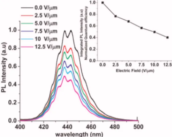
The electric field dependent steady state PL measurement results are given in Fig. 2. The PL spectra exhibit a narrow-ing particularly with the longer wavelength part of the spec-tra shifting with the applied field due to partial compensation of polarization-induced built-in electric field inside the well layers. The normalized PL spectra depicted in Fig.3 clearly show this blueshift at the longer wavelengths, as a result of the reversed quantum confined Stark effect.8,13,14 This is an
FIG. 1. 共Color online兲 TRPL spectra of our polar InGaN/GaN quantum heterostructure under different electric field levels. The inset shows the car-rier lifetime vs. applied electric field as a result of the TRPL analysis.
FIG. 2. 共Color online兲 Steady-state PL spectra of our polar InGaN/GaN quantum heterostructure under different electric field levels. The integrated PL intensity for the corresponding electric field level is presented in the inset.
FIG. 3. 共Color online兲 Normalized PL spectra of our polar InGaN/GaN quantum heterostructure under electric field. We observe a narrowing of the spectra along with a blueshift in the longer wavelength region, with a zoom-in presented in the inset for clarity.
apparent sign that electric field dependence of transition en-ergy between the ground state electron and hole wave func-tions共具e1兩H兩h1典兲 is stronger than those between higher order states. From the definition of QE given in Eq.共1兲, we under-stand that the QE decreases with decreasing number of emit-ted photons 共Ne兲 in response to increasing external electric field, assuming that the application of electric field does not change the number of absorbed photons共Na兲. This condition is valid at such short excitation wavelengths in the ultraviolet for the low external electric field levels that we use in our characterization. The inset of Fig. 2shows the electric field dependence of PL intensity integrated over 440–470 nm cor-responding to 2.73⫾0.09 eV. This energy range we consid-ered in this partial integration spans the transition energy of ground state electron and hole for all electric field values. This shows the relative QE behavior as a function of applied field.
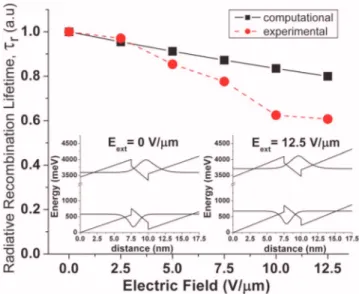
From the relative QE and carrier lifetime measurements, we can deduce relative radiative recombination lifetimes. As shown in Fig.4,rtends to decrease with increasing external electric field. The decrease of radiative recombination life-time is explained with the overlap integral of electron and hole ground states共calculated using transfer matrix method兲 that increases with increasing external electric field as given
for two of our cases in the inset of Fig.4. This is a result of the reversed quantum confined Stark effect and Fermi’s golden rule. Also in Fig. 4, we compare the normalized re-ciprocal of squared overlap integral of calculated electron and hole ground state wave functions with our experimental relative r results, both of which show the same trend of change in response to the applied field.
In conclusion, we presented radiative decay kinetics of polar InGaN/GaN quantum heterostructures and its electric field dependence at low applied fields. Our experimental measurements and numerical analyses show that the carrier lifetimes and radiative recombination lifetimes both decrease with increasing external electric field. However, the radiative component demonstrates comparatively a weaker depen-dence on the electric field, while the overall PL kinetics ex-hibits a stronger electric field dependence. As a result of our study, we qualitatively demonstrate and verify a fundamental physics concept, Fermi’s golden rule, to be dependent on external electric field in a polar InGaN/GaN quantum hetero-structure.
1S. Nakamura, M. Senoh, N. Iwasa, and S. Nagahama,Appl. Phys. Lett.
67, 1868共1995兲.
2C. Huh, H.-S. Kim, S.-W. Kim, J.-M. Lee, D.-J. Kim, I.-H. Lee, and S.-J.
Park,J. Appl. Phys. 87, 4464共2000兲.
3E. F. Schubert and J. K. Kim,Science 308, 1274共2005兲.
4S. Nakamura, M. Senoh, S. Nagahama, N. Iwasa, T. Yamada, T.
Mat-sushita, Y. Sugimoto, and H. Kiyoku,Appl. Phys. Lett. 69, 4056共1996兲.
5M. Hansen, P. Fini, L. Zhao, A. C. Abare, L. A. Coldren, and J. S. Speck, Appl. Phys. Lett. 76, 529共2000兲.
6S. Nakamura, S. J. Pearton, and G. Fasol, The Blue Laser Diode共Springer,
Berlin, 1997兲.
7M. Kneissl, T. L. Paoli, P. Kiesel, D. W. Treat, M. Teepe, N. Miyashita,
and N. M. Johnson,Appl. Phys. Lett. 80, 3283共2002兲.
8E. Sari, T. Ozel, S. Nizamoglu, and H. V. Demir,Appl. Phys. Lett. 90,
011101共2007兲.
9T. Ozel, E. Sari, S. Nizamoglu, and H. V. Demir, J. Appl. Phys. 102,
113101共2007兲.
10V. Fiorentini, F. Bernardini, F. D. Sala, A. Di Carlo, and P. Lugli,Phys. Rev. B 60, 8849共1999兲.
11T. Takeuchi, C. Wetzel, S. Yamaguchi, H. Sakai, H. Amano, I. Akasaki, Y.
Kaneko, S. Nakagawa, Y. Yamaoka, and N. Yamada,Appl. Phys. Lett. 73, 1691共1998兲.
12Y. D. Jho, J. S. Yahng, E. Oh, and D. S. Kim,Phys. Rev. B 66, 035334
共2002兲.
13D. A. B. Miller, D. S. Chemla, T. C. Damen, A. C. Gossard, W.
Wieg-mann, T. H. Wood, and C. A. Burrus,Phys. Rev. B 32, 1043共1985兲.
14L. I. Gurinovich, M. V. Artemyev, U. Woggon, Physics, Chemistry and
Applications of Nanostructures 共Reviews and Short Notes to
Nanomeeting-2001兲, 2001 共unpublished兲, pp. 150–155. FIG. 4. 共Color online兲 Relative radiative recombination lifetime extracted
from TRPL and PL measurements. The inset shows energy band diagrams corresponding electron and hole ground state wave functions for the case of 0 V/m and 12.5 V/m externally applied electric field.