Low dark current metal-semiconductor-metal photodiodes based on semi-insulating
GaN
Serkan Butun, Mutlu Gökkavas, HongBo Yu, and Ekmel Ozbay
Citation: Appl. Phys. Lett. 89, 073503 (2006); doi: 10.1063/1.2234741 View online: http://dx.doi.org/10.1063/1.2234741
View Table of Contents: http://aip.scitation.org/toc/apl/89/7
Published by the American Institute of Physics
Articles you may be interested in
Assessment of GaN metal–semiconductor–metal photodiodes for high-energy ultraviolet photodetection
Applied Physics Letters 80, 3198 (2002); 10.1063/1.1475362
Gain mechanism in GaN Schottky ultraviolet detectors
Applied Physics Letters 79, 1417 (2001); 10.1063/1.1394717
Visible-blind GaN Schottky barrier detectors grown on Si(111)
Applied Physics Letters 72, 551 (1998); 10.1063/1.120755
Comprehensive characterization of metal–semiconductor–metal ultraviolet photodetectors fabricated on single-crystal GaN
Journal of Applied Physics 83, 6148 (1998); 10.1063/1.367484
Growth of high crystalline quality semi-insulating GaN layers for high electron mobility transistor applications
Journal of Applied Physics 100, 033501 (2006); 10.1063/1.2221520
Ultrafast metal-semiconductor-metal photodetectors on low-temperature-grown GaN
Low dark current metal-semiconductor-metal photodiodes based
on semi-insulating GaN
Serkan Butuna兲
Nanotechnology Research Center, Bilkent University, Bilkent, Ankara 06800, Turkey and Department of Physics, Bilkent University, Bilkent, Ankara 06800, Turkey
Mutlu Gökkavas and HongBo Yu
Nanotechnology Research Center, Bilkent University, Bilkent, Ankara 06800, Turkey
Ekmel Ozbay
Nanotechnology Research Center, Bilkent University, Bilkent, Ankara 06800, Turkey;
Department of Physics, Bilkent University, Bilkent, Ankara 06800, Turkey; and Department of Electrical and Electronics Engineering, Bilkent University, Bilkent, Ankara 06800, Turkey
共Received 5 April 2006; accepted 2 June 2006; published online 15 August 2006兲
Metal-semiconductor-metal photodetectors on semi-insulating GaN templates were demonstrated and compared with photodetectors fabricated on regular GaN templates. Samples were grown on a metal organic chemical vapor deposition system. Devices on semi-insulating template exhibited a dark current density of 1.96⫻10−10A / cm2at 50 V bias, which is four orders of magnitude lower compared with devices on regular template. Device responsivities were 101.80 and 88.63 A / W at 50 V bias for 360 nm ultraviolet illumination for semi-insulating and regular templates, respectively. Incident power as low as 3 pW was detectable using the devices that were fabricated on the semi-insulating template. © 2006 American Institute of Physics.关DOI:10.1063/1.2234741兴
Solid state photodetectors based on AlxGa1−xN based 共0艋x艋1兲 heterostructures are promising candidates for photodetection in the ultraviolet 共UV兲 spectrum from the near UV to deep UV. A variety of UV photodetectors, such as Schottky barrier,1,2 p-i-n,3–5 and metal-semiconductor-metal6–8 共MSM兲 photodetectors, based on this material system have been reported in the literature. Al-though structures with high Al content exhibited low dark current values, there have only been a few reports regarding relatively low dark current devices fabricated on GaN. The best result was around 10 pA at 100 V bias.9 In this letter, we report the fabrication and characterization of MSM pho-todetectors that are based on semi-insulating共SI兲 GaN. Iden-tical devices fabricated on regular unintentionally doped 共UD兲 GaN epilayers were used to make a comparison and evaluate the improvement by using the SI-GaN template.
The samples in this study were all grown on c-face 共0001兲 sapphire substrates by low-pressure metal organic chemical vapor deposition 共MOCVD兲. Hydrogen was used as the carrier gas, and trimethylgallium共TMGa兲, trimethyla-luminum共TMAl兲, and ammonia 共NH3兲 were used as the Ga, Al, and N sources, respectively. SI-GaN layer was grown on high temperature AlN buffer. Prior to the epitaxial growth, sapphire substrates were annealed at 1100 ° C for 10 min to remove surface contamination, and subsequently a 15 nm thick AlN nucleation layer was deposited at 840 ° C. There-after, the reactor temperature was ramped to 1150 ° C and an AlN buffer layer was grown, followed by a 2 min growth interruption in order to reach optimum growth conditions for GaN. The growth conditions of GaN were as follows: reactor pressure of 200 mbars, growth temperature of 1070 ° C, H2 carrier gas, and growth rate about 2m / h. A typical UD-GaN control sample was grown on sapphire substrate
using the two-step method with a low temperature GaN nucleation layer deposited at 500 ° C. For a fair comparison, the thickness and growth parameters of the high temperature GaN 共HT-GaN兲 layers in the two samples were kept constant.
We used a four-step microwave compatible process in a class-100 clean room environment to fabricate the MSM photodiodes. We started with the deposition of 100 Å / 1000 Å thick interdigitated Ni/ Au fingers on the sur-face of the UD-GaN and SI-GaN layers of the two samples. Finger width and spacing of fabricated devices varied be-tween 3 and 20m, while active detector areas were 100 ⫻100 and 200⫻200m2. Following finger deposition, the device mesas were defined by reactive ion etching. Next, a 120 nm thick Si3N4 layer was deposited by a plasma en-hanced chemical vapor deposition共PECVD兲 system for the surface passivation of the samples. The Si3N4layer was also used as an antireflection layer as well as for protecting the metal fingers. Finally, fabrication was finalized by the depo-sition of 10 nm/ 400 nm thick Ti/ Au interconnect pads. In addition, the transmission line method共TLM兲 patterns were prepared by the deposition of 100 Å / 400 Å / 100 Å / 400 Å Ti/ Al/ Ni/ Au contact pads on separate samples. The TLM patterns used for sheet resistivity calculations consisted of 200⫻100m2pads with separations in the 5 – 50m range. The contacts were annealed at 750 ° C for 1 min in a rapid thermal processor oven.
We calculated the sheet resistivities of the two samples using standard TLM measurements. Current-voltage 共I-V兲 characterization of the contact pads was carried out with an HP4142B semiconductor parameter analyzer. The sheet re-sistances of the SI-GaN and UD-GaN samples were calcu-lated as 3.16⫻1011and 5.8⫻107⍀/sq, respectively.
Current-voltage characterization of the fabricated MSM photodiodes was carried out using a Keithley 6517A high resistance electrometer with low noise triaxialcables. The
de-a兲Electronic mail: [email protected]
APPLIED PHYSICS LETTERS 89, 073503共2006兲
vices fabricated on the SI-GaN sample exhibited extremely low dark currents, while those fabricated on the UD-GaN sample exhibited higher dark currents, which is typical for such devices. No breakdown was observed for bias voltages as high as 200 V for 200⫻200m2 active area detectors fabricated on the SI-GaN and UD-GaN samples. Figure 1 compares the dark I-V curves of 10m finger width/spacing devices from the two chips. The dark current measured from devices fabricated on the SI-GaN chip remains below 1 pA and up to 100 V bias voltage. The dark current density共at 50 V bias兲 of a device fabricated on the SI-GaN chip is cal-culated as 1.96⫻10−10A / cm2. In comparison, the 50 V dark current density calculated for a similar device fabricated on the UD-GaN chip is 8.1⫻10−6 A / cm2, which corresponds to four orders of magnitude improvement.
Spectral responsivity measurements of both samples were performed in the range of 250– 450 nm using a Xe arc lamp, a monochromator, and a calibrated Si photodetector which is calibrated through the range of 190– 1100 nm. Pho-tocurrent was measured in two different ways: The dc 共un-modulated兲 photocurrent was measured using a high resis-tance electrometer, whereas the ac共modulated兲 photocurrent was recorded by a lock-in amplifier using an optical chopper to modulate the monochromator output. Figure 2 illustrates unmodulated responsivity curves as a function of applied bias voltage for 200⫻200m2 devices with 3m / 3m finger width/spacing on the two different chips.
Devices on both chips exhibited a sharp cutoff at 365 nm, while the peak of the photoresponse was observed at 360 nm. Device responsivity increased with applied volt-age and reached 101.80 A / W for SI GaN and 88.63 A / W for UD GaN at 50 V bias and 365 nm UV illumination. These very high responsivity values indicate that devices have a gain of about 700 that can be attributed to the photo-conductive gain mechanism in MSM detectors. Using ther-mally limited detectivity 共D*兲 formula,10
D*= R
冑
R0A / 4kT, where Ris device responsivity at 0 V bias, R0is differential resistance, and A is the device area, we find detectivity val-ues of 1.3⫻1014 and 1.2⫻1013cm Hz1/2/ W at 360 nm at 0 V bias for SI-GaN and UD-GaN chips, respectively. Detectivity of the SI-GaN sample reached 3.12 ⫻1017cm Hz1/2/ W at 50 V bias. These detectivity values are the best results reported in the literature for a GaN based MSM photodiode. These high detectivity values are even comparable with those of photomultiplier tubes and AlGaNbased photodetectors.11,12 We also performed a modulated photoresponse measurement in order to investigate the de-pendence of the gain on modulation frequency. Figure 3 shows the photoresponse of a device on the SI-GaN sample. Although device responsivity decreases with the chopper fre-quency as expected,13 a significant gain is observed even at the setup high frequency limit of 400 Hz.
Finally, a low optical power responsivity measurement was performed in order to determine the minimum detectable
FIG. 1. Current-voltage characteristics of 200⫻200m2 MSM
photo-diodes with 10m / 10m finger width/spacing on two different chips.
FIG. 2. Measured spectral responsivity curves of 200⫻200m2devices
with 3m / 3m finger width/spacing on the 共a兲 UD-GaN chip and 共b兲 SI-GaN chip as a function of applied bias voltage.
FIG. 3. Normalized modulated photoresponse of a 200⫻200m2device
with 3m / 3m finger width/spacing on the SI-GaN chip as a function of chopper frequency.
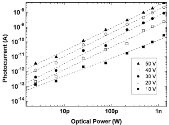
optical power. A series of neutral density filters were used to vary the incident optical power in the range of a few picow-atts to 1 nW. As expected, very low level signals are detect-able because of the large gain and low dark current values. As shown in Fig. 4, the measured dc photocurrent is well above the dark current at the corresponding bias voltage even for incident optical powers as low as 3 pW.
In conclusion, we have fabricated and tested MSM pho-todiodes on SI-GaN templates. We also compared these de-vices with identical ones fabricated on a regular UD-GaN control sample. Devices on the SI-GaN chip exhibited a dark current density of 1.96⫻10−10A / cm2 at 50 V bias voltage, which is four orders of magnitude lower compared with that of the devices on the UD-GaN chip. No sign of device break-down was observed at bias voltages as high as 200 V for both samples. For 360 nm UV illumination and at 50 V bias, responsivity values as high as 101.8 and 88.63 A / W were obtained from the SI- and UD-GaN samples, respectively.
Photoresponse of both samples was comparable with no sig-nificant difference. All of the devices exhibited relatively flat response in the 250– 360 nm range with a sharp cutoff at 365 nm. Because of high internal gain and low dark current, MSM photodetectors fabricated on SI-GaN templates can de-tect low level optical signals on the order of a few picowatts. This work was supported by EU NOE-PHOREMOST, EU NOE-METAMORPHOSE, and TUBITAK under Project Nos. 104E090, 105E066, and 105A005. One of the authors 共E.O.兲 acknowledges partial support from the Turkish Acad-emy of Sciences.
1A. Osinsky, S. Gangopadhyay, B. W. Lim, M. Z. Anwar, M. A. Khan, D.
V. Kuksenkov, and H. Temkin, Appl. Phys. Lett. 72, 742共1998兲.
2T. Tut, N. Biyikli, I. Kimukin, T. Kartaloglu, O. Aytur, M. S. Unlu, and E.
Ozbay, Solid-State Electron. 49, 117共2005兲.
3U. Chowdhury, M. M. Wong, C. J. Collins, B. Yang, J. C. Denyszyn, J. C.
Campbell, and D. Dupuis, J. Cryst. Growth 248, 552共2003兲.
4C. J. Collins, U. Chowdhury, M. M. Wong, B. Yang, A. L. Beck, R. D.
Dupuis, and J. C. Campbell, Appl. Phys. Lett. 80, 3754共2002兲.
5M. M. Wong, U. Chowdhury, C. J. Collins, B. Yang, J. C. Denyszyn, K. S.
Kim, J. C. Campbell, and R. D. Dupuis, Phys. Status Solidi A 188, 333 共2001兲.
6T. Li, D. J. H. Lambert, A. L. Beck, C. J. Collins, B. Yang, J. M. M. Wong,
U. Chowdhury, R. D. Dupuis, and J. C. Campbell, Electron. Lett. 36, 1581共2000兲.
7N. Biyikli, I. Kimukin, T. Kartaloglu, O. Aytur, and E. Ozbay, Phys. Status
Solidi C 7, 2314共2003兲.
8J. Y. Duboz, J. L. Reverchon, D. Adam, B. Damilano, N. Grandjean, F.
Semond, and J. Massies, J. Appl. Phys. 92, 5602共2002兲.
9E. Monroy, T. Palacios, O. Hainaut, F. Omnes, F. Calle, and J. F.
Hochedez, Appl. Phys. Lett. 80, 3198共2002兲.
10S. Donati, Photodetectors: Devices, Circuits, and Applications
共Prentice-Hall, Upper Saddle River, NJ, 2000兲, p. 43.
11J. D. Brown, Z. Yu, J. Matthews, S. Harney, J. Boney, J. F. Schetzina, J. D.
Jenson, K. W. Dang, C. Terrill, T. Nohava, W. Yang, and S. Krishnankutty, MRS Internet J. Nitride Semicond. Res. 4, 9共1999兲.
12N. Biyikli, I. Kimukin, O. Aytur, and E. Ozbay, IEEE Photonics Technol.
Lett. 16, 1718共2004兲.
13P. Kung, X. Zhang, D. Walker, A. Saxler, J. Piotrowski, A. Rogalski, and
M. Razeghi, Appl. Phys. Lett. 67, 3792共1995兲. FIG. 4. Measured photocurrent of a 200⫻200m2 device with
3m / 3m finger width/spacing on the SI-GaN chip as a function of op-tical power and bias voltage. The dashed lines represent linear fits to the plotted data.