364 IEEE PHOTONICS TECHNOLOGY LETTERS, VOL. 18, NO. 2, JANUARY 15, 2006
Low-Power Thermooptical Tuning of SOI
Resonator Switch
Isa Kiyat, Student Member, IEEE, Atilla Aydinli, Member, IEEE, and Nadir Dagli, Senior Member, IEEE
Abstract—A wavelength selective optical switch is developed based on a high- racetrack resonator making use of the large thermooptic coefficient of silicon. The racetrack resonator was fabricated using a silicon-on-insulator (SOI) single-mode rib waveguide. The resonator shows a high factor of 38 000 with spectral sidelobes of 11 dB down and can be thermooptically scanned over its full free-spectral range applying only 57 mW of electrical power. A low power of 17 mW is enough to tune the de-vice from resonance to off-resonance state. The dede-vice functions as a wavelength selective optical switch with a 3-dB cutoff frequency of 210 kHz.
Index Terms—Integrated optics, resonator, thermooptical switch, thermooptical tuning, silicon-on-insulator (SOI) tech-nology.
I. INTRODUCTION
R
ESEARCH activities in silicon-based integrated optics have increased dramatically during the past ten years [1]. These activities in the field can be related to the development of high-quality silicon-on-insulator (SOI) wafers at low cost [1]. SOI technology opens the possibility for integration of photonic and microelectronic devices on the same wafer. Therefore, it is not surprising that a lot of the effort spent in the field of integrated optics is devoted to realization of devices on an SOI platform. So far, many integrated optical devices including light couplers, splitters, modulators, and ring resonators have been proposed and fabricated using the SOI material system [1]–[4]. Among them, ring resonators are distinguished with their high wavelength selectivity, a key issue for many device applications ranging from wavelength multiplexers [5] to mod-ulators [6]. Recently, high- resonator-based modulators with significantly lower switching powers have become an important alternative to Mach–Zehnder (MZ) modulators. The ability to tune the output wavelength is the first step to the development of devices for applications such as optical modulators and switches. The wavelength tuning capability is also required to fine tune to the desired wavelength when the target wavelength is not met during the fabrication process, due to imperfections or material nonuniformity. Electrooptical [6], thermooptical [7], and all-optical [8] tuning are the most commonly used mechanisms in device applications. The electrooptical effect can be implemented for fast tuning and switching on compoundManuscript received July 18, 2005; revised November 4, 2005. This work was supported by Bilkent University under Grant Phys03-02.
I. Kiyat and A. Aydinli are with Turk Telekom Bilkent Laboratories, Depart-ment of Physics, Bilkent University, Ankara 06800, Turkey.
N. Dagli is with the Electrical and Computer Engineering Department, Uni-versity of California, Santa Barbara, CA 93106 USA.
Digital Object Identifier 10.1109/LPT.2005.861951
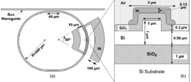
Fig. 1. Schematic views showing critical dimensions. (a) Top view of SOI resonator and (b) cross-sectional view of SOI rib waveguide.
semiconductors. However, silicon lacks inversion symmetry and an electrooptic coefficient and, therefore, does not lend itself to this mechanism. On the other hand, silicon is known for its large thermooptic coefficient [9]. Use of the thermoop-tical effect in silicon devices is a simple, straightforward, and cost-effective way for applications requiring tuning and moderate modulation speeds.
SOI rib waveguides having dimensions of the order of 1 m have become a new branch of optical SOI waveguides [10]. These waveguides have sizes smaller than the conventional large cross-section SOI waveguides (3 m) but larger than those of SOI nanowires (0.4 m). Their geometrically controllable bire-fringence has been used to realize polarization splitters [3] and polarization-independent racetrack resonators [11] on SOI. Fur-thermore, for a waveguide width of 1 m, bending losses can be kept quite low for radii as small as 150 m, thereby allowing the fabrication of high- resonators with this dimension [12].
In this letter, we demonstrate thermooptical tuning of a high- racetrack resonator on an SOI rib waveguide of 1- m size and its operation as a low-power optical switch. Electrical powers as low as 57 and 17 mW are sufficient to scan over the full free-spectral range and use the resonator as an optical switch, respectively.
II. FABRICATION ANDEXPERIMENT
Fig. 1(a) shows a schematic top view of the designed SOI resonator with the metal heater and contact pads. The cross-sec-tional detail of the SOI waveguide is also shown in Fig. 1(b). This SOI waveguide geometry optimized by beam propagation (BPM) method simulations has been experimentally proved to be single mode. These low-loss single-mode rib waveguides have already been used in the demonstration of polarization splitters and high- racetrack resonators [3], [12]. All pattern definitions throughout the fabrication of SOI resonators and their thermooptical tuning elements were done with optical
KIYAT et al.: LOW-POWER THERMOOPTICAL TUNING OF SOI RESONATOR SWITCH 365
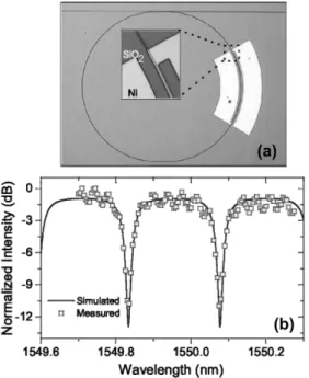
Fig. 2. (a) Optical micrographs showing top view of fabricated racetrack resonator and overlaying metal heater. (b) Measured and simulated TE transmission spectrum of fabricated SOI rib waveguide racetrack resonator.
contact photolithography. Resonator patterns were defined on an SOI wafer which had a 1.00- m top Si and a 1.00- m oxide layer on a 625- m-thick substrate. The patterns were trans-ferred to a silicon layer of 0.42 m using a reactive ion-etching (RIE) process resulting in smooth sidewalls [12]. The etch was followed by deposition of about 0.3 m SiO passivation layer using plasma-enhanced chemical vapor deposition at 250 C. The 0.12- m-thick nickel heaters and contact pads were then defined through a process sequence comprising pho-tolithography, metal sputtering, and liftoff steps. The optical micrographs of a finished resonator and its overlaying metal heater are shown in Fig. 2(a).
We cleaved the wafer to a chip of 8-mm length. Light from a high-resolution ( 1 pm) external cavity tunable laser was end-fire coupled to the bus waveguide with a tapered and lensed fiber producing a 2- m spot. The light passing through the de-vice was collected with a microscope objective and focused on a Ge detector. The measured transmission spectrum of the resonator with radius of 400 m, straight coupling section of 48 m, and coupling gap of 0.8 m is given in Fig. 2(b) for TE polarization. The simulated spectrum of the resonator using the well-known power transmission expression of a single-ring res-onator [12, eq. 1] is also plotted in the figure. We used BPM cal-culated coupling factors as initial values in the simulation. After a few iterations, a coupling factor of 0.45 and resonator round trip loss of 1.57 dB was obtained. This is to be expected since we have already shown in [12] that SOI rib bend waveguides used in this letter with a radius of 300 m or larger do not suffer from radiation loss due to curvature. Scattering from imperfections due to fabrication and material nonuniformity are estimated to be the main sources of resonator loss. The fiber-to-fiber inser-tion loss was measured to be 19 dB with unpolished waveguide facets which were not antireflective (AR) coated. The free-spec-tral range can be determined to be 248 pm from the figure.
Fig. 3. (a) Measured TE transmission spectrum as electrical power applied to metal heater. (b) Shift in resonance wavelength as function of applied power.
The resonator shows good modulation characteristics with spec-tral side lobes of 11 dB down. The full-width at half-maximum (bandwidth) was extracted from the data using a curve fitting of 40 pm. Using this value with resonance wavelength and the free-spectral range of the resonator, we calculated a -factor of 38 000 and a finesse value of 6.2.
The resonance wavelengths of a resonator are deter-mined through the roundtrip phase term
and can be tuned by either changing the resonator circum-ference or the effective index . Silicon is known for its large thermooptical coefficient of 1.84 10 C , which has been employed to realize modulators on SOI wafers [9]. Ther-mooptical modulation of an effective refractive index is attained by placing a metal heater electrode near the waveguide. High-resonators have narrow bandwidths and can be tuned to off-res-onance with lower electrical powers [7]. After passive charac-terization of the resonator, we applied electrical power to the contact pads using microprobes. The heater is a 0.12- m-thick and 3- m-wide nickel layer in the shape of a circular bend to assure maximum overlapping of heat flow with the optical field in the resonator. It is just above the rib of the waveguide with only a 0.3- m-thick layer of SiO in between (Fig. 1). The bend-shaped heater spans an angle of 60 . The 100- m-wide nickel contact pads were also designed in a circular shape. They are well separated from the heater [Figs. 1(a) and 2(a)]. The pads and heater combination was measured to have a resistance of 170 . The measured transmission spectra of the resonator under applied power are shown for four different applied power values in Fig. 3(a). The transmission spectrum does not change with applied power (except for experimental error), since nei-ther the propagation loss nor the coupling depends on the ap-plied power within the limits used in the experiment. There is a smooth tuning of resonance wavelength with applied power. We also plot the resonance wavelength shift as a function of applied electrical power in Fig. 3(b). It can be deduced from the figure
366 IEEE PHOTONICS TECHNOLOGY LETTERS, VOL. 18, NO. 2, JANUARY 15, 2006
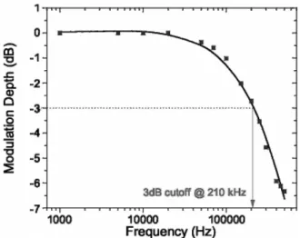
Fig. 4. Measured small signal modulation response.
that a total of 57 mW of electrical power is sufficient to scan the resonator over its full free-spectral range.
An equation-relating change in the effective index to the mea-sured change in resonance wavelength can be derived from the resonance condition as
(1) where is the shift in resonance wavelength . The geo-metrical term is due to the fact that the heater does not have the same length as the circumference of the resonator. From Fig. 3(b), we find that, 17 mW of electrical power re-sulting in a shift of 57 pm in the spectrum is sufficient to switch the resonator from theOFF(at resonance wavelength) toON(at off-resonance wavelengths) state. Substituting in (1), is calculated for switching from the
OFFtoON state at a given wavelength. We can express
as . is a waveguide
geom-etry-dependent term; however, we can calculate the minimum change in local temperature to be 4.19 C by approximating
.
To observe the frequency response of the switch, applied power was modulated by a small signal sinusoidal driving voltage. The optical signal was monitored with an InGaAs photodetector of 70-MHz bandwidth. Normalized modulation depth versus driving voltage frequency for the switch is plotted in Fig. 4. A relatively high 3-dB cutoff frequency of 210 kHz was found for the device. This limit is due to extrinsic thermal effects since the intrinsic bandwidth limitation due to the build up and decay of the resonance is estimated to be of the order of several tens of gigahertz. To the best of our knowledge, this device is the fastest thermooptic SOI ring resonator switch, to date, with no differential control. The polarization dependence of such devices is studied in [13].
III. CONCLUSION
In summary, an SOI optical rib waveguide resonator is fab-ricated through a single-etch step and characterized to show a high factor of 38 000. This resonator shows thermooptical tunability and operates as a wavelength-selective optical switch with low-power consumption of 17 mW. The device was tested to function as a switch at frequencies up to 210 kHz.
ACKNOWLEDGMENT
The authors would like to thank Dr. A. Dane and A. Kocabas for their help with the frequency response measurements and useful discussions.
REFERENCES
[1] B. Jalali, S. Yagnanarayanan, T. Yoon, T. Yoshimoto, I. Rendina, and F. Coppinger, “Advances in silicon-on-insulator optoelectronics,” IEEE J.
Sel. Topics Quantum Electron., vol. 4, no. 6, pp. 938–947, Dec. 1998.
[2] P. D. Trinh, S. Yagnanarayanan, and B. Jalali, “Integrated optical direc-tional couplers in silicon-on-insulator,” Electron. Lett., vol. 31, no. 24, pp. 2097–2098, 1995.
[3] I. Kiyat, A. Aydinli, and N. Dagli, “A compact silicon-on-insulator polarization splitter,” IEEE Photon. Technol. Lett., vol. 17, no. 1, pp. 100–102, Jan. 2005.
[4] B. E. Little, J. S. Foresi, G. Steinmeyer, E. R. Thoen, S. T. Chu, H. Haus, E. P. Ippen, L. C. Kimerling, and W. Greene, “Ultra-compact Si–SiO microring resonator optical channel dropping filters,” IEEE
Photon. Technol. Lett., vol. 10, no. 4, pp. 549–551, Apr. 1998.
[5] E. Little, S. T. Chu, P. P. Absil, J. V. Hryniewicz, F. G. Johnson, F. Seifert, D. Gill, V. Van, O. King, and M. Trakalo, “Very high-order microring resonator filters for WDM applications,” IEEE Photon. Technol. Lett., vol. 16, no. 10, pp. 2263–2265, Oct. 2004.
[6] T. Sadagopan, S. June Choi, K. Djordjev, and P. D. Dapkus, “Carrier-induced refractive index changes in InP-based circular microresonators for low-voltage high-speed modulation,” IEEE Photon. Technol. Lett., vol. 17, no. 2, pp. 414–416, Feb. 2005.
[7] W. M. J. Green, R. K. Lee, G. A. DeRose, A. Scherer, and A. Yariv, “Hybrid InGaAsP-InP Mach–Zehnder racetrack rasonator resonator for thermooptic switching and coupling control,” Opt. Expr., vol. 13, no. 5, pp. 1651–1659, 2005.
[8] V. R. Almeida, C. A. Barrios, R. R. Panepucci, M. Lipson, M. A. Foster, D. G. Ouzounov, and A. L. Geata, “All-optical switching on a silicon chip,” Opt. Lett., vol. 29, no. 24, pp. 2867–2869, 2004.
[9] R. L. Espinola, M. C. Tsai, J. T. Yardley, and R. M. Osgood Jr., “Fast and low-power thermooptic switch on thin silicon-on-insulator,” IEEE
Photon. Technol. Lett., vol. 15, no. 10, pp. 1366–1368, Oct. 2003.
[10] W. S. P. Chan, C. E. Png, S. T. Lim, G. T. Reed, and V. M. N. Passaro, “Single-mode and polarization-independent silicon-on-insulator waveg-uides with small cross section,” J. Lightw. Technol., vol. 23, no. 6, pp. 2103–2111, Jun. 2005.
[11] W. R. Headley, G. T. Reed, S. Howe, A. Liu, and M. Paniccia, “Polariza-tion-independent optical racetrack resonators using rib waveguides on silicon-on-insulator,” Appl. Phys. Lett., vol. 85, no. 23, pp. 5523–5525, 2004.
[12] I. Kiyat, A. Aydinli, and N. Dagli, “High-Q silicon-on-insulator op-tical rib waveguide racetrack resonators,” Opt. Expr., vol. 13, no. 6, pp. 1900–1905, 2005.
[13] , “Compact large cross section silicon-on-insulator racetrack res-onators,” IEEE Photon. Technol. Lett., vol. 17, no. 10, pp. 2098–2100, Oct. 2005.