Laser-micromachined millimeter-wave photonic band-gap cavity structures
E. Özbay, G. Tuttle, J. S. McCalmont, M. Sigalas, R. Biswas, C. M. Soukoulis, and K. M. Ho
Citation: Appl. Phys. Lett. 67, 1969 (1995); doi: 10.1063/1.114756 View online: http://dx.doi.org/10.1063/1.114756
View Table of Contents: http://aip.scitation.org/toc/apl/67/14
Laser-micromachined millimeter-wave photonic band-gap cavity structures
E. O¨ zbaya)
Department of Physics, Bilkent University, Bilkent, Ankara 06533, Turkey
G. Tuttle, J. S. McCalmont, M. Sigalas, R. Biswas, C. M. Soukoulis, and K. M. Ho Microelectronics Research Center and DOE Ames Laboratory, Iowa State University, Ames, Iowa 50011 ~Received 12 June 1995; accepted for publication 26 July 1995!
We have used laser-micromachined alumina substrates to build a three-dimensional photonic band-gap crystal. The rod-based structure has a three-dimensional full photonic band gap between 90 and 100 GHz. The high resistivity of alumina results in a typical attenuation rate of 15 dB per unit cell within the band gap. By removing material, we have built defects which can be used as millimeter-wave cavity structures. The resulting quality~Q! factors of the millimeter-wave cavity structures were as high as 1000 with a peak transmission of 10 dB below the incident signal. © 1995 American Institute of Physics.
Propagation of electromagnetic~EM! waves in periodic dielectric structures can be completely forbidden for a certain range of frequencies.1,2 These three-dimensional arrays— photonic band-gap~PBG! crystals—can be used to engineer the properties of the radiation field within these structures.3,4 For example, PBG crystals can be used to inhibit spontane-ous emission in photonic devices, leading to more efficient light emitters like thresholdless semiconductor lasers and single-mode light-emitting diodes.5–7 However, the difficul-ties of fabricating structures at dimensions close to optical wavelengths restricted the experimental demonstration of the early PBG crystals to microwave frequencies~12–15 GHz!. Recently, we designed a three-dimensional layer-by-layer structure which alleviates some of the fabrication difficulties inherent with the earlier designs.8Using a large scale model made of cylindrical alumina rods, we confirmed the exist-ence of a full photonic band gap at microwave frequencies
~12–14 GHz!.9 Using micromachined silicon wafers, we
subsequently fabricated smaller scale structures with photo-nic band-gap frequencies ranging from 100 to 500 GHz.10–12 The frequency range of these photonic crystals are suitable for a number of millimeter and submillimeter wave applica-tions, including efficient millimeter wave antennas, filters, sources, and waveguides.13–16However, most of these appli-cations are based on the presence of defect or cavity modes which are obtained by locally disturbing the periodicity of the photonic crystal.17–19The frequencies of these modes lie within the forbidden band gap of the pure crystal, and the associated fields are localized around the defect. We have recently demonstrated that defect structures can be built around our layer-by-layer structure at microwave frequencies
~13 GHz!.20 In this letter, we demonstrate the existence of
such cavity structures at millimeter-wave frequencies by us-ing a laser-micromachined PBG crystal.
In our initial investigations of defects in millimeter-wave structures, we looked at defects incorporated into our earlier silicon micromachined structures.17Although silicon micro-machining has proven to be very successful for building three-dimensional photonic crystals, we found that defects
incorporated into our structures had relatively poor qualities. In particular, peak transmission of the defect mode was low
~220 dB below the incident signal! and the Q-factor ~quality
factor, defined as the center frequency divided by the peak’s full width at half-maximum! of the resonance was also low
~;100!. We attribute these effects to the relatively low
resis-tivity of our silicon wafers~30–180 V cm!. Our calculations show that the transmission at the top of the defect peak and the Q-factor decrease drastically as one increases the conduc-tivity of the Si wafers. As an alternative to using even higher resistivity silicon, we have investigated the use of alumina as the dielectric material for defect structures. Alumina with a typical resistivity six orders of magnitude larger than the resistivity of silicon would be a good dielectric material to build high-Q cavity structures. In order to build alumina based millimeter wave photonic crystals, we have patterned the wafers by means of laser machining.
The square-shaped alumina wafers ~Kyocera 96% alu-mina: resistivity .10101/2-cm, refractive index52.86 at 100 GHz! used in this work were each 5.1 cm35.1 cm, and 400
mm thick. The pattern consists of 24 parallel stripes, each 460 mm wide and separated by 840 mm wide gaps for a filling ratio of 0.36. These stripe dimensions and the wafer thickness determine the center of the forbidden photonic gap—calculated to be 94.7 GHz in this case. The stripes are 3.1 cm long so that the 24 stripes form a square 3.1 cm33.1 cm pattern. The stripes are cut using a high power carbon dioxide laser.21
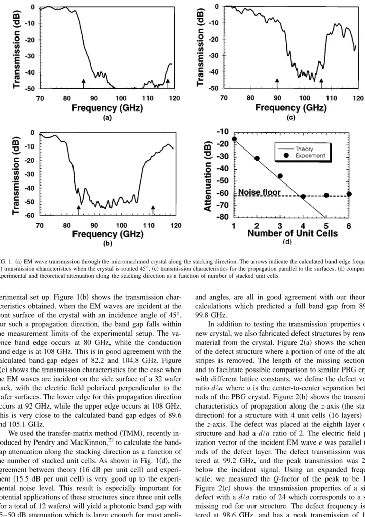
The laser-machined wafers are stacked to form the pho-tonic crystal, using a holder with pins that aligned the guide holes that were machined through the alumina wafers. This stacking process which was previously used to build silicon micromachined photonic crystals,6 results in a stacking se-quence that repeats every four layers, corresponding to a single unit cell along the stacking direction. Using a W-band network analyzer, the transmission characteristics of the crystal are measured. Figure 1~a! shows the EM wave trans-mission through the laser-machined crystal in which the wave vector of the incident EM wave is normal to the wafer surfaces. For propagation along the stacking direction, the lower edge of the photonic gap occurs at 85 GHz, while the conduction band is beyond the measurement limit of the
ex-a!Electronic mail: [email protected]
1969 Appl. Phys. Lett. 67 (14), 2 October 1995 0003-6951/95/67(14)/1969/3/$6.00 © 1995 American Institute of Physics
perimental set up. Figure 1~b! shows the transmission char-acteristics obtained, when the EM waves are incident at the front surface of the crystal with an incidence angle of 45°. For such a propagation direction, the band gap falls within the measurement limits of the experimental setup. The va-lence band edge occurs at 80 GHz, while the conduction band edge is at 108 GHz. This is in good agreement with the calculated band-gap edges of 82.2 and 104.8 GHz. Figure 1~c! shows the transmission characteristics for the case when the EM waves are incident on the side surface of a 32 wafer stack, with the electric field polarized perpendicular to the wafer surfaces. The lower edge for this propagation direction occurs at 92 GHz, while the upper edge occurs at 108 GHz. This is very close to the calculated band gap edges of 89.6 and 105.1 GHz.
We used the transfer-matrix method~TMM!, recently in-troduced by Pendry and MacKinnon,22to calculate the band-gap attenuation along the stacking direction as a function of the number of stacked unit cells. As shown in Fig. 1~d!, the agreement between theory ~16 dB per unit cell! and experi-ment ~15.5 dB per unit cell! is very good up to the experi-mental noise level. This result is especially important for potential applications of these structures since three unit cells
~for a total of 12 wafers! will yield a photonic band gap with
45–50 dB attenuation which is large enough for most appli-cations. The transmission characteristics of the structure along the aforementioned directions and for other directions
and angles, are all in good agreement with our theoretical calculations which predicted a full band gap from 89.6 to 99.8 GHz.
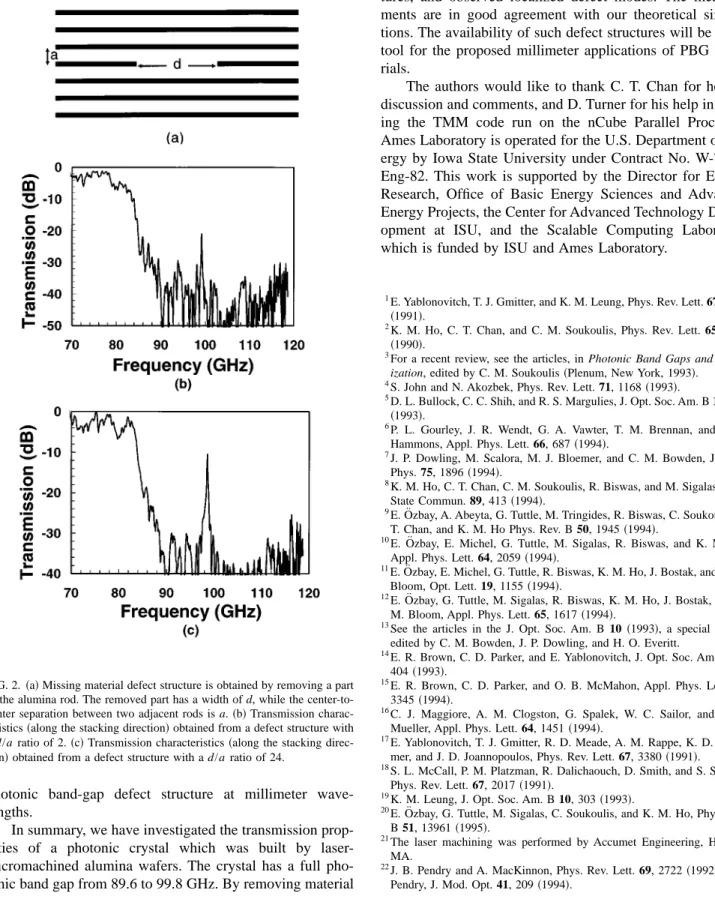
In addition to testing the transmission properties of the new crystal, we also fabricated defect structures by removing material from the crystal. Figure 2~a! shows the schematics of the defect structure where a portion of one of the alumina stripes is removed. The length of the missing section is d, and to facilitate possible comparison to similar PBG crystals with different lattice constants, we define the defect volume ratio d/a where a is the center-to-center separation between rods of the PBG crystal. Figure 2~b! shows the transmission characteristics of propagation along the z-axis ~the stacking direction! for a structure with 4 unit cells ~16 layers! along the z-axis. The defect was placed at the eighth layer of the structure and had a d/a ratio of 2. The electric field polar-ization vector of the incident EM wave e was parallel to the rods of the defect layer. The defect transmission was cen-tered at 99.2 GHz, and the peak transmission was 20 dB below the incident signal. Using an expanded frequency scale, we measured the Q-factor of the peak to be 1,030. Figure 2~c! shows the transmission properties of a similar defect with a d/a ratio of 24 which corresponds to a single missing rod for our structure. The defect frequency is cen-tered at 98.6 GHz, and has a peak transmission of 10 dB below the incident signal. To our knowledge these results correspond to the first demonstration of a three-dimensional
FIG. 1.~a! EM wave transmission through the micromachined crystal along the stacking direction. The arrows indicate the calculated band-edge frequencies, ~b! transmission characteristics when the crystal is rotated 45°, ~c! transmission characteristics for the propagation parallel to the surfaces, ~d! comparison of experimental and theoretical attenuation along the stacking direction as a function of number of stacked unit cells.
photonic band-gap defect structure at millimeter wave-lengths.
In summary, we have investigated the transmission prop-erties of a photonic crystal which was built by laser-micromachined alumina wafers. The crystal has a full pho-tonic band gap from 89.6 to 99.8 GHz. By removing material
from the crystals, we created millimeter wave defect struc-tures, and observed localized defect modes. The measure-ments are in good agreement with our theoretical simula-tions. The availability of such defect structures will be a key tool for the proposed millimeter applications of PBG mate-rials.
The authors would like to thank C. T. Chan for helpful discussion and comments, and D. Turner for his help in mak-ing the TMM code run on the nCube Parallel Processor. Ames Laboratory is operated for the U.S. Department of En-ergy by Iowa State University under Contract No. W-7405-Eng-82. This work is supported by the Director for Energy Research, Office of Basic Energy Sciences and Advanced Energy Projects, the Center for Advanced Technology Devel-opment at ISU, and the Scalable Computing Laboratory which is funded by ISU and Ames Laboratory.
1E. Yablonovitch, T. J. Gmitter, and K. M. Leung, Phys. Rev. Lett. 67, 2295
~1991!.
2K. M. Ho, C. T. Chan, and C. M. Soukoulis, Phys. Rev. Lett. 65, 3152
~1990!.
3For a recent review, see the articles, in Photonic Band Gaps and
Local-ization, edited by C. M. Soukoulis~Plenum, New York, 1993!.
4S. John and N. Akozbek, Phys. Rev. Lett. 71, 1168~1993!.
5D. L. Bullock, C. C. Shih, and R. S. Margulies, J. Opt. Soc. Am. B 10, 399
~1993!.
6P. L. Gourley, J. R. Wendt, G. A. Vawter, T. M. Brennan, and B. E.
Hammons, Appl. Phys. Lett. 66, 687~1994!.
7J. P. Dowling, M. Scalora, M. J. Bloemer, and C. M. Bowden, J. Appl.
Phys. 75, 1896~1994!.
8K. M. Ho, C. T. Chan, C. M. Soukoulis, R. Biswas, and M. Sigalas, Solid
State Commun. 89, 413~1994!.
9E. O¨ zbay, A. Abeyta, G. Tuttle, M. Tringides, R. Biswas, C. Soukoulis, C.
T. Chan, and K. M. Ho Phys. Rev. B 50, 1945~1994!.
10
E. O¨ zbay, E. Michel, G. Tuttle, M. Sigalas, R. Biswas, and K. M. Ho, Appl. Phys. Lett. 64, 2059~1994!.
11E. O¨ zbay, E. Michel, G. Tuttle, R. Biswas, K. M. Ho, J. Bostak, and D. M.
Bloom, Opt. Lett. 19, 1155~1994!.
12
E. O¨ zbay, G. Tuttle, M. Sigalas, R. Biswas, K. M. Ho, J. Bostak, and D. M. Bloom, Appl. Phys. Lett. 65, 1617~1994!.
13See the articles in the J. Opt. Soc. Am. B 10 ~1993!, a special feature
edited by C. M. Bowden, J. P. Dowling, and H. O. Everitt.
14E. R. Brown, C. D. Parker, and E. Yablonovitch, J. Opt. Soc. Am. B 10,
404~1993!.
15E. R. Brown, C. D. Parker, and O. B. McMahon, Appl. Phys. Lett. 64,
3345~1994!.
16C. J. Maggiore, A. M. Clogston, G. Spalek, W. C. Sailor, and F. M.
Mueller, Appl. Phys. Lett. 64, 1451~1994!.
17
E. Yablonovitch, T. J. Gmitter, R. D. Meade, A. M. Rappe, K. D. Brom-mer, and J. D. Joannopoulos, Phys. Rev. Lett. 67, 3380~1991!.
18S. L. McCall, P. M. Platzman, R. Dalichaouch, D. Smith, and S. Schultz,
Phys. Rev. Lett. 67, 2017~1991!.
19
K. M. Leung, J. Opt. Soc. Am. B 10, 303~1993!.
20E. O¨ zbay, G. Tuttle, M. Sigalas, C. Soukoulis, and K. M. Ho, Phys. Rev.
B 51, 13961~1995!.
21The laser machining was performed by Accumet Engineering, Hudson,
MA.
22
J. B. Pendry and A. MacKinnon, Phys. Rev. Lett. 69, 2722~1992!; J. B. Pendry, J. Mod. Opt. 41, 209~1994!.
FIG. 2.~a! Missing material defect structure is obtained by removing a part of the alumina rod. The removed part has a width of d, while the center-to-center separation between two adjacent rods is a.~b! Transmission charac-teristics~along the stacking direction! obtained from a defect structure with a d/a ratio of 2.~c! Transmission characteristics ~along the stacking direc-tion! obtained from a defect structure with a d/a ratio of 24.
1971