ADVANCED ELECTROMAGNETICS, VOL. 8, NO. 2, MAY 2019
Microwave Whispering-Gallery-Mode Photoconductivity Measurement of
Recombination Lifetime in Silicon
Vladimir Yurchenko
1∗, Tugba Navruz
1, Mehmet Ciydem
2, Ayhan Altintas
3 1Electrical and Electronics Engineering Department, Gazi University, Ankara, Turkey2Engitek Engineering Technologies Ltd, Ankara, Turkey
3Electrical and Electronics Engineering Department, Bilkent University, Ankara, Turkey
*corresponding author, E-mail: [email protected]
Abstract
We present a whispering-gallery-mode resonance-enhanced microwave-detected photoconductivity-decay method for contactless measurement of recombination lifetimes in high-resistivity semiconductor layers. We applied the method to undoped Si wafers of high resistivity, at 5 and 30 kOhm*cm, and measured conductivity relaxation times of 10 and 14 microseconds, respectively. In the wafers being considered, relaxation times are likely to be defined by the electron-hole diffusion from the bulk to the wafer surface.
1. Introduction
We present a method of resonance-enhanced contactless microwave photoconductivity measurement of the electron-hole recombination lifetime τR in pure semiconductor
wafers using a whispering-gallery-mode (WGM) resonator. We used the method for measuring τRin two kinds of
Sil-icon (Si) wafers specified by the resistivity values ρ1 = 30
kOhm·cm and ρ2 = 5 kOhm·cm. The samples were
un-doped float-zone (FZ) wafers s1 and s2of diameter D =
75 mm and thickness d1 = 0.5 mm and d2 = 0.4 mm,
respectively.
The method is based on the effect of resonant photo-sensitivity of microwave transmission through a strip-line structure loaded with a WGM resonator that has a top-layer semiconductor subject to pulsed LED illumination [1] (Figs. 1 – 3). This is one of contactless methods for electron-hole recombination measurements, which are of interest in photovoltaic technology and other areas, e.g., in the design of light-controlled millimeter-wave beam switches and similar devices [2].
The method being proposed is an enhancement of contactless methods based on the microwave-detected photoconductance-decay technique [3-9]. The methods of microwave-detected photoconductivity (µPCD) [9] and time-resolved photoluminescence (TRPL) [10] are the most powerful tools for contactless characterization of electron-hole recombination in semiconductors.
The TRPL methods detect the rate of photon emis-sion from excess carriers excited by light or other sources. They provide a direct measure of excess carrier density,
The work was presented at the URSI-TR’2018 IX Scientific Congress.
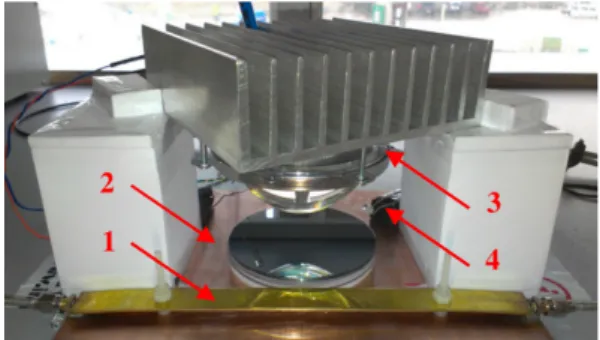
Figure 1: An experimental setup including a strip line (1), a WGM resonator (2), a heat sink with an LED and a light focusing lens (3), and a pin-diode photo-detector (4).
Figure 2: Schematic of a microwave WGM resonator [1].
though applied only to direct-gap semiconductors, which produce sufficient photoluminescence, e.g., GaAs. The µPCD methods measure the conductivity induced by light, which is proportional to the product of density and mobil-ity of charge carriers. They can be used with both direct-gap and indirect-direct-gap semiconductors, e.g., Si [5-7]. Both the techniques, being contactless methods, have essential benefits over other approaches, though they require high-power laser sources for creating significant photo-excitation and, typically, are implemented using expensive equipment made for industrial applications [4].
For advancing µPCD methods, an enhancement of the photoresponse was proposed based on the use of resonant circuits and structures. This resulted in the development of resonance coupled [8] and transmission modulated [9] photoconductive decay techniques, RCPCD and TMPCD, respectively, which showed a big improvement in the re-combination measurements despite the fact that the quality factor Q of the resonators was rather limited.
There are different mechanisms of electron-hole recom-bination, which may coexist, dominate, or replace one an-other, depending on the kind of semiconductor (direct- or indirect-gap), kind of doping (p- or n-type, degenerate or not, doped, undoped, or compensated), level of excitation (low or high) and other conditions [10]. The most com-mon are Shockley-Read-Hall recombination via impurity centers, radiative inter-band transitions, and Auger impact recombination, which are characterized by different depen-dencies on the electron-hole densities and different sets of recombination parameters.
In a broad range of circumstances, a generic concept of recombination lifetime can be introduced that corresponds to the exponential decay of carrier excitation in a semicon-ductor [11]. In practice, the relaxation may reveal a few exponential terms or show non-exponential decay. The re-laxation is more complicated when surface recombination is involved or barrier structures exist where carrier transport is essential. We consider undoped uniform semiconductor samples of relatively small thickness (∼ 0.5 mm) with no special surface treatment and barrier structures, though as-suming a possibility of surface recombination, which is a common property of Silicon samples [5-7].
Typically, it is difficult to measure recombination pa-rameters at low excitation level when the carrier density is on the order of 1015carriers/cm3, since the signal is low and
noisy, and the dynamic range is limited [5, 10]. So, most of the measurements for common semiconductors were made under high excitation conditions that correspond to 1016–
1017 carriers/cm3 and above. At the same time, the
low-excitation limit is of interest, since the recombination life-time is sensitive to the injection level. This is also the kind of condition that occurred in our experiments in [1, 2].
Despite the abundance of measurement techniques, we could not find any contactless method that would be suit-able for our Si wafers in a range of accessible laborato-ries around. In the meantime, trials of a more conven-tional technique (pressed-contact photoconductance) failed due to uncontrollable nonlinear effects of electron transport through unpredictable contact barriers and in the bulk of high-resistivity Si wafers. Besides, measurements of this kind require strong illumination that creates further prob-lems with this approach.
These circumstances created a stimulus for the devel-opment of a contactless measurement method that could be implemented in a laboratory using available technical means and equipment.
The aim of this work is to develop a resonance-enhanced WGM-based microwave photoconductivity method for contactless measurement of recombination lifetime in pure semiconductors and to apply it to the measurement of recombination lifetime in high-resistivity Si wafers. The advantage of the technique is the possibility of making measurements at low light intensity and low level of excitation of the semiconductor.
A novelty of the approach is the use of microwave WGM resonators with high quality factors [12], which
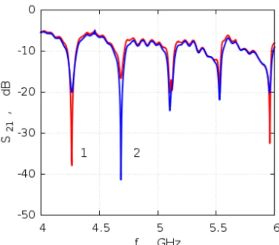
Figure 3: Transmission spectrum of a microwave WGM setup in the dark (curve 1) and in the light (curve 2).
greatly increases the sensitivity of a system that is based on conventional laboratory equipment. Should ultra-fast sub-THz Schottky barrier diodes be employed as millimeter-wave signal detectors [13], Si-loaded W-band Bragg res-onators [2] with greater Q factors at higher frequencies could be used for the detection of faster recombination pro-cesses producing much lower photoresponse.
2. Setup of the Whispering-Gallery-Mode
Photoconductivity-Decay Method
The method is based on the use of devices and components available in a typical RF laboratory. The main device is the R&S FSH8 Handheld Spectrum Analyzer (model .28 with FSH-K42 option) that operates as a vector network analyzer (VNA) in the frequency band f = 100 kHz – 8 GHz with a possibility of time-domain signal tracking at the chosen frequency (the best time resolution in this track-ing is ∆t = 1µs). High-resistivity Silicon wafers, depend-ing on their intended applications, may have the recombi-nation lifetime τRranging from nearly a second (ultra-pure
samples) to nano- and picosecond scales (radiation dam-aged wafers). For typical undoped Silicon, τRis likely to
be on a millisecond to microsecond scale that matches the time resolution of the VNA specified above.
The method utilizes the effect of resonant photosensitiv-ity of microwave transmission through a strip line coupled to the disk WGM resonator that contains a semiconductor layer [1]. The measurement system (Figs. 1, 2) consists of (1) a strip line suspended over a conducting plate, (2) a WGM resonator made of a set of dielectric and semicon-ductor wafers placed on the same plate, (3) a 100W blue or white LED array with a lens attached to the heat sink, and (4) a pair of pin-diode photo-detectors for measuring the light intensity, which is controlled by the LED array voltage VLED.
In order to operate at frequencies below 8 GHz, the resonator in this setup contains more dielectric wafers as compared to the WGM structure in [1]. The entire WGM
resonator consists of 7 MgF2 wafers placed on the copper
conducting plate, 9 sapphire wafers layed above (wafers of thickness 0.55 mm and 0.40 mm, respectively), and a top stack of a few Si wafers facing the LED. The top stacks were of the kinds: 3s1-2s2-LED (#1), 2s2-3s1-LED (#2),
1s1-LED (#3), and 1s2-LED (#4), where s1and s2are the
Si wafers specified above (alternatively, the entire resonator can be assembled from high-resistivity Si wafers).
The LED is controlled by an electronic switch provid-ing a fast (< 1µs) switchprovid-ing off the light pulse (faster than 0.2µs for the blue LED) and generating a synchronized trig-ger signal for the VNA operation. The strip line is con-nected to the VNA ports so that the microwave transmission signal is measured as a function of either the frequency f (over the given band at the fixed light intensity, Fig. 3) or the time t (at the chosen microwave frequency, when synchro-nized with an event of turning off the light pulse, Fig. 4).
3. WGM Enhanced Measurements of the
Photoconductivity Decay Times
Fig. 3 shows two kinds of resonances observed as the nar-row dips in S21that emerge either (1) in the dark state or
(2) under the light of the blue LED (the peak values of res-onator quality factors are Q ∼ 104, unlike Q ∼ 20 in an-other technique [3], but the resonator lifetime is still rea-sonably small, with an instant peak value being < 1.6µs). When setting the frequency in the time-domain measure-ments at the resonant point, we observe either the down-switch or the up-down-switch dynamics of S21 signals,
respec-tively (see Fig. 4, a and b). Some dips may have their min-imum at a medium light intensity. Then, we observe a hy-brid switch (Fig. 4, c) that corresponds to a system of twice greater sensitivity, thus improving the detection of small carrier density variations.
Figs. 5 – 7 show three kinds of result, which represent the main stages of the measurement process. The first result (Fig. 5) shows the transmission spectra S21(f ) of setup #3
as measured at different light intensities, which are related to cases (b) and (c) in Fig. 4.
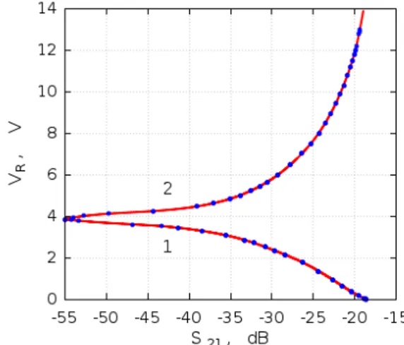
The second result (Fig. 6) is the calibration curve VR(S21) recovered from these spectra. The curve provides
the relationship between the light intensity presented by the photo-detector signal VR and the microwave transmission
signal S21, which is recorded under exactly the same
con-ditions (including the same frequency f0= 6.231000 GHz)
as used in the time-domain measurements of S21in Fig. 4,
b and c.
The third, and the main result (Fig. 7), is the actual time-domain curve VR(t) showing the recombination dynamics
of the photo-excited charge carriers (the effective photocon-ductivity, whose value is proportional to the VRlight signal,
i.e., the excess carrier density). The VR(t) signal is
recov-ered from the VNA measured S21(t) time-domain curve by
using the calibration function VR(S21) established above.
The S21(t) curve used in this procedure is found as an
average of 12 synchronized time-domain up-switch traces
(a)
(b)
(c)
Figure 4: VNA signal measured in the time-domain at the resonant frequency f0when turning off the light in the case
of (a) down, (b) up, and (c) hybrid switch in a setup with (a) WGM structure #1 (f0= 4.268882 GHz, VLED=32V)
and (b, c) WGM structure #3 (f0= 6.231000 GHz, VLED
=30.8V and 40.2V, respectively).
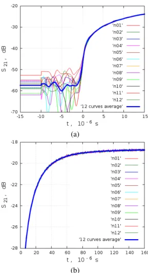
(Fig. 8) like those shown in Fig. 4, b. The traces were recorded repeatedly with sufficient intervals of dark-state relaxation between the light pulses. Fig. 8 illustrates the
Figure 5: Transmission spectra of setup #3 at different light intensities (VLED = 39, 33, 31, 30, 20V, curves 1 to 5,
re-spectively).
Figure 6: Calibration curve recovered from the data in Fig. 5 (branches 1 and 2 correspond to weak and strong light, respectively, dots show the measured values, and the curve is the smooth fit needed for data processing).
benefit of this averaging for computing more accurate rep-resentative curve S21(t) for further processing.
4. Simulations of the Photoconductivity
Decay in Semiconductor Wafers
Recovery of recombination parameters of Si wafers from the experimental data requires numerical simulations of the relaxation dynamics of photo-excited charge carriers after the turning off the optical excitation. The electron-hole dy-namics in Si wafers under the given conditions can be com-puted by using the drift-diffusion model of charge transfer in semiconductors under illumination [14].
In the case of high-resistivity Si wafers, we have to use the non-stationary electron-hole ambipolar diffusion equa-tion presented in the form
∂n ∂t − Da ∂2n ∂x2 + n − n0 τR = G(x, t) (1)
Figure 7: Time curves showing the recombination dynam-ics of photo-excited carriers (whose density is proportional to the light flux presented by the VRphoto-detector signal)
as recovered from the measured data (curve 1) and fitted with one-term and three-term exponential functions (curves 2 and 3, respectively), which show the dominant relaxation time τVR = 14µs (in case of s2wafers, τVR= 10µs).
where n = n0+ ∆n is the electron density in a
semi-conductor under illumination, n0 is the dark-state
equilib-rium electron density, ∆n is the excess density of non-equilibrium electrons created by photo-excitation, Da =
2DnDp/(Dn+ Dp) is the ambipolar diffusion coefficient,
Dnand Dpare the electron and hole diffusion coefficients,
τRis the electron-hole recombination lifetime, and G(x, t)
is the term describing the generation of the electron-hole pairs by the light flux. The wafer of thickness d is located at 0 ≤ x ≤ d. The light is incident on the wafer surface x = 0 while propagating in the positive x direction, which is normal to the wafer surface.
The generation term G(x, t) is computed as G(x, t) = g(t)
Z
l−1q (1 − r) exp (−x/l) dλ (2) where l = l(λ) is the length of light absorption in Si as a function of the wavelength λ [15], q = q(λ) is the quantum flux of light at the total power flux PL, r = r(λ) is the
reflection coefficient of light at the wafer surface, and g(t) is the function of time specifying the dynamics of photo-excitation.
The integral is taken over the range of wavelengths spe-cific for the given light source. We consider blue and warm-white LEDs radiating light at the wavelengths λ ∼ 450 nm (l ∼ 0.4µm) and λ ∼ 440 − 700 nm (l ∼ 0.4 − 5.3µm), respectively.
The function of time g(t) is chosen to define the light pulse of duration tP, which is turned on at t = −tP and
turned off abruptly at t = 0. The function is defined as g(t) = Θ(t + tP) − Θ(t) where Θ(t) is the unit step
func-tion.
The initial condition, imposed at t = −tP, is the
(a)
(b)
Figure 8: The S21(t) curve defined as an average of 12
syn-chronized up-switch traces when (a) −15µs ≤ t ≤ 15 µs and (b) 5 µs ≤ t < 160 µs.
Choosing the pulse duration tP ≥ 100µs, we achieve
a steady-state non-equilibrium carrier distribution estab-lished before t = 0 when the light is turned off and the simulation of photoconductivity decay started.
The boundary conditions at the wafer surfaces assume the finite speed S of surface recombination of charge car-ries. In practice, typically, the surface recombination is so high that nearly equilibrium carrier density is observed at the surfaces (n = n0at x = 0 and x = d).
The values of Da and τR define the electron-hole
am-bipolar diffusion length LR =
√
DaτR whose value
con-trols the distribution of photo-excited charge carries inside the wafers. At the given wafer thickness d, large values of LR (LR d) lead to significant redistribution of
photo-excited carriers across the wafer whereas a small LR
(LR d) supports the carrier profile as generated by the
local absorption of light.
Numerical solutions of Eqn. (1) were found for Si wafers for various values of the recombination parameters by using the FlexPDE simulation software. Simulation re-sults concerning the spatial distribution of photo-electrons in a Si wafer and the time decay curves of the total number
Figure 9: Decay of the photo-electron distribution in a Si wafer s1after the turning off the blue light with power flux
PL = 10 W/cm2at the moment t = 0 (curves 1 to 5 show
simulation results at the time t = 0, 1, 5, 10, and 20 µs, respectively, when τR= 6000 µs and τS = 0).
of electrons per unit area ntot(t) after the turning off the
light are presented in Figs. 9 – 11. The quantity ntot(t) =R
d
0 n(x, t)dx defines the
effec-tive photo-conductivity of the wafer σph(t) as σph(t) =
e(µn+ µp)ntot(t)/d where µn(p) is the electron (hole)
mobility and e is the elementary charge.
Fig. 9 shows the time decay of the photo-electron dis-tribution in the Si wafer s1 after the turning off the light
emitted by the blue LED with the initial power flux PL =
10 W/cm2. The results illustrate the process of redistribu-tion of charge carriers across the wafer along with the si-multaneous decay of carrier density in the sample that leads to the decay of total conductivity as detected in microwave experiments.
It is the comparison of these simulation results with relevant experimental data that allows one to extract the recombination parameters of wafers from a set of time-domain microwave photoconductivity experiments.
5. Extraction of the Recombination Lifetime
Parameters
For the comparison of simulated relaxation dynamics of charge carriers in a Si wafer and experimental VR(t)
photo-conductivity signal, we computed time decay curves ntot(t)
in a Si wafer for various values of recombination parame-ters. Then, by selecting the cases of the best fit between the measured and simulated curves, we identify those val-ues that allow us to better reproduce the experimental data VR(t).
Figs. 10 and 11 show some of ntot(t) curves found
at different values of the bulk and surface recombination times τR and τS, respectively, in a Si wafer of thickness
d = 0.5 mm (the wafer s1). The curves are presented in
relative units (curves 2 to 4) along with similarly normal-ized VR(t) experimental curves obtained above (curves 1 in
Figs. 7, 10, and 11).
Given the surface recombination speed S, the surface recombination time and length are defined as τS = Da/S2
and LS = Da/S, respectively, where Da = 18 cm2/s [14]
(LS =
√
DaτS). Then, the time parameters τR= 20, 666,
6000 µs and τS = 0.02, 0.056, 5.6, 35 µs that have been
tested in various combinations as possible parameter values (Figs. 9 – 11) correspond to the length parameters LR =
0.19, 1.1, 3.3 mm and LS = 0.006, 0.01, 0.1, 0.25 mm,
respectively.
For a quantitative analysis of time decay functions and comparison of simulation results with experimental data, we apply three-term exponential fitting of measured and simulated curves using the fitting function
η(t) =
3
X
k=1
ηkexp(−t/τk) (3)
where ηk is the contribution factor and τkis the relaxation
time of each term. The main term is the one that has the greatest contribution factor ηkthat, in turn, defines the main
relaxation time τk.
By fitting our data, we obtain the main relaxation times τVR = 14.4 µs, τ10.2 = τ11.2 = 14.5 µs, τ10.3 = 26 µs,
τ10.4 = 8.6 µs, and τ11.3 = 14.0 µs where the index VR
and the numerical indices α = 10.2, 11.2, . . ., correspond to the experimental function VR(t) and simulated curves in
Figs. 10 and 11, respectively.
Indices α = 10.2, 10.3, and 10.4 specify curves 2, 3, and 4 in Fig. 10. The curves are computed with the values of τR = 666 µs (curves 2 and 3) and τR = 20 µs (curve
4) when τS = 0.02 µs, τS = 5.6 µs, and τS = 0.056 µs
(curves 2, 3, and 4, respectively).
Indices α = 11.2 and 11.3 specify curves 2 and 3 in Fig. 11. These curves are obtained with the recombination parameters τR = 666 µs, τS = 0.02 µs and τR = 20 µs,
τS= 35 µs, respectively.
The main fitting terms have sufficiently large contri-bution factors ηVR = 0.84, η10.2 = η11.2 = 0.83,
η10.3 = 0.95, η10.4= 0.77, and η11.3= 0.96.
The pairs of τRand τSvalues used above constitute the
parameter sets Pαbeing tested. The pairs providing a good
match of simulated and experimental curves specify possi-ble values of recombination parameters being recovered.
The results presented above show the possibility of ex-tracting the recombination parameters of a Si wafer from the comparison of relaxation curves of measured and simu-lated photo-excitation in a semiconductor after the turning off the optical excitation.
The processing of experimental photoconductivity data reveals the main relaxation time to be τVR = 14.4 µs with
the contribution factor of the relevant term ηVR = 0.84.
The other terms are specified by parameters τ2 = 1.7 µs
and τ3= 59 µs at η2= 0.11 and η3= 0.05, respectively.
Simulations are capable of reproducing nearly the same value τ11.2 = 14.5 µs (curve 2 in Fig. 11) at the
recom-bination time parameters τR = 666 µs and τS = 0.02 µs
(S = 3 · 104cm/s), which specify the bulk and the surface
Figure 10: Decay of the total number of electrons in Si wafer s1after the turning off the blue light at t = 0 where
curve 1 presents experimental data and curves 2 to 4 show simulation results obtained at τR= 666 µs (curves 2 and 3)
and τR= 20 µs (curve 4) when τS = 0.02 µs, τS = 5.6 µs,
and τS = 0.056 µs (curves 2, 3, and 4, respectively).
Figure 11: Decay of the total number of electrons in Si wafer s1after the turning off the blue light at t = 0 where
curve 1 shows experimental data and curves 2 and 3 show simulation results at τR = 666 µs, τS = 0.02 µs and
τR= 20 µs, τS = 35 µs, respectively.
processes, respectively. Notice, however, that values close to the same relaxation time can be obtained (though, with a greater mismatch of curves) by using quite different recom-bination parameters, e.g., τ11.3= 14.0 µs with τR= 20 µs
and τS = 35 µs.
The reason for such a situation is that, at the given thick-ness of a Si wafer d, the charge carrier diffusion from the bulk to the wafer surfaces occurs at about the same time as measured in the experiment. At the initial carrier distribu-tion presented in Fig. 9, this time is found, approximately, as τD ≈ (d/3)2/Da ≈ 15 µs. In case of τS < τD < τR,
it is the time τD that defines the relaxation time detected
in the experiment. About the same relaxation time is also obtained when τS ∼ τR ∼ τD. In this case, the process is
controlled by all the time parameters being involved. Re-moving this ambiguity requires either much thicker wafers or significant suppression of surface recombination.
In practice, undoped Si is, usually, characterized by a large recombination lifetime, e.g., τR = 666 µs as
mea-sured in the float-zone Si wafers [8]. At the same time, the surface recombination in Si is, usually, very fast, if no special treatments applied. The FZ Si wafers in our ex-periments are of this kind. In this case, the measured re-laxation time τVR is the effective quantity representing the
entire sample rather than the material parameter. Nonethe-less, the relaxation time τVR is valuable as an engineering
design parameter.
6. Conclusions
A resonant microwave-detection photoconductivity-decay method has been proposed for contactless recombination lifetime measurements in semiconductor wafers. The method utilizes microwave whispering-gallery-mode disk resonator structures, which can provide large quality fac-tors Q ∼ 104 for resonances and, therefore, a large en-hancement of the sensitivity of the measurement system.
The method allows one to measure recombination life-times τRat a very low level of excitation (∆n < 1015cm−3
at PL < 10 W/cm2) and use inexpensive LED arrays as
the light sources. The method has been used for mea-suring recombination parameters in high-resistivity float-zone Si wafers (ρ ∼ 5 − 30 kOhm·cm) with wafer thick-ness d ∼ 0.4 − 0.5 mm, which show the relaxation times τ ∼ 10 − 14 µs, respectively.
In wafers of small thickness under the typical condition of slow bulk and rapid surface recombination, the measured relaxation time is defined by the electron-hole diffusion to wafer surfaces rather than the bulk recombination rate.
When using wafers of greater thickness or reducing the rate of surface recombination, one can measure the bulk recombination lifetime directly, with high sensitivity, and in a broad range of light intensities, which is hard to achieve with other techniques.
Acknowledgement
The work was supported by The Scientific and Technolog-ical Research Council of Turkey (TUBITAK) through the 2221 Fellowship Program for Visiting Scientists and Scien-tists on Sabbatical Leave (2017/2).
References
[1] V. Yurchenko, M. Ciydem, A. Altintas, Light-controlled microwave whispering-gallery-mode quasi-optical resonators at 50W LED array illumination, AIP Adv. 5: 087144, 2015.
[2] V. Yurchenko, M. Ciydem, M. Gradziel, A. Mur-phy, A. Altintas, Light-controlled photonics-based mm-wave beam switch, Opt. Express 24: 15: 16471, 2016.
[3] M. Kunst, G. Beck, The study of charge carrier ki-netics in semiconductors by microwave conductiv-ity measurements, J. Appl. Phys., 60: 355–3566, 1986.
[4] G. Beck, M. Kunst, Contactless scanner for pho-toactive materials using laser-induced microwave absorption, Rev. Sci. Instrum. 57: 197–201, 1988. [5] D. C. Gupta, F. R. Bacher, W. M. Hughes, Eds.,
Recombination Lifetime Measurements in Silicon, ASTM special technical publication, 1340: 1–392, 1998.
[6] O. Palais, A. Arcari, Contactless measurement of bulk lifetime and surface recombination velocity in silicon wafers, J. Appl. Phys. 93: 4686–4690, 2003. [7] K. Lauer, A. Laades, H. ¨Ubensee, H. Metzner, A. Lawerenz, Detailed analysis of the microwave-detected photoconductance decay in crystalline sil-icon, J. Appl. Phys. 104: 104503, 2008.
[8] R.K. Ahrenkiel, S.W. Johnston, Resonant coupling for contactless measurement of carrier lifetime, IEEE 39th PV Specialists Conference, 1389–1393, 2013.
[9] R. K. Ahrenkiel, D. J. Dunlavy, A new lifetime di-agnostic system for photovoltaic materials, Sol. En-ergy Mater. Sol. Cells95: 1985–1989, 2011. [10] W. K. Metzger, D. Albin, D. Levi, P. Sheldon, X. Li,
B. M. Keyes, and R. K. Ahrenkiel, Time-resolved photoluminescence studies of CdTe solar cells, J. Appl. Phys.94: 5: 3549–3555, 2003.
[11] D. K. Schroder, The concept of generation and recombination lifetimes in semiconductors, IEEE Trans. Electron Devices, 29: 8: 1336–1338, 1982. [12] A. Barannik, N. Cherpak , A. Kirichenko, Y.
Prokopenko, S. Vitusevich, V. Yakovenko, Whis-pering gallery mode resonators in microwave physics and technologies, Int. J. Microwave Wire-less Technolog.9: 4: 781–796, 2017.
[13] N. W. Chen, J.-W. Shi, H.-J. Tsai, J.-M. Wun, F.-M. Kuo, J. Hesler, T. W. Crowe, J. E. Bowers, Design and demonstration of ultra-fast W-band photonic transmitter-mixer and detectors for 25 Gbits/sec error-free wireless linking, Opt. Express 20: 19: 21223, 2012.
[14] S.M. Sze, Semiconductor Devices, Physics and Technology, John Wiley and Sons, Hoboken, NJ, 2002.
[15] M.A. Green, M.J. Keevers, Optical properties of in-trinsic silicon at 300 K, Prog. Photovoltaics Res. Appl.3: 3: 189–192, 1995.