Band-Bending at Buried SiO
2
/Si Interface as Probed by XPS
Mehmet C
̧opuroğlu,
†Hikmet Sezen,
†Robert L. Opila,*
,‡and Sefik Suzer*
,††Department of Chemistry, Bilkent University, 06800 Ankara, Turkey
‡Departments of Materials Science and Engineering, University of Delaware, Newark, Delaware 19716, United States
ABSTRACT: X-ray photoelectron spectroscopy is used to probe the photoinduced shifts in the binding energies of Si2p, O1s, and C1s of the SiO2/Si interfaces of a number of samples having oxide and/or thin organic layers on top of p- and n-Si wafers. Whereas the photoinduced shifts, in each and every peak related, vary from 0.2 to 0.5 eV for the p-type samples, the corresponding shifts are substantially smaller (<0.1 eV) for the n-type, regardless of (i) oxidation route (thermal or anodic), (ii) thickness of oxide layer, (iii) nature of organic layer, or (iv) color of three illuminating sources we have used. This leads us to conclude that these particular photoshifts
reflect the charge state of the SiO2/Si interface, even in the case of a 20 nm thick oxide, where the interface is buried and cannot
be probed directly by XPS.
KEYWORDS: band-bending, buried interface, photovoltage, XPS, doping
■
INTRODUCTIONChemical and electronic interactions at surfaces and interfaces of semiconductors are crucial for performance of electrical devices, photovoltaics, and photocatalytic reactions, and for proper interpretation of surface analyses. Because surfaces and interfaces are invariably imperfect, lattice defects, chemical impurities, and dangling bonds are often present. At thermodynamic equilibrium, the electrochemical potential must be constant as a function of depth even in the presence of these imperfections. Thus, the electrochemical potential must reflect the presence of chemical or lattice defects at the surface or interface. As a result bending of the valence and conduction bands occurs as a function of depth in the sample away from the surface or interface.1 Zhang and Yates have recently reviewed many of the manifestations of this “band bending”.2
Electronic band bending is interesting because it is an area where purely physical forces, such as externally applied potentials or deposition of electronic charges, can have immediate chemical input. For example, many authors have proposed chemical field effect transistors, where specific chemical reactions, occurring at the surface of a semiconductor, bend the bands of the substrate materials, thereby changing the conductivity of the substrate dramatically, and permitting in situ amplification of the chemical signal.3−5 Along the same line, utilization of band-bending for (i) increasing osteoblast adhesion to hydroxyapatite,6 (ii) boosting photocatalytic activity of TiO2 by modifying with Ag nanoparticles,
7
(iii) controlling the ionization energies of capped CdSe nanocryst-als,8 (iv) valence band-edge engineering of NiO nanoparticles by Co doping,10 (v) incorporation of electrochemically and photochemically active moleculer interfaces to SnO2surfaces,
10
and (vi) tuning heterostructure functionality of SiC surfaces by
different organaosilanes, have recently been demonstrated.11A very recent paper reports on patterning of silicon surfaces by assembly of metal nanoparticles for applications in photo-electroctalysis.12
In this paper, we will show how electron spectroscopies, particularly core level X-ray photoelectron spectroscopy (XPS) is ideal to probe the chemical and electronic states of a surface or interface simultaneously. In fact, XPS can be used to characterize a buried interface that is deeper than the escape depth of the photoelectrons (typically 10 nm), but is sampled by the incident light, which is transmitted to depths of 100 nm or more.13−15Exposure of materials to light leads to a number of physical and chemical changes on materials, most notably to generation of electrical potentials, commonly referred as photovoltage or surface photovoltage, SPV, which can also be probed by XPS.16Si2p core levels are excellent for determining the energies of valence band maxima because they are sharp and their shifts are identical to shifts in the band edges in cases of band bending and the application of external potentials.17,18 In our previous work, we examined the photoinduced binding energy shifts in n-type and p-type Si wafers with and without oxide layers.19 Without light exposure, the energy difference between the p-type and n-type Si2p peaks on H-terminated surfaces was 0.18 eV, and upon light exposure, the p-type Si2p shifted to lower binding energies (greater kinetic energies), and the n-type to higher, resulting in a larger difference of 0.49 eV, very close to the flatband condition. Moreover, we observed that, with illumination, the difference between the Si0and Si4+2p peaks for p-type and n-type Si was
Received: May 6, 2013
Accepted: June 4, 2013
Published: June 4, 2013
Research Article
conserved even when a thin oxide was grown on the surface, and the Si2p peak for p-type Si shifted more under light exposure (hv > 1.12 eV) than the corresponding n-type peak. This finding was postulated to be due to a combination of band-bending and positively charged silicon oxide interface, such that the result was additive in the shifts for the p-Si/SiO2
interface and subtractive for the n-Si/SiO2 case. The present contribution dwells on the same findings with more and comprehensive additional experimental evidence in support of our postulate.
Note also that it is well established that during XPS analysis of nonconducting samples or surface structures positive charges are created due to photoemission process, the extent of which depends on many parameters like, the chemical nature, synthesis conditions, as well as the thickness of the layers, etc. This kind of charging is easily controlled and compensated for by use of low energy electron and/ion sources.31,34,35 Indeed, all of the silicon oxide layers investigated in the present work are positively charged, as evidenced by the measured positions of the corresponding peaks. However, this phenom-enon is not within the scope of the present work, where we concentrate on shifts observed due only to light illumination. Our ongoing work includes investigation of the complex photo shifts together with the charging ones, and our attempts to entangle the two, which will be the subject of a future publication.
■
EXPERIMENTAL SECTIONA Thermo Fisher K-Alpha electron spectrometer with monochromatic Al Kα X-rays was used, with an overall accuracy of 0.02 eV in the binding energy shifts. Three CW solid-state lasers with an average rated power of ∼50 mW at 635, 532, and 405 nm were used for illumination. The lasers were focused on the specimen surface through a quartz window and mechanically shuttered. The spectrometer is
equipped with a low energyflood gun that can utilize either electrons or electrons and Ar ions. In the work reported, generally, theflood gun was not used unless otherwise stated. An external power supply (Stanford Research System DS 340 pulse generator) was used to apply ±10 V square wave pulses (unity duty cycle) with frequencies in the range 10−3to 105Hz. At low frequencies (0.001 Hz), the Si4+2p of the oxide layer shifts less than±10 eV, because the layer is allowed to charge and discharge, but at high frequencies (>100 Hz), the shift is exactly±10 V, since not enough time is allowed.20
Commercially available p- and n-type Si(100) wafers were used, with conductivities of 10−20 and 28−31 Ω-cm and doped with B and P, respectively. The wafers were cleaved into ∼1 cm squares, and dipped into concentrated (Merck, 38−40%) HF, rinsed with deionized water (DI H2O), and acetone, then blown dry. The HF dip and subsequent dips were repeated three times total. Oxides were grown under air in an oven at 700 °C for three hours. Anodically grown oxides were also investigated. These oxides were grown in a dilute 0.01 M NaCl solution with identical cathodes and anodes, after the HF etching. A current of 20 mA was passed between the electrodes and bubbles were observed on the anode. The applied voltage was approximately 100 V during this process. The oxide was patchy and grown in approximately 20−60 min for the p- and n-type specimens, respectively with an estimated thickness of >15 nm. Depth profiling was conducted using 500 eV Ar+ions with a nominal current density of∼20 μA/cm2.
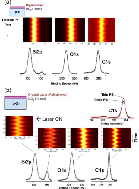
Polystyrene and n-hexane were deposited on H-terminated and thermally oxidized surfaces for providing spectator overlayers. The polystyrene was dissolved in chlorobenzene (Sigma-Aldrich research grade) at room temperature and spin-coated on the prepared chip surface at 2000 rpm for 30 s. Previously,films prepared under these conditions were approximately 20 nm thick.29The polystyrene layers were thinned by dipping the polystyrene coated samples in chlorobenzene at room temperature for 60 s. The ratio of theπ−π* shake-up intensity to the core C1s feature is approximately the same before and after rinsing, suggesting that most of the residual carbon-containing species on the surface is polystyrene. Only the specimens with the thin layers of polystyrene were used to minimize effects of charging and to be able to see the O1s and Si2p peaks of the Figure 1.From left to right the Si2p3/2, 1/2peaks for H-terminated n- and p-type Si and thermally oxidized Si with a∼6 nm oxide layer on top, and the O1s peaks of the oxide layer with violet laser on and off. Peak shifts for the Si2p3/2are noted explicitly. In the top, the time evolution of the O1s peak of the p-type Si oxide is plotted as the laser is strobed, where yellow is the most intense region in the O1s spectrum and black reflects the background.
underlying SiO2and Si. No Cl features, after the chlorobenzene rinse, was observed in the survey spectra. The hexane (Merck, EMPLURA) was deposited on the prepared surfaces by dipping into solutions at room temperature for 60 s.
For estimation of the thicknesses of the oxide or other layers, the well-established procedures, based on the intensity of the correspond-ing peaks corrected for their attenuation lengths, are used or adopted.30,31We estimate the accuracy in thickness determination to be±1 nm.
Mechanically chopping the laser shows that on the time scale of the experiment (τ < 0.1 s), the contribution of light generated charged carriers to maintainflattened bands is a faster process. When a charge neutralizer (low energy source of electrons and positive Ar ions) is used, the low energy charged particles neutralize any charge that generates an electricfield at the surface. The time constant for this neutralization process can be slow (seconds to tens of minutes), at a rate given by the diffusion and drift of charges from the source.21,22In addition, the external charges are not expected to be sensitive to charges at the Si/oxide interface that is compensated by band bending (the net potential far from the interface will be zero). On the other hand, carriers generated internally by a light source will be sensitive to the presence of charge at the interface, and will respond at times much more quickly.23−28
■
RESULTSIn Figure 1, the shift in Si 2p peak for both p-type and n-type Si with the 405 nm laser off and laser on are shown, which is essentially the same as reported in our previous paper.19The shift upon illumination in the 2p3/2 peak for p-type is
approximately 0.19 eV, and for n-type is 0.11. The difference in binding energy for the n-type and p-type H-terminated Si with the light on is 0.49 eV. Upon introduction to the spectrometer, electrons flow from the n-type and holes from the p-type Si wafers so that they are charged differently, due to doping. However, the charges on the surfaces are screened by band bending and by accumulation of opposite-sign charges near the surface.13−15 When light of energy greater than the band gap of Si is incident on the sample charge carriers return the bands to the flat-band condition.30−33 This data was collected with neutralizer off. We also modulated (not shown here) the electrical potential of the surface using an external
power supply generated square waves of±10 V amplituted and at frequencies from 0.5 to 500 Hz, with no observable effect on the shifts due to the incident light.
Essentially the same behavior was observed for the O1s, Si0
2p3/2, and Si4+2p
3/2peaks for the thermally oxidized silicon. In
the inset of Figure 1, only the O 1s peak of the p-type silicon sample is plotted as a function of time while the 405 nm laser is alternately blocked. The peaks shift 0.4 eV to lower binding energy for p-type Si when the laser is incident, in parallel but larger than shift of the p-type H-terminated Si surface. These results, again, were acquired with the neutralizer off. Transitions for the n-type Si are much smaller.
We note in passing that the snapshot types of measurements, as shown in the inset of Figure 1, which is used for most of the data reported in this paper, are more accurate for measuring photoshifts, when compared to longer conventional region scans, since the former eliminates the unwanted effects of instrumental instabilities or drifts. Second, in addition to abrupt photoshifts, slight changes with time both in the Si2p4+ and O1s position of the oxide layer are also observable. These slower shifts are the result of additional neutralization of the positive charges on the oxide layer by the incident light. Such changes are observable in all the nonconductiong moieties, like the oxide layer as well as the thin organic layers investigated, but as was mentioned earlier, these issues will not be discussed any further in this contribution.
In addition, as depicted in Figure 2, there is no significant dependence on the energy of the lasers used to cause the shift in the position of the O1s peak for the lasers at wavelengths 635, 532, and 405 nm. Recall that all lasers had approximately
the same power (∼50 mW) and were focused onto
approximately the same size. Moreover, all lasers have energies greater than the band gap of Si. In separate experiments, the fluency dependence of the observed photoshifts were checked by inserting neutral optical densityfilters and to ensure that all are to be above saturation.
Interestingly, similar results were seen for thick thermal and anodic oxides. Here, mean probe depth of XPS is approximately Figure 2.Time evolution of the O1s peak of p- and n-type Si with a∼6 nm oxide layer on top, as the three lasers are strobed.
10 nm, given by three times the mean free path (∼3 nm) of the generated photoelectrons. Yet, the thick thermal and anodic oxides on p-type Si are∼20 and >15 nm thick. Figures 3a and 3b show that the shifts of the Si4+2p and O1s are virtually the
same as those of the thin thermal oxide sample.
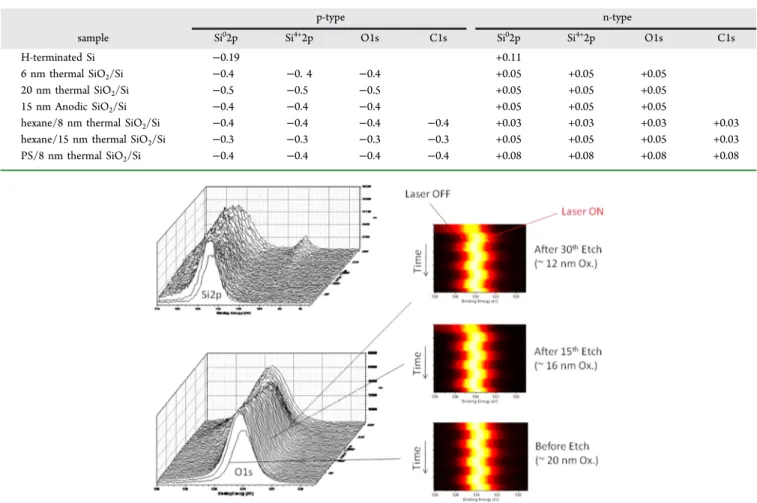
Wafers with ∼8 nm thick thermally grown oxides were dipped into hexane and blown dry. As shown in Figure 4a, the Si2p and the O1s from the SiO2layer, and the C1s from the hydrocarbon residues respond identically to illumination of the p-type substrates. Again, the responses for the n-type wafers (not shown here) are substantially smaller than the response for the p-type wafers.
These experiments were repeated for thermally oxidized Si surfaces coated with polystyrene and thinned by briefly dipping into chlorobenzene. Measurable quantities of polystyrene remained on the surface as shown in the C1s spectrum. Note that the ratio of theπ−π* shake-up intensity to the core C1s feature is approximately the same before and after rinsing, suggesting that most of the residual carbon-containing species on the surface stem from polystyrene.34 The residual polystyrene C1s, as well as Si4+2p and O1s responded identically to the hydrocarbon residue films, as shown in the inset of Figure 4b. Again, the illuminated XPS experiment can directly sample the underlying substrate even though there are few emitted photoelectrons from that depth. The processes are schematically shown in Figure 5, and relevant data are collected in Table 1.
The affect of the surface photovoltage from the contribution of light-generated carriers can be generalized. We looked at the shift on illumination of the∼20 nm thick thermal oxide as a function of depth, profiled by Ar+ ion sputtering. In Figure 6 the O1s and Si4+2p regions are shown as a function of sputter
cycles (the specimen is alternately sputtered and the XPS data is acquired). While the absolute position of the O1s and Si2p peaks appear to drift as a function of depth, the photovoltage shift in the O1s peak position as a function of light illumination does not.
■
DISCUSSIONBand bending occurs at surfaces and interfaces so that the electrochemical potential or Fermi level can remain continuous across that surface or interface. As a result of the band bending there is an increase, or decrease, of electronic charge as one approaches the interface. Valence and conduction bands at surfaces of p-type semiconductors typically bend to lower energy as a result of reduced number of negative charge density compare to their bulk, and bend to higher energies at n-type surfaces.17,18 Rapid recombination of charge carriers at the surface or interface will prevent accumulation of charges. Introduction of extra charge carriers by illumination at a rate greater than the recombination rate will cause charge to accumulate and the bands toflatten.
In our experiments, we have looked at the surface photovoltage shift for a series of surfaces and interfaces using XPS. The important feature in this measurement is that XPS probes only 3−12 nm, but the incident light can penetrate perhaps a micrometer. We determined the SPV for H-terminated Si surfaces, thermally and anodically oxidized surfaces, and finally oxidized surfaces with a thin polystyrene film and following a hexane dip. The surface photovoltage was studied with three different lasers, with an average rated power of∼50 mW at 635, 532, and 405 nm. Each of these lasers has an energy greater than the bandgap of Si, and enough intensity to saturate the process. In addition, external voltages were applied. In all of these cases, essentially the same SPV was observed for each of the peaks monitored (e.g., Si2p, O1s, or C1s) for a given doping. Furthermore, externally applied±10 V square wave pulses (unity duty cycle) with frequencies in the range 0.5 to 500 Hz were applied. Both positive and negative sweeps gave the same SPV, and the SPVs were in essential agreement with those found under static conditions. Application of an external voltage causes the overall Fermi level of the specimen to increase or decrease, but, in the absence of a neutralizing source of electrons or light, will not affect the band bending at the surface. If there are electrically charged moieties at the surface, an external flood gun may neutralize these charges. However, as these charged entities induce a band bending, thereby essentially forming a dipole, the effective field felt by the impinging electrons and ions may be small. In the case of an insulator, or an intrinsic semiconductor, there may not be enough free charge carriers in the specimen to neutralize the charges, thereby making the external neutralizer more effective. Thus, the response of the semiconducting surface to a neutralizer will vary from specimen to specimen.
Different SPVs were observed for H-terminated and the oxidized specimens. For example, for p-type Si with H-termination was 0.19 eV. The shift observed for the O1s and Si4+2p SPV for a thin thermal oxide is on the order of 0.5 eV. However, for H-terminated n-type Si, the SPV is 0.11 eV, while the SPV for the oxide measured at O1s and Si4+2p is less than Figure 3.Changes in the O1s peak for the p-Si as the Violet Laser is
strobed: (a)∼20 nm Thermal Oxide, (b) >15 nm Anodic Oxide.
0.05 eV, 1 order of magnitude smaller. All of these observations must be related with the composition of the oxide-Si interface, and the fact that both the oxide and the substrate peaks exhibit more or less the same SPV shifts signifies that they are strongly correlated with the interface. The important question arises as to the cause of this significant asymmetry between the p- and the n-Si/oxide interfaces, as we will now try to answer.
It is well established that the oxide side of the interface is positively charged as the result of electron injection to the silicon side for any type of silicon, as schematically shown in Figure 7.16,30−33 Hence, as was already advocated in our previous publication, the overall band-bending is additive (p-type + oxide), resulting in a larger shift (∼0.5 eV) upon illumination.19The absence of significant photoshift for the n-sample, can also be attributed to compensation of the surface upward bending of the n-Si by the oxide downward bending at the interface, as schematically shown in Figure 7b. This point is our postulate and naturally is open for debate.
Moreover, the SPV observed for the thermal oxide, thinned polystyrene on thermal oxide, and hexane-dipped thermal oxide Figure 4.(a) Changes in the Si2p and the O1s peak of the p-Si with a∼8 nm thermal oxide, dipped into hexane and blown dry. Changes in the C1s of the organicfilm is also shown. (b) Similar sample but containing a thinned Poly-styrene (PS) film on top. The inset shows the C1s region of a ∼20 nm (thick) and thinned PS films.
Figure 5.Schematics of the processes described for the p-type Si-wafer having a thick silicon oxide (∼20 nm) and an organic layer (∼2 nm) on top. XPS probes only the top∼12 nm of the surface, but the laser illumination can reach the interface (∼22 nm), as well as the space-charge region (∼100 nm). Upon illumination bending of the p-Si is flattened and the interface charges are nearly eliminated. The resulting interface photovoltage change can be probed both in the spectator organic and the oxide layers.
specimens should all yield identical results because the only interface with band bending accessible with visible light generated charge carriers is the SiO2/Si interface. In this case
XPS under illumination is probing the electrical properties of an interface undetectable by the photoelectrons. Differences between the anodically and thermally grown oxides might be expected because of differences in the SiO2/Si interfaces for
these two examples. However, in this experiment no differences were seen. On the other hand, differences at the interface between high-k oxides and the Si substrate would be expected to be evident in the SPV.35In fact, certain choices of the high-k,
might result in different magnitudes in the SPV, or even, in the sign of the SPV.
The time evolution of SPV can be estimated by knowing the number and mobility of the charge carriers. For example, if more charge carriers are generated, the surface voltage should be generated faster. In addition, if the charge carrier mobility is greater, the SPV should be generated more quickly. The time scale of external generated voltage is governed by the time constant of the circuit including any dielectric in the specimen, and the timing of voltages generated by neutralizers will be on the scale of the diffusion of electrons and ions in the vacuum. Band bending and the surface photovoltage can have myriad implications. First, the SPV provides an opportunity for a surface sensitive technique like XPS to probe a buried interface. Thus, synchrotron measurements of band banding may underestimate the effect of band bending by introducing a built-in SPV. Understanding how the band bending responds to the presence of external charges may make design of a chemically switched field effect transistor more effective. Similarly, photocatalysis, and photoelectroctalysis can be improved by optimizing the band banding for that particular reaction. Changes in silicon surface chemistry might also be expected to be influenced by SPV by introducing a reservoir of excess electrons (or holes) at the surface that may be actively used for chemically reducing (or oxidizing) nearby molecules. Table 1. Measured Binding Energy Shifts (SPV) in eV, upon Illumination with CW∼50 mW Red (635 nm), Green (532 nm), and Violet (405 nm) Lasers
p-type n-type
sample Si02p Si4+2p O1s C1s Si02p Si4+2p O1s C1s
H-terminated Si −0.19 +0.11
6 nm thermal SiO2/Si −0.4 −0. 4 −0.4 +0.05 +0.05 +0.05
20 nm thermal SiO2/Si −0.5 −0.5 −0.5 +0.05 +0.05 +0.05
15 nm Anodic SiO2/Si −0.4 −0.4 −0.4 +0.05 +0.05 +0.05
hexane/8 nm thermal SiO2/Si −0.4 −0.4 −0.4 −0.4 +0.03 +0.03 +0.03 +0.03
hexane/15 nm thermal SiO2/Si −0.3 −0.3 −0.3 −0.3 +0.05 +0.05 +0.05 +0.03 PS/8 nm thermal SiO2/Si −0.4 −0.4 −0.4 −0.4 +0.08 +0.08 +0.08 +0.08
Figure 6.O1s and Si2p spectra of a the p-Si wafer having a∼20 nm thick oxide layer, as a function of Ar+ etching for dept-profiling. On the right-hand-side, changes in the O1s peak are given at three different depths.
Figure 7.Schematic representation of band-bending for p- and n-Si containing an oxide layer on top. B.E. and K.E. refer to binding and kinetic energies, respectively.
■
CONCLUSIONSThe effect of surface photovoltage on the shifts of semi-conductor core levels has been studied. Shifts in the core levels follow shifts in the valence band maxima and the conduction band minima. Surface photovoltage, induced by incident photons with energy greater than the band gap, flattens the bands. Surface photovoltage can be used to understand the quality of surfaces and interfaces, and can be separated from the effects of externally applied voltages and external neutralizing sources. Since the light penetrates much deeper into the specimen than the acquisition depth of photoelectrons, SPV offers a method to probe the electrical nature of buried interfaces.
■
AUTHOR INFORMATION Corresponding Author*E-mail: [email protected] (R.L.O.); [email protected] (S.S.).
Notes
The authors declare no competingfinancial interest.
■
ACKNOWLEDGMENTSThis work was partially supported by TUBITAK, through the Grant No: 211 T 029. R.L.O. would like to acknowledge support of Fulbright Foundation, supporting his visit to Bilkent University for the Fall 2012 semester.
■
REFERENCES(1) Zhang, X. G. Electrochemistry of Silicon and Its Oxide; Kluwer Academics: Plenum, NY, 2001.
(2) Zhang, Z.; Yates, J. T. Chem. Rev. 2012, 112, 5520−5551. (3) Forzani, E. S.; Li, X.; Tao, N. Anal. Chem. 2007, 79, 5217−5224. (4) Vehoff, T.; Chung, Y. S.; Johnston, K.; Troisi, A.; Yoon, D. Y.; Andrienko, D. J. Phys. Chem. C 2010, 114, 10592−10597.
(5) Teo, B. K.; Sun, X. H. Chem. Rev. 2007, 107, 1454−1532. (6) Nakamura, M.; Nagai, A.; Hentunen, T.; Salonen, J.; Sekjima, Y.; Okura, T.; Hashimoto, K.; Toda, Y.; Monma, H.; Yamashita, K. ACS Appl. Mater. Interfaces 2009, 1, 2181−2189.
(7) Wodka, D.; Bielariska, E.; Socha, R. P.; Elzbieciak-Wodka, M.; Gurgul, J.; Nowak, P.; Warszyriski, P.; Kumakiri, I. ACS Appl. Mater. Interfaces 2010, 2, 1945−1953.
(8) Munro, A. M.; Zacher, B.; Graham, A.; Armstrong, N. R. ACS Appl. Mater. Interfaces 2010, 2, 863−869.
(9) Natu, G.; Hasin, P.; Huang, Z.; Ji, Z.; He, M.; Wu, Y. ACS Appl. Mater. Interfaces 2012, 4, 5922−5929.
(10) Benson, M. C.; Ruther, R, E; gerken, J. B.; Rigsby, M. L.; Bishop, L. M.; Tan, Y.; Stahl, S. S.; Hamers, R. J. ACS Appl. Mater. Interfaces 2011, 3, 3110−3119.
(11) Schoell, S. J.; Sachsenhauser, M.; Oliveros, A.; Howgate, J.; Stutzmann, M.; Brandt, M. S.; Frewin, C. L.; Saddow, S. E.; Sharp, I. D. ACS Appl. Mater. Interfaces 2013, 5, 1393−1399.
(12) Fabre, B.; Hennous, L.; Ababou-Girard, S.; Meiadec, C. ACS Appl. Mater. Interfaces 2013, 5, 338−343.
(13) Demuth, J. E.; Thompson, W. J.; DiNardo, N. J.; Imbihl, R. Phys. Rev. Lett. 1986, 56, 1408−1411.
(14) Halas, N. J.; Bokor, J. Phys. Rev. Lett. 1989, 62, 1679−1682. (15) Long, J. P.; Sadeghi, H. R.; Rife, J. C.; Kabler, M. N. Phys. Rev. Lett. 1990, 64, 1158−1161.
(16) Kronik, L.; Shapira, Y. Surf. Sci. Rep. 1999, 37, 1−206. (17) Kraut, E. A.; Grant, R. W.; Waldrop, J. R.; Kowalczyk, S. P. Phys. Rev. Lett. 1980, 44, 1620−1623.
(18) Himpsel, F. J.; Hollinger, G.; Pollak, R. A. Phys. Rev. B 1983, 28, 7014−7018.
(19) Sezen, H.; Suzer, S. J. Chem. Phys. 2011, 135, 141102−4.
(20) Suzer, S.; Sezen, H.; Ertas, G.; Dana, A. J. Electron Spectrosc. Relat. Phenom. 2010, 176, 52−57.
(21) Sezen, H.; Ozbay, E.; Aktas, O.; Suzer, S. Appl. Phys. Lett. 2011, 98, 111901−3.
(22) Sezen, H.; Suzer, S. Surf. Sci. 2010, 604, L59−L62.
(23) Marsi, M.; Nahon, L.; Couprie, M. E.; Garzella, D.; Hara, T.; Bakker, R.; Billardon, M.; Delboulbe, A.; Indlekofer, G.; Taleb-Ibrahimi, A. J. Electron Spectrosc. Relat. Phenom. 1998, 94, 149−157.
(24) Widdra, W.; Brocker, D.; Giessel, T.; Hertel, I. V.; Kruger, W.; Liero, A.; Noack, F.; Petrov, V.; Pop, D.; Schmidt, P. M.; Weber, R.; Will, I.; Winter, B. Surf. Sci. 2003, 543, 87−94.
(25) Marsi, M.; Couprie, M. E.; Nahon, L.; Garzella, D.; Bakker, R.; Delboulbe, A.; Nutarelli, D.; Roux, R.; Visentin, B.; Grupp, C.; Indlekofer, G.; Panaccione, G.; TalebIbrahimi, A.; Billardon, M. Nucl. Instrum. Meth, A 1997, 393, 548−551.
(26) Marsi, M.; Couprie, M. E.; Nahon, L.; Garzella, D.; Hara, T.; Bakker, R.; Billardon, M.; Delboulbe, A.; Indlekofer, G.; Taleb Ibrahimi, A. Appl. Phys. Lett. 1997, 70, 895−897.
(27) Marsi, M.; Belkhou, R.; Grupp, C.; Panaccione, G.; Taleb-Ibrahimi, A.; Nahon, L.; Garzella, D.; Nutarelli, D.; Renault, E.; Roux, R.; Couprie, M. E.; Billardon, M. Phys. Rev. B 2000, 61, R5070− R5073.
(28) Brocker, D.; Giessel, T.; Widdra, W. Chem. Phys. 2004, 299, 247−251.
(29) Sezen, H.; Ertas, G.; Dana, A.; Suzer, S. Macromolecules 2007, 40, 4109−4112.
(30) Birer, O.; Sayan, S.; Suzer, S.; Aydinli, A. J. Mol. Struct. 1999, 480−481, 611−614.
(31) Briggs, D.; Seah, M. P. 2, Practical Surface Analysis, 1, Wiley: Chichester, U. K., 1996.
(32) Hirose, K.; Nohira, H.; Azuma, K.; Hattori, T. Prog. Surf. Sci. 2007, 82, 3−54.
(33) Šarapatka, T. J. Surf. Sci. 1992, 275, 443−449.
(34) Iwata, S.; Ishizaka, A. J. Appl. Phys. 1996, 79, 6653−6713. (35) Lau, W. M. J. Appl. Phys. 1990, 67, 1504−1509.
(36) Beamson, G.; Briggs, D. High Resolution XPS of Organic Polymers: the Scienta ESCA300 Database, Vol. 4; Wiley: Chichester, U. K., 1992.
(37) Oplia, R. L.; Wilk, G. D.; Alam, M. A.; van Dover, R. B. Appl. Phys. Lett. 2002, 81, 1788−1790.