Photonic-crystal-based beam splitters
Mehmet Bayindir, B. Temelkuran, and E. Ozbay
Citation: Appl. Phys. Lett. 77, 3902 (2000); doi: 10.1063/1.1332821 View online: http://dx.doi.org/10.1063/1.1332821
View Table of Contents: http://apl.aip.org/resource/1/APPLAB/v77/i24
Published by the American Institute of Physics.
Additional information on Appl. Phys. Lett.
Journal Homepage: http://apl.aip.org/
Journal Information: http://apl.aip.org/about/about_the_journal
Top downloads: http://apl.aip.org/features/most_downloaded
Information for Authors: http://apl.aip.org/authors
Photonic-crystal-based beam splitters
Mehmet Bayindir,a) B. Temelkuran, and E. Ozbay
Department of Physics, Bilkent University, Bilkent, 06533 Ankara, Turkey 共Received 14 September 2000; accepted for publication 16 October 2000兲
We proposed and demonstrated two different methods to split electromagnetic waves in three-dimensional photonic crystals. By measuring transmission spectra, it was shown that the guided mode in a coupled-cavity waveguide can be splitted into the coupled-cavity or planar waveguide channels without radiation losses. The flow of electromagnetic waves through output waveguide ports can also be controlled by introducing extra defects into the crystals. Our results may have an important role in the design of efficient power splitters in a photonic circuit. © 2000
American Institute of Physics. 关S0003-6951共00兲02351-2兴
Photonic crystals, also known as photonic band gap 共PBG兲 materials, are artificial dielectric or metallic structures in which the refractive index modulation gives rise to stop bands for electromagnetic共EM兲 waves within a certain fre-quency range.1,2In recent years, there has been much interest in the possible realization of photonic crystals for designing optical components and circuits.3,4 For instance, efficient guiding and bending of EM waves in PBG structures can be achieved by using planar waveguides 共PW兲,5–9 line defect waveguides,10,11or coupled-cavity waveguides共CCW兲.12–15
By breaking the periodicity of photonic crystals, it is possible to create highly localized defect modes within the photonic band gap.16,17This important property was used in various applications. As an example, we recently demon-strated a new type of propagation mechanism along highly localized cavity modes, i.e., photons can hop from one local-ized mode to the neighboring cavity modes due to interaction between these modes.12–15This picture can be considered as the classical wave analog of the tight-binding共TB兲 approxi-mation in solid state physics.18,19The CCWs can be used to construct lossless and reflectionless waveguides and bends in optoelectronic components and circuits.
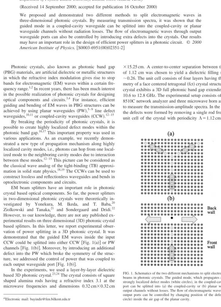
EM beam splitters have an important role in photonic crystal based optical components. So far, the power splitters in two-dimensional photonic crystals were theoretically in-vestigated by Yonekura, M. Ikeda, and T. Baba,20 Ziolkowski and Tanaka,21 and Sondergaard and Dridi.22 However, to our knowledge, there are not any published ex-perimental results on three dimensional共3D兲 photonic crystal based splitters. In this letter, we report experimental obser-vation of power splitting in a 3D photonic crystal. It was demonstrated that the guided EM waves inside the input CCW could be splitted into either CCW 关Fig. 1共a兲兴 or PW channels关Fig. 1共b兲兴. Moreover, by introducing an additional defect into the PW which broke the symmetry of the struc-ture, we addressed the control of power that was coupled to each output waveguide port关Fig. 1共b兲兴.
In the experiments, we used a layer-by-layer dielectric based 3D photonic crystal.23,24The crystal consists of square shaped alumina rods having a refractive index 3.1 at the microwave frequencies and dimensions 0.32 cm⫻0.32 cm
⫻15.25 cm. A center-to-center separation between the rods of 1.12 cm was chosen to yield a dielectric filling ratio of ⬃0.26. The unit cell consists of four layers having the sym-metry of a face centered tetragonal共fct兲 crystal structure. The crystal exhibits a 3D full photonic band gap extending from 10.6 to 12.8 GHz. The experimental setup consists of an HP 8510C network analyzer and three microwave horn antennas to measure the transmission-amplitude spectra. In the CCWs, the defects were formed by removing a single rod from each unit cell of the crystal with periodicity ⌳⫽1.12 cm.12 The
a兲Electronic mail: [email protected]
FIG. 1. Schematics of the two different mechanisms to split electromagnetic beams in photonic crystals. The guided mode, which propagates along the strongly localized defect modes共white circles兲, in the coupled-cavity input port can be splitted into 共a兲 the coupled-cavity or 共b兲 planar waveguide output channels without losses. The flow of electromagnetic waves through output ports can be controlled by changing position of the defect 共black circle兲 inside the air gap of the planar cavity.
APPLIED PHYSICS LETTERS VOLUME 77, NUMBER 24 11 DECEMBER 2000
3902
0003-6951/2000/77(24)/3902/3/$17.00 © 2000 American Institute of Physics
electric field polarization vector of the incident EM field was parallel to the rods of the defect lines for all measurements. In the TB approximation, two requirements must be sat-isfied simultaneously:19 共1兲 strong localization of the indi-vidual defect modes, 共2兲 weak interaction between these lo-calized modes. Under these conditions, photons can move along the defect sites in photonic crystals irrespective of the change in the direction of propagation. As an example, we have recently demonstrated that even if cavities were chosen to form a random path, nearly a full transmission could be achieved throughout the defect band.13 The CCWs can also be used to split EM waves in photonic band gap materials. We tested this power splitting argument by measuring the transmission spectra of two different splitter structures 共see Fig. 1兲.
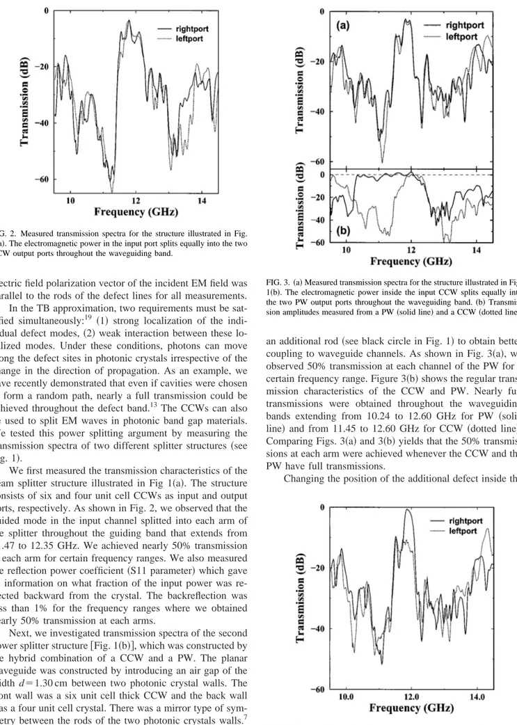
We first measured the transmission characteristics of the beam splitter structure illustrated in Fig 1共a兲. The structure consists of six and four unit cell CCWs as input and output ports, respectively. As shown in Fig. 2, we observed that the guided mode in the input channel splitted into each arm of the splitter throughout the guiding band that extends from 11.47 to 12.35 GHz. We achieved nearly 50% transmission at each arm for certain frequency ranges. We also measured the reflection power coefficient 共S11 parameter兲 which gave us information on what fraction of the input power was re-flected backward from the crystal. The backreflection was less than 1% for the frequency ranges where we obtained nearly 50% transmission at each arms.
Next, we investigated transmission spectra of the second power splitter structure关Fig. 1共b兲兴, which was constructed by the hybrid combination of a CCW and a PW. The planar waveguide was constructed by introducing an air gap of the width d⫽1.30 cm between two photonic crystal walls. The front wall was a six unit cell thick CCW and the back wall was a four unit cell crystal. There was a mirror type of sym-metry between the rods of the two photonic crystals walls.7 In this case, the EM waves inside the input CCW were di-vided into two parts throughout the guiding band and propa-gated along the two opposite arms of the PW. We also used
an additional rod共see black circle in Fig. 1兲 to obtain better coupling to waveguide channels. As shown in Fig. 3共a兲, we observed 50% transmission at each channel of the PW for a certain frequency range. Figure 3共b兲 shows the regular trans-mission characteristics of the CCW and PW. Nearly full transmissions were obtained throughout the waveguiding bands extending from 10.24 to 12.60 GHz for PW 共solid line兲 and from 11.45 to 12.60 GHz for CCW 共dotted line兲. Comparing Figs. 3共a兲 and 3共b兲 yields that the 50% transmis-sions at each arm were achieved whenever the CCW and the PW have full transmissions.
Changing the position of the additional defect inside the
FIG. 4. Transmission amplitude as a function of frequency for the switching structure. Changing the position of the extra defect关black circle in the Fig. 1共b兲兴, the powers in the right and left ports became around 90% and 6%, respectively.
FIG. 2. Measured transmission spectra for the structure illustrated in Fig. 1共a兲. The electromagnetic power in the input port splits equally into the two CCW output ports throughout the waveguiding band.
FIG. 3.共a兲 Measured transmission spectra for the structure illustrated in Fig. 1共b兲. The electromagnetic power inside the input CCW splits equally into the two PW output ports throughout the waveguiding band.共b兲 Transmis-sion amplitudes measured from a PW共solid line兲 and a CCW 共dotted line兲. 3903
Appl. Phys. Lett., Vol. 77, No. 24, 11 December 2000 Bayindir, Temelkuran, and Ozbay
PW section breaks the symmetry of the structure. This can be used to regulate the amount of power flow into the output ports. The structure can then be used as a switch by changing the position of the additional defect.21 To demonstrate the switching effect, we shifted the rod towards the left arm by 1 cm with respect to the center of the PW, and then measured the output power in each port. As shown in Fig. 4, this con-figuration drastically changed the output power in each port. While 90% of the input power was coupled to the right port, only 6% of the input power was coupled to the left port.
In conclusion, we have experimentally demonstrated photonic crystal based power splitters in which the input EM power can be efficiently divided into the output waveguide ports. Since Maxwell’s equations have no fundamental length scale, the results presented in this letter can be ob-served at optical wavelengths. Our structures can be used to construct power splitters in optical components and circuits. This work was supported by NATO Grant No. SfP971970, National Science Foundation Grant Nos. INT-9820646, Turkish Department of Defense Grant Nos. KOBRA-001 and Thales JP8.04.
1J. D. Joannopoulos, R. D. Meade, and J. N. Winn, Photonic Crystals:
Molding the Flow of Light共Princeton University Press, Princeton, NJ,
1995兲. 2
For a recent review, see articles in Photonic Band Gap Materials, edited by C. M. Soukoulis共Kluwer, Dordrecht, 1996兲.
3H. Kosaka, T. Kawashima, A. Tomita, M. Notomi, T. Tamamura, T. Sato, and S. Kawakami, Appl. Phys. Lett. 74, 1370共1999兲.
4
A. de Lustrac, F. Gadot, S. Cabaret, J.-M. Lourtioz, T. Brillat, A. Priou, and E. Akmansoy, Appl. Phys. Lett. 75, 1625共1999兲.
5A. Mekis, J. C. Chen, I. Kurland, Shanhui Fan, Pierre R. Villeneuve, and J. D. Joannopoulos, Phys. Rev. Lett. 77, 3787共1996兲.
6S.-Y. Lin, E. Chow, V. Hietala, P. R. Villeneuve, and J. D. Joannopoulos, Science 282, 274共1998兲.
7B. Temelkuran and E. Ozbay, Appl. Phys. Lett. 74, 486共1999兲. 8
T. Baba, N. Fukaya, and J. Yonekura, Electron. Lett. 35, 654共1999兲. 9M. Tokushima, H. Kosaka, A. Tomita, and H. Yamada, Appl. Phys. Lett.
76, 952共2000兲.
10M. M. Sigalas, R. Biswas, K. M. Ho, C. M. Soukoulis, D. Turner, B. Vasiliu, S. C. Kothari, and S. Lin, Microwave Opt. Technol. Lett. 23, 56 共1999兲.
11
A. Chutinan and S. Noda, Appl. Phys. Lett. 75, 3739共1999兲; S. Noda, K. Tomoda, N. Yamamoto, and A. Chutinan, Science 289, 604共2000兲. 12
M. Bayindir, B. Temelkuran, and E. Ozbay, Phys. Rev. Lett. 84, 2140 共2000兲.
13
M. Bayindir, B. Temelkuran, and E. Ozbay, Phys. Rev. B 61, R11855 共2000兲.
14
M. Bayindir and E. Ozbay, Phys. Rev. B 62, R2247共2000兲. 15M. Bayindir, S. Tanriseven, and E. Ozbay, Appl. Phys. A共in press兲. 16
E. Yablonovitch, T. J. Gmitter, R. D. Meade, A. M. Rappe, K. D. Brom-mer, and J. D. Joannopoulos, Phys. Rev. Lett. 67, 3380共1991兲. 17
E. Ozbay, G. Tuttle, M. M. Sigalas, C. M. Soukoulis, and K. M. Ho, Phys. Rev. B 51, 13961共1995兲.
18
N. Stefanou and A. Modinos, Phys. Rev. B 57, 12127共1998兲; C. Martijn de Sterke, Phys. Rev. E 57, 3502共1998兲; E. Lidorikis, M. M. Sigalas, E. N. Economou, and C. M. Soukoulis, Phys. Rev. Lett. 81, 1405共1998兲; A. Yariv, Y. Xu, R. K. Lee, and A. Scherer, Opt. Lett. 24, 711共1999兲. 19N. W. Ashcroft and N. D. Mermin, Solid State Physics共Saunders,
Phila-delphia, 1976兲, p. 175.
20J. Yonekura, M. Ikeda, and T. Baba, J. Lightwave Technol. 17, 1500
共1999兲.
21R. W. Ziolkowski and M. Tanaka, Opt. Quantum Electron. 31, 843
共1999兲.
22
T. Sondergaard and K. H. Dridi, Phys. Rev. B 61, 15688共2000兲. 23K. M. Ho, C. T. Chan, C. M. Soukoulis, R. Biswas, and M. M. Sigalas,
Solid State Commun. 89, 413共1994兲. 24
E. Ozbay, J. Opt. Soc. Am. B 13, 1945共1996兲.
3904 Appl. Phys. Lett., Vol. 77, No. 24, 11 December 2000 Bayindir, Temelkuran, and Ozbay