ARAŞTIRMA MAKALESİ (Research Article)
108
THE STRUCTURAL, SURFACE MORPHOLOGY, OPTICAL AND ELECTRICAL PROPERTIES OF ZnO FILM DOPED GALLIUM AT 10%
Senem AYDOĞU1, Seda UZKALAN2 1 Kütahya Dumlupınar University, Department of Physics, Faculty of Art and Science, Kütahya,
[email protected], ORCID: 0000-0003-2426-9162
2 Kütahya Dumlupınar University, Department of Physics, Faculty of Art and Science, Kütahya, [email protected];
ORCID: 0000-0003-2564-6484
Geliş Tarihi: 30.11.2018 Kabul Tarihi: 30.12.2019
ABSTRACT
The pure and 10% gallium (Ga) doped zinc oxide (ZnO) films synthesized on glass substrates by ultrasonic spray pyrolysis technique. The structural, surface morphology, optical and electrical properties of pure and doped films were analysed by X–ray diffraction (XRD) pattern, atomic force microscopy (AFM), Ultraviolet – Visible (UV–Vis) spectrophotometer and four probe technique, respectively. It observed from the results of XRD that the preferred orientation changed from (100) to (002) with Ga doping at 10 %. Also, the grain size and strain values of films calculated both Scherrer Method and Williamson–Hall (W–H) Method were compared. In the result of this comparison, the values calculated by Scherrer Method were found to be smaller than the values calculated by W–H Method. All experimental results show that the grain size, surface roughness, energy band gap and electrical conductivity increased as its Urbach energy decreased with the addition of gallium. As a result, the crystallinity of ZnO film was observed to improve with doping Ga at 10 %.
Keywords: Ultrasonic spray pyrolysis, Williamson–Hall Method, Optical properties, Urbach energy
%10 GALYUM KATKILI ZnO FİLMİNİN YAPISAL, YÜZEY MORFOLOJİSİ, OPTİK ve ELEKTRİK ÖZELLİKLERİ
ÖZ
Saf ve %10 galyum (Ga) katkılı çinko oksit (ZnO) filmlerinin ultrasonik sprey piroliz tekniğiyle cam tabanlar üzerine sentezlendi. Saf ve katkılı filmlerin yapısal, yüzey morfolojisi, optik ve elektriksel özellikleri X–ışını kırınım (XRD) örneği, atomik kuvvet mikroskopisi (AFM), ultraviyole ve görünür ışık (UV–Vis) spektrofotometresi ve dört prob tekniği ile analizlendi; sırasıyla. XRD sonuçlarından %10 Ga katkılanmasıyla tercihli yönelimin (100) dan (002) ye değiştiği gözlendi. Ayrıca, hem Scherrer Metodu hem de Williamson–Hall (W–H) Metodu ile hesaplanan filmlerin tanecik boyutu ve gerilim değerleri karşılaştırıldı. Bu karşılaştırmanın sonucunda, Scherrer Metoduyla hesaplanan değerler W–H Metodu ile hesaplanan değerlerden daha küçük bulundu. Tüm deneysel sonuçları,
109
galyum katkısıyla Urbach enerjisi azalırken, tanecik boyutunun, yüzey pürüzlülüğünün, enerji band aralığının ve elektrik iletkenliğinin arttığını göstermiştir. Sonuç olarak, ZnO filminin kristalliği %10 Ga katkısıyla geliştiği gözlenmiştir.
Anahtar Kelimeler: Ultrasonik sprey piroliz, Williamson – Hall Metodu, optik özellikler, Urbach enerjisi
1. INTRODUCTION
Zinc oxide (ZnO) is mainly used in many applications, including microelectronic and optoelectronic devices [1, 2, 3, 4]. The main reasons of ZnO preference are the optical properties and electrical conductivity, high thermal and chemical stability, non–toxicity and abundance in nature. Because of these properties, ZnO has attracted much attention in transparent conducting oxides (TCO). Generally ZnO, n type semiconductor in hexagonal structure, has a direct band transition energy gap 3.3 eV at room temperature[2, 5]. ZnO may be improved the structural, optical and electrical properties by doped III group elements (Ga, Al, In). Hence, doping of specific elements (Ga, In, Mg) leads to change in the band gap and so the activation energy of the donor centres and this causes their stability [1, 3, 6–11]. Doping ZnO with these metals has the properties of high transparency and low resistivity [12]. In recent years, the Ga, Al, Mg doped ZnO films have been observed to improve photocatalysis property and researches on this property of films have increased [13–17]. Among these even for doping high Ga has a good lattice matching with ZnO lattice and is less reactive with oxygen. Both ionic and covalent radii of gallium (0.62Å, 1.26Å) are closed to that of ZnO (0.74Å, 1.31Å)[18].This makes the gallium one of the best dopant and causes minimal lattice distortion.
ZnO and ZnO:Ga thin films can be produced by different methods: Molecular beam epitaxy (MBE) [19], magnetron sputtering [7,20], chemical vapour deposition (CVD) [21,22], pulsed laser deposition (PLD) [23,24], chemical spray pyrolysis [2, 5, 25], sol–gel [26, 27]. The chemical spray pyrolysis technique was first used by Chamberlin and Skarman [28] in 1966 to produce CdS and some inorganic sulphide and selenite thin films. In the following years, this technique has been developed and used to deposition a wide variety of films. In this technique thin film can be produced to the desired properties by adjusting the experimental parameters. In the last 20 years three spray pyrolysis techniques have been developed with different atomization techniques [29,30]: Preumatic [31,32], Ultrasonic [31,33] and Electrostatic spray pyrolysis [31,34,35] techniques (PSP, USP, ESP respectively). USP technique is a technique based on spraying aqueous solution prepared in a particular the concentrations and volumes of salt containing the elements of obtained materials on preheated glass, metallic or ceramic substrates in a certain flow rate using a certain time the carrier gas as nitrogen gas or air [36,37]. USP has a number of advantages such as simple and economically contains cheap tools, ensuring as soon as materials production, low energy consumption, simply different atoms doped, the ability deposited film on a large surface and not require vacuum. The films obtained by spray pyrolysis technique have a polycrystalline structure [36,37].
A perfect crystal expands periodically in all directions to infinity. However no crystals are ideal, so it is not perfect. The broadening of the diffraction peaks is the result of the deflection from perfect crystallinity. Peak width analysis gives the information about crystal size and strain. The particle size does not generally mean the same as the crystallite (grain) size of the particles. Because the presence of polycrystalline aggregates in the film structure is mentioned. A measure of the distribution of lattice constants caused by crystal defects is the lattice strain [38]. The investigation of dislocation distribution is done using X–ray line broadening. The X–ray diffraction analysis is used to predict the
110
crystallite size and lattice strain [39,40]. There are available methods to predict the crystallite and lattice tension [38,41]. One generally used analysis is Williamson Hall (W–H) analysis. This analysis is an alternative method for computing the crystallite size and lattice strain [38,39,41]. Uniform deformation model (UDM), uniform deformation stress model (UDSM) and uniform deformation energy density model (UDEDM) are the changed forms of W–H analysis [42].
In the literature research, Ga doped ZnO films were produced with different techniques. Ga additive ratios were generally in the range of 1 - 9% and films were obtained [12,42–50]. In these studies, structural, optical, electrical properties of films were investigated. In addition, ZnO films were not doped with 10% gallium and were not examined by W - H theory. The first aim of this work is that the ZnO and ZnO:Ga (10 %) films produced by USP on the glass substrates are examined the structural, surface morphology, optical and electrical properties. A perfect crystal would extend infinitely in all directions. Therefore, crystals are no perfect because of their finite size. The broadening of the diffraction peaks is the cause of the deviation from perfect crystallinity. The grain size and lattice strain are obtained from peak width analysis and affect the Bragg peak in different ways. The grain size of the particle is not the same as the particle size because of the formation of polycrystalline aggregates. While reviewing the literature, there are no works considering this broadening. Therefore broadening must be taken into account to calculating the crystallite (grain) sizes and other aim of this work is that the examining of the crystal structures of films is done with Scherrer method and W–H analysis, and the results calculated with each method are compared. Furthermore, UDM approach in the W–H analysis is used. In UDM, the crystal is considered having the isotropic nature. In addition, the energy band gaps and Urbach energies of the films were calculated as a result of examining the optical properties.
2. EXPERIMENTAL DETAILS
The films of pure and ZnO doped Ga at 10% were deposited by USP technique. Zn(CH3COO)2.2H2O and GaN3O9.xH2O were utilized the precursor aqueous solutions as ZnO and Ga sources, respectively. The dopant concentration (Ga at %) was measured 10 % as volume percentage. The precursor solutions were sprayed onto the heated glass substrates at a constant temperature of 380°C±5°C. Substrate was heated by quartz heater. The experimental parameters are tabulated in Table 1.
Table 1. The experimental parameters used to produce the films.
Material ZnO, ZnO:Ga
Dopind level (at %) 10
Source Solutions Zn(CH3COO)2.2H2O and GaN3O9.xH2O
Molarity 0.1M
Total volume of spraying solution 100ml.
Substrate temperature 380±5°C
Solution flowrate 5 ml/min
Spraying time 20 min
Nozzle to substrate distance 27cm
Carrier gas / pressure Air / 2 bar
The crystal structures of the films were obtained by Bruker D8 – X – Ray Diffractometer using CuKα radiation of λ=1.5406Å in the detector scan mode in the range of 20°–75°. The absorbance, transmittance and optical band gap of films were investigated by Shimadzu UV–Vis 1800
111
spectrophotometer covering the spectral range from 190 – 1100nm. The surface morphologies were scanned in area of 2 m2 m using Park System XE–100 Atomic Force Microscope (AFM) in non– contact mode. XEI version 1.7.1 software is used for obtaining root mean square (rms, Rq), average (Ra) and peak to valley (Rqv) roughness values. The electrical properties of films were searched by four probe technique with Pro4 Lucas Keithley 2601A System Sourcemeter.
3. RESULTS AND DISCUSSIONS
3.1. XRD Analysis
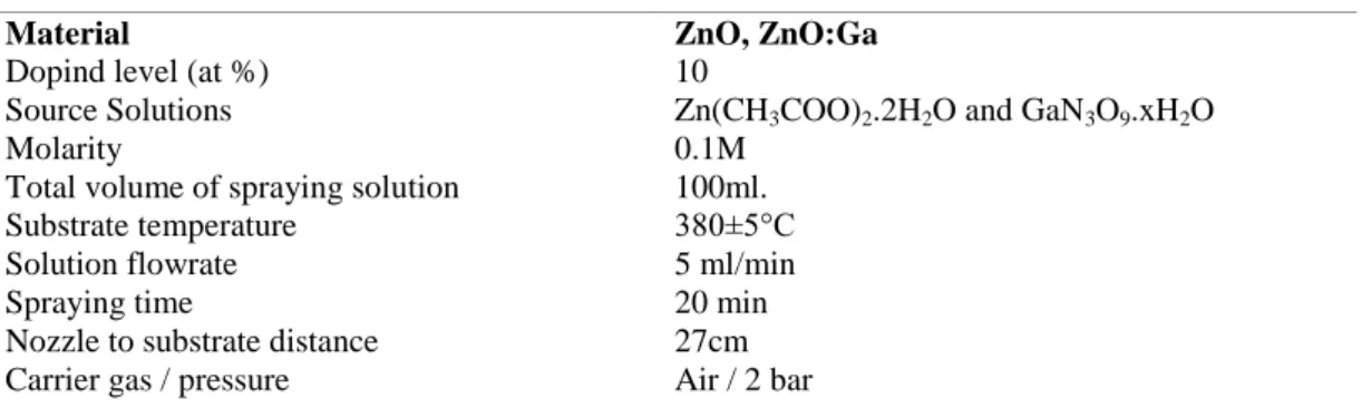
The structural properties of the ZnO and ZnO:Ga (10 %) films have been determined from X–ray diffraction technique using CuKα (1.5406Å) as given in Figure 1. The main peaks for pure ZnO film in Figure 1(a) were observed the planes of (100), (002), (101), (110); not too prominent peaks were (102), (103), (200), (112) and (201). It is seen in Figure 1(b) that the peaks of (100), (002), and (101) were permanent peaks as intensity of (110) peak was reduced. Fig.1 indicates that both pure and Ga doped ZnO films has the polycrystalline nature correspond to hexagonal structure ZnO powder (PDF 01–070–8070; PDF: powder diffraction file). There is an intense peak which belong to the reflections from (100) in Figure 1(a) and from (002) plane of ZnO:Ga in Figure 1(b). Accordingly, it is observed that the preferred orientation from (100) to (002) was changed with the Ga doping at 10%. In Fig. 1(b) there was no peak of another phase such as gallium. Also, because the films are produced on glass substrates, the amorphous structure of the glass is observed in XRD pattern. Therefore, a decrease between 38° and 46° is observed.
112
(b)Figure 1. XRD patterns for (a) ZnO and (b) ZnO:Ga.
The lattice constants (a = b, c) of undoped and doped films are calculated from below equation using interplanar spacing of different (hkl) planes,
1 dhkl2
=
4 3(
h2+hk+k2 a2) +
l2 c2 (1)where (hkl) are the Miller indices; a, b, c are the lattice constants and dhkl is the interplanar spacing. The lattice constant values of pure sample for (100) direction plane are slightly bigger than the value of the corresponding standard material (PDF Card No: 01–070–8070). The reason of this difference may be due to healing of the material. Because the oxygen vacancies can be filled by the Ga atoms and the interstitial Ga atoms, leading to an increase in the lattice strain. The lattice constant values of the films obtained from Eq. 1 and lattice constants of the corresponding standard material are given in Table 2.
Table 2. The lattice constants of ZnO and ZnO:Ga films.
Lattice Constants ZnO (100) ZnO:Ga (10%) (002) PDF Card 01–070–8070 a (Å) 3.6016 3.2504 3.24890 b (Å) 3.6016 3.2504 3.24890 c (Å) c/a 5.7844 1.6061 5.2073 1.6021 5.20490 1.6021
113
In the literature [11,18], as ZnO doped Ga at 1–7 % concentration, it seen that there was no structural change or Ga2O3 phase was not occurred. Bartina et al. [10] examined that the optical and electrical properties of Al, Ga and In with 0–10 % doped ZnO films and saw that the structure of ZnO films no chanced. Also Sharma et al. [50] observed that the structures of ZnO films, produced by spin coating method and annealed, no changed with doping Ga at 11.05 %. Nakagawara et al. [51] examined to ZnO films with Ga heaving doping (4.3–23.1 %) and so, they observed that the peak in XRD pattern completely disappears in the 23.1 % Ga doped ZnO. Contrary to their works, it is observed in this work that the preferential growth of ZnO film was became from (100) to (002) plane with doping Ga at 10%. It is attributed to the crystal reorientation and so structural change is caused by the incorporation of further more Ga atoms. According to Barbar et al. [25] and Winer et al. [27], the crystallinity deterioration affects the crystal reorientation originating from addition of more Ga atom. Because the mechanical stress occur from differences in the ionic radii of Ga (0.062nm) and Zn (0.074nm), and so this may be degraded the crystallinity of film at higher doping concentration. 3.1.1. Scherrer Method and Williamson–Hall Method
A perfect crystal would extend infinitely in all directions. Therefore, crystals are no perfect because of their finite size. The broadening of the diffraction peaks is the cause of the deviation from perfect crystallinity. The grain size and lattice strain are obtained from peak width analysis and affect the Bragg peak in different ways. The grain size of the particle is not the same as the particle size because of the formation of polycrystalline aggregates [52]. The one of aims of the present work is to obtain the crystallite sizes and strains of produced films using both Scherrer Method and Williamson Hall Method (W–H).
The peak broadening occurred with grain size and lattice strain could be evaluating using XRD. The crystalline size (D) and the strain (
) were obtained using the Scherrer Method based on (100) plane for ZnO and based on (002) plane for Ga:ZnO [53]:D= 0.9λ βcosθ⁄ (2)
ε = βcosθ 4⁄ (3)
where D is the grain size, λ is the wavelength of the radiation, is the peak width at half maximum intensity (FWHM) and θ is Bragg angle. In semiconductors, the phonon-induced lattice vibrations, lattice mismatched film growth, and applied external stress creates the strain [54]. It is necessary to take into account the conduction energy band shift with strain; and there is strain effect. The length of dislocation lines per unit volume of crystal defines the dislocation density. Thus the defects in the films can be quantified. The dislocation density () was calculated from Eq. 4,
δ = 1 D⁄ 2 (4)
The sharp and narrow peaks in XRD pattern indicate good crystallization. This defines that the should be small. Thus, the small size of the ensures that the grain size is large, which defines good crystallization of the films. According to Eq. 4, larger D, smaller and smaller indicates that it is better crystallization of film [55]. The grain sizes (D), strains and dislocation density were calculated using the Scherer’s formula for the (100) line of pure ZnO and for the (002) line of ZnO:Ga. As also show in Table 3, the crystalline of ZnO film is improved with Ga doping.
114
Strain-induced broadening due to crystal imperfections and deformity are dependent on the tan θ in W–H analysis. The distinct θ dependencies of both grain size and strain effects provided a basis for the separate identification of both broadening in the W–H Theory:
βhkl= (0.9λ Dcosθ⁄ ) + (4εtanθ) (5)
βhklcosθ = (0.9λ D⁄ ) + (4εsinθ) (6)
Eqs. 5 and 6 represent UDM. According to this method, the nature of crystal is assumed mechanically isotropic. The properties of the material are isotropic depending on its crystallographic orientation.
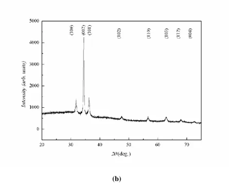
Figure 2. Plot of hkl.cosθ vs 4sinθ of ZnO film.
115
Table 3. The grain size (D), dislocation density () and strain () values of ZnO and ZnO:Ga films.
The plots of βhklcos θ vs 4 sin θ for all samples are drawn (Figs. 2–3). The strain and grain size can
estimate from the slope and y–intercept of βhklcos θ vs 4 sin θ plots, respectively. The values of D
and are calculated using Scherrer Method and W–H Analysis for ZnO and ZnO:Ga films and given in Table 3. Furthermore, the values of (hkl), 2θ and βhkl used for Scherrer Method and W–H Method
are summarized in Table 4.
Table 4. The values of βhkl, (hkl), 2θ and I used for Scherrer Method and W–H Method.
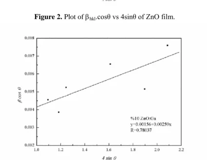
Material (hkl) 2θ 𝛃𝐡𝐤𝐥×10 – 3 (rad) PDF Card 01–070–8070
ZnO (100) 31.8142 6.374 31.778 (002) 34.284 7.1370 34.434 (101) 36.2188 8.4906 36.265 (110) 56.6672 9.8046 56.613 (112) 67.9051 12.116 67.971 ZnO:Ga (100) 31.7627 4.7409 31.778 (002) 34.4178 4.0409 34.434 (101) 36.2394 5.5134 36.265 (102) 47.5184 7.1565 47.556 (110) 56.5746 5.8598 56.613 (103) 62.8521 8.9065 62.880
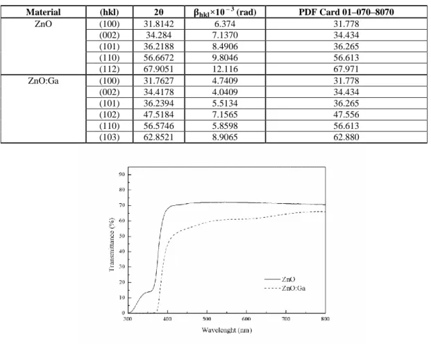
Figure 4. Transmission of ZnO and ZnO:Ga films. Sherrer Theory Williamson-Hall Theory Sample D (nm) 10–3 (nm)–2 ε10–4 D (nm) 10–3 (nm)–2 ε10–4 ZnO 20.445 2.392 15.3 38.092 6.892 15.5 ZnO:Ga 35.921 0.775 9.64 88.880 0.127 25.9
116
3.2. Optical PropertiesFig. 4 shows the transmission for undoped and Ga doped ZnO films. The average transparency of ZnO and ZnO:Ga films was seen around 70 % – 64 % towards high wavelengths, respectively (Fig. 4). The transmittance of the ZnO film could be reduced with Ga doping. The decreasing transmittance of Ga doped ZnO film is due to defects, light scattering and/or irregularities in the film structure[12].
(a)
(b)
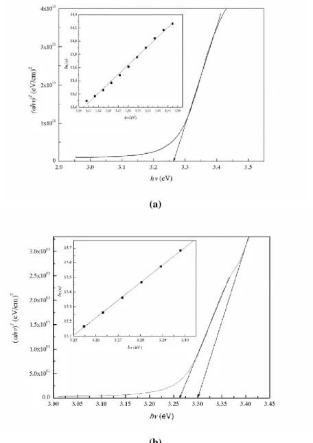
Figure 5. (αhν)2 versus hν for (a) ZnO and (b) ZnO:Ga films. Insets: Plots of ln (α) versus photon energy (h).
117
The optical absorption method is also used to determine the forbidden energy ranges of semiconductors as well as to determine band structures. A determined of the optical band gap can be also defined by a direct transition between the valance band and conduction band in the high absorption region. The following equation is used to obtain the optical band gap:
α = A(hγ − Eg)n (7)
where A is constant, h is Planck’s constant and ν is the frequency of the radiation. The most suitable value for n is obtained as ½ from the optical absorption method graphics. n = 1/2 indicates that transitions are direct band transitions. The optical band gap values of films were obtained with extrapolating from the appropriate absorption edge to (αhν)2=0 in Tauc’s plot. According to Fig. 5, pure and Ga doped ZnO films have the direct band gap and are 3.26 eV and 3.30 eV, respectively. But in Fig. 5(b) the first energy (Eg1) the second energy (Eg2) are seen, and are the forbidden energy gap of ZnO film and the transition energy to energy levels of impurities and defects formed with Ga incorporating, respectively. Addition to the semiconductor often reveals band tail formation in the band gap. This is defined as Urbach's energy, which indicates the possible optical transitions between unoccupied and occupied states. Therefore Urbach energy is calculated for ZnO and ZnO:Ga films. Urbach rule is expressed in Eqs. 8 and 9 in the exponential edge region 56;
α = αoexp[hγ E⁄ ] U (8)
EU= [dlnα dhγ⁄ ]−1 (9)
The value of Urbach energy (EU) obtained from the inverse of the slope of graph at Fig. 5 (insets). The width of the localized states in the optical band gap could be change with doping. The optical band gap varies inversely with the EU values 46. The Urbach energy was decreased with Ga doping from 180 to 89 meV and the optical band gap value was increased with Ga doping from 3.26 to 3.30 eV. The observed decrease in the Urbach energy values and increase in the optical band gap with Ga doping can be defined by the decrease in lattice defects. This is consistent with the results of XRD analysis. That is, it corresponds to increased crystallites and peak intensities and reduction of dislocation defects. So, these results are consisted with the literature 57,58.
3.3. Surface Morphology
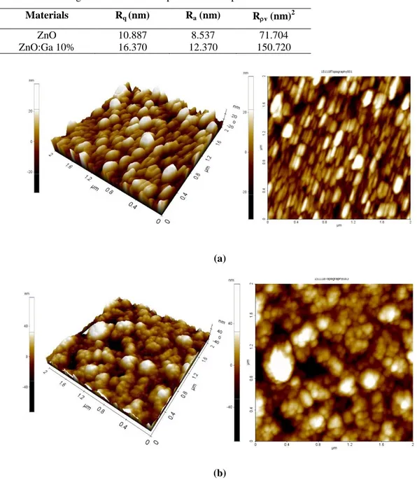
The surface morphology of thin films varies with the experiment technique and the experimental parameters. The mechanical, electrical and optical properties of thin films affect by the surface morphology. The development of electrical conductivity and optical transmittance can be achieved by decreasing grain boundary and active surface expansion [59]. With this aim, the surface morphology of produced films was investigated with AFM.
The AFM images of the pure and ZnO:Ga (10 %) in both 2D and 3D forms are shown in Fig. 6. The ZnO film exhibits spherical formed grain with granular morphology in Fig. 6(a). The ZnO film doped Ga at 10% indicates polycrystalline nature with voids free surface area and smaller spherical shaped particles in Fig. 6(b), also in the morphology of this film the larger sized grains are observed with the voids and cracks.
118
Table 5. The roughness values for the pure and Ga doped ZnO films. Materials Rq (nm) Ra (nm) Rv (nm)2
ZnO 10.887 8.537 71.704
ZnO:Ga 10% 16.370 12.370 150.720
(a)
(b)
119
3.4. Electrical PropertiesThe resistivity of pure and Ga doped ZnO films were measured by four probe method. Electrical resistivity values of ZnO and ZnO:Ga are obtained as 3.47104 Ωm and 19.76 Ωm, respectively. It is seen that the electrical conductivity of pure film was increased with Ga doping.
In the literature study 11,60, it was observed that the grain size decreased and the surface roughness decreased with the addition of gallium to the ZnO films produced by the sol-gel technique. It is stated that in the heavily doped films, the degraded film crystallinity or segregation of dopant at the grain boundaries increase the electrical resistivity. In this work, the increase in the grain size and roughness of the ZnO film with the addition of gallium also resulted in an increase in the electrical conductivity. The reason for this is that the increase in the grain size can probably cause a decrease in grain boundary, related barriers and the surface states. This can reduce the capture traps of carriers and the ability of scattering, hence resulting in a lower resistivity and so a higher conductivity. This is supported by the results of XRD, AFM and four probe measurements. It is also convenient with the literature 42.
4. CONCLUSION
ZnO and ZnO:Ga (10%) are synthesized using USP technique. The structural, optical, morphological and electrical properties of films were searched with XRD, UV–VIS, AFM and four probe methods. From XRD patterns it seen that the orientation of ZnO film is changed from (100) to (002) plane and the crystalline size increased with Ga doping. The grain sizes of films obtained from Scherrer Method were smaller than the grain sizes obtained from W–H Analysis. This difference is proportional to the strain value and indicates that the strain plays an important role. Therefore instrument broadening must be taken into account to calculating the grain size. In addition to this reorientation, the optical band gap of pure ZnO increased with Ga doping. Compared to ZnO film, Ga doped ZnO film has the changed structural, large grain size, large band gap value, high electrical conductivity. In this study, the observed decreased in electrical resistivity at 10 % Ga doped ZnO film originate from improvement in the crystallinity and increase in grain sizes with decreasing in grain boundaries. According to these results the crystallinity of ZnO film can be improved with doped Ga. The gallium-doped ZnO film (10%) produced by spray pyrolysis technique can be used for gas sensors due to its large surface area, high surface roughness and high conductivity.
ACKNOWLEDGEMENTS
Project supported by Kutahya Dumlupınar University Commision of Scientific Research Projects grant number 2015–3. Authors would like to thank Assoc. Prof. A. Şenol Aybek for XRD spectra measurements and Prof. Dr. Ferhunde Atay and Prof. Dr. İdris Akyüz for AFM measurements.
REFERENCES
[1] Kumar, M., Singh, B., Yadav, P., Bhatt, V., Kumar, M., Singh, K., Abhyankar, A. C., Kumar, A. and Yun, J. H., (2017), Effect of structural defects, surface roughness on sensing properties of Al doped ZnO thin films deposited by chemical spray pyrolysis technique, Ceram. Int. 43, 3562– 3568.
120
[2] Manoharan, C., Dhanapandian, S., Arunachalam, A. and Bououdina, M., (2016), Physical properties of spray pyrolysized nano flower ZnO thin films, J. Alloy. Comp., 685, 395–401. [3] Demchenko, D. O., Earles, B., Liu, H. Y., Avrutin, V., Izyumskaya, N., Ozgur, U. and Morkoc,
H., (2011), Impurity complexes and conductivity of Ga-doped ZnO, Phys. Rev. B: Condens. Matter., 84, 075201–5.
[4] Enigochitra, A. S., Perumal, P., Sanjeeviraja, C., Deivamani, D. and Boomashri, M., (2016), Influence of substrate temperature on structural and optical properties of ZnO thin films prepared by cost–effective chemical spray pyrolysis technique, Superlattices Microstruct., 90, 313–320. [5] Muchuweni, E., Sathiaraj, T. S. and Nyakotyo, H., (2016), Effect of gallium doping on the
structural, optical and electrical properties of zinc oxide thin films prepared by spray pyrolysis, Ceram. Int., 42, 10066–10070.
[6] Gabas, M., Landa–Canovas, A., Costa–Kramer, J. L., Agullo–Rueda, F., Gonzalez–Elipe, A. R., Diaz–Carrasco, P., Hernandez–Moro, J., Lorite, I., Herrero, P., Castillero, P., Barranco, A. and Ramos–Barrado, J. R., (2013), Differences in n–type doping efficiency between Al– and Ga– ZnO films, J. Appl. Phys., 113, 163709–9.
[7] Jia, J., Yoshimura, A., Kagoya, Y., Oka, N. and Shigesato, Y., (2014), Transparent conductive Al and Ga doped ZnO films deposited using off-axis sputtering, Thin Solid Films, 559, 69–77. [8] Olvera, M de la L., Gomez, H. and Maldonado, A., (2007), Doping, vacuum annealing, and
thickness effect on the physical properties of zinc oxide films deposited by spray pyrolysis, Sol. Energy Materials Sol. Cells, 91, 1449–1453.
[9] Oh, S. J., Jung, M. N., Ha, S. Y., Choi, S. G., Kim, J. J., Kobayashi, K., Lee, S. T., Lee, H. C., Cho, Y. R., Yao, T. and Chang, J. H., (2008), Microstructure evolution of highly Ga–doped ZnO nanocrystals, Physica E, 41, 31– 35.
[10] Barnita, P., Budhi, S., Subhasis, G. and Anushree, R., (2016), A comparative study on electrical and optical properties of group III (Al, Ga, In) doped ZnO, Thin Solid Films, 603, 21–28. [11] Tsay, C. Y., Wu, C. W., Lei, C. M., Chen, F. S. and Lin, C. K., (2010), Microstructural and
optical properties of Ga–doped ZnO semiconductor thin films prepared by sol–gel process, Thin Solid Films, 519, 1516–1520.
[12] Ivanova, T., Harizanova, A., Koutzarova, T. and Vetruyen, B., (2017), Optical and structural study of Ga and In co-doped ZnO films, Colloids Surf. A., 532, 357–362.
[13] Li, C. and Hou, Q., (2020), Built-in magnetic-electrical coupling enhances photocatalytic performance of GaN/ZnO: A first principle study, Physica B., 579, 411902–411905.
[14] Li, X., Hu, Z., Liu, J., Li, D., Zhang, X., Chen, J. and Fang, J., (2016), Ga doped ZnO photonic crystals with enhanced photocatalytic activity and its reaction mechanism, Applied Catalysis B: Environmental, 195, 29–38.
121
[15] Ali, A., Zhao, X., Ali, A., Duan, L., Niu, H., Peng, C., Wang, Y. and Hou, S., (2015), Enhanced photocatalytic activity of ZnO nanorods grown on Ga doped seed layer, Superlattices and Microstructures, 83, 422–430.
[16] Sitthichai, S., Phuruangrat, A., Thongtem, T. and Thongtem, S., (2017), Influence of Mg dopant on photocatalytic properties of Mg–doped ZnO nanoparticles prepared by sol–gel method, Journal of the Ceramic Society of Japan, 125(3), 122–124.
[17] Dhawan, R. and Panda, E., (2019), Mg addition in undoped and Al–doped ZnO films: Fabricating near UV transparent conductor by bandgap engineering, Journal of Alloys and Compounds, 788, 1037–1047.
[18] Moditswe, C., Muiva, C. M. and Juma, A., (2016), Highly conductive and transparent Ga–doped ZnO thin films deposited by chemical spray pyrolysis, Optik, 127, 8317–8325.
[19] Mandalapu, L. J., Xiu, F. X., Yang, Z. and Liu, J. L., (2007), Ultraviolet photoconductive detectors based on Ga–doped ZnO films grown by molecular beam epitaxy, Solid–State Electron., 51, 1014–1017.
[20] Young, S. J. and Liu, Y. H., (2015), Ultraviolet photodetectors with Ga–doped ZnO nanosheets structure, Microelectron. Eng., 148, 14–16.
[21] Kaul, A. R., Gorbenko, O. Yu., Botev, A. N. and Burova, L. I., (2005), MOCVD of pure and Ga doped epitaxial ZnO, Superlattices Microstruct. 38, 272–282.
[22] Terasako, T., Ogura, Y., Fujimoto, S., Song, H., Makino, H., Yagi, M., Shirakata, S. and Yamamoto, T., (2013), Carrier transport and photoluminescence properties of Ga–doped ZnO films grown by ion–plating and by atmospheric–pressure CVD, Thin Solid Films, 549, 12–17. [23] Berry, J. J., Ginley, D. S. and Burrows, P. E., (2008), Organic light emitting diodes using a
Ga:ZnO anode, Appl. Phys. Lett. 92, 193304–3.
[24] Estrada, M., Rivas, M., Garduño, I., Avila Herrera, F., Cerdeira, A., Pavanello, M., Mejia, I. and Quevedo Lopez, M. A., (2016), Temperature dependence of the electrical characteristics up to 370 K of amorphous In–Ga–ZnO thin film transistors, Microelectronics Reliability, 56, 29–33. [25] Babar, A. R., Deshamukh, P. R., Deokate, R. J., Haranath, D., Bhosale, C. H. and Rajpure, K. Y.,
(2008), Gallium doping in transparent conductive ZnO thin films prepared by chemical spray pyrolysis, J. Phys. D: Appl. Phys., 41, 135404–6.
[26] Tang, W. and Cameron, D. C., (1994), Aluminum–doped zinc oxide transparent conductors deposited by the sol–gel process, Thin Solid Films, 238, 83–87.
[27] Winer, I., Shter, G. E., Mann Lahav, M. and Grader, G. S., (2011), Effect of solvents and stabilizers on sol–gel deposition of Ga–doped zinc oxide TCO films, J. Mater. Res. 26(10), 1309–1315.
[28] Chamberlin, R. R. and Skarman, J. S., (1966), Chemical Spray Deposition Process for Inorganic Films, Technical Notes, 113(1), 86–89.
122
[29] Patil, P. S., (1999), Versatility of chemical spray pyrolysis technique, Materials Chemistry and Physics, 59, 185–198.
[30] Untila, G.G., Kost, T.N. and Chebotareva, A.B., (2019), Fluorine–doped ZnO (FZO) films produced by corona–discharge–assisted ultrasonic spray pyrolysis and hydrogenation as electron–selective contacts in FZO/SiOx/p–Si heterojunction crystalline silicon solar cells with 11.7% efficiency, Solar Energy, 179, 352–362.
[31] Untila, G.G., Kost, T.N. and Chebotareva, A.B., (2019), F–In–codoped ZnO (FIZO) films produced by corona–discharge–assisted ultrasonic spray pyrolysis and hydrogenation as electron–selective contacts in FIZO/SiOx/p–Si heterojunction crystalline silicon solar cells with 10.5% efficiency, Solar Energy, 181, 148–160.
[32] El Hichou, A., Addou, M., Mansori, M. and Ebothe J., (2009), Structural, optical and luminescent characteristics of sprayed fluorine–doped In2O3 thin films for solar cells, Solar Energy Materials & Solar Cells, 93, 609–612.
[33] Zhou, Z.B., Cui, R.Q., Pang, Q.J., Wang, Y.D., Meng, F.Y., Sun, T.T., Ding, Z.M. and Yu, X.B., (2001), Preparation of indium tin oxide films and doped tin oxide films by an ultrasonic spray CVD process, Applied Surface Science, 172, 245–252.
[34] Abbas, T. A–H., Slewa, L. H., Khizir, H. A. and Kakil, S. A., (2017), Synthesis of cobalt oxide (Co3O4) thin films by electrostatic spray pyrolysis technique (ESP), J. Mater. Sci.: Mater. Electron., 28(2), 1951–1957.
[35] Siefert, W., (1984), Corona Spray Pyrolysis: A new coating technique with an extremely enhanced deposition efficiency, Thin Solid Films, 120, 261–214.
[36] Kul, M., Aybek, A. S., Turan, E., Zor, M. and Irmak, S., (2007), Effects of fluorine doping on the structural properties of the CdO films deposited by ultrasonic spray pyrolysis, Solar Energy Materials & Solar Cells, 91, 1927–1933.
[37] Kul, M., Zor, M., Aybek, A. S., Irmak, S. and Turan, E., (2007), Electrical and optical properties of fluorine doped CdO films deposited by ultrasonic spray pyrolysis, Sol. Energy Mater. Sol. Cells, 91, 882–887.
[38] Khorsand Zak, A., Majid, W. H. A., Abrishami, M. E. and Yousefi, R., (2011), X–ray analysis of ZnO nanoparticles by Williamson Hall and size strain plot methods, Solid State Sciences, 13, 251–256.
[39] Mote, V. D., Purushotham, Y. and Dole, B. N., (2012), Williamson-Hall analysis in estimation of lattice strain in nanometer-sized ZnO particles, Journal of Theoretical and Applied Physics, 6(6), 2–8.
[40] Monshi, A., Foroughi, M. R. and Monshi, M. R., (2012), Modified Scherrer equation to estimate more accurately nano–crystallite size using XRD, Word Journal of Nano Science and Enginnering, 2, 154–160.
123
[41] Jeyaprakash, B. G., Kesavan, K., Ashok Kumar, R., Mohan, S. and Amalarani, A., (2011), Temperature dependent grain-size and microstrain of CdO thin films prepared by spray pyrolysis method, Bull. Mater. Sci. 34(4), 601–605.
[42] Chaabouni, F., Khalfallah, B. and Abaab, M., (2016), Doping Ga effect on ZnO radio frequency sputtered films from a powder target, Thin Solid Films, 617, 95–102.
[43] Chen, Y., Meng, F., Ge, F. and Huang, F., (2017), Ga-doped ZnO films by magnetron sputtering at ultralow dischargevoltages: Effects of defect annihilation, Thin Solid Films, 644, 16–22. [44] Cheng, H., Deng, H., Wang, Y. and Wei, M., (2017), Influence of ZnO buffer layer on the
electrical, optical and surface properties of Ga–doped ZnO films, Journal of Alloys and Compounds, 705, 598–601.
[45] Gabás, M., Ochoa–Martínez, E., Navarrete–Astorga E., Landa–Cánovas, A.R., Herrero, P., Agulló–Rueda, F., Palanco, S., Martínez–Serrano, J.J. and Ramos–Barrado, J.R., (2017), Characterization of the interface between highly conductive Ga:ZnO films and the silicon substrate, Applied Surface Science, 419, 595–602.
[46] Kapustianyk,V. B., Turko,B. I., Rudyk, V. P., Kulyk,B. Y. and Rudko, M. S., (2015), Effect of dopants and surface morphology on the absorption edge of ZnO films doped with In, Al, and Ga, Journal of Applied Spectroscopy, 82, 153–156.
[47] Kim, J–H. and Yer, I–H., (2016), Characterization of ZnO nanowires grown on Ga–doped ZnO transparent conductive thin films: Effect of deposition temperature of Ga–doped ZnO thin films, Ceramics International, 42, 3304–3308.
[48] Kim, D–K. and Kim, H–B., (2017),Initial vacuum effects on the properties of sputter deposited Ga-doped ZnO thin films, Journal of Alloys and Compounds, 709, 627–632.
[49] Muchuweni, E., Sathiaraj, T.S. and Nyakotyo, H., (2016), Effect of gallium doping on the structural, optical and electrical properties of zinc oxide thin films prepared by spray pyrolysis, Ceramics International, 42, 10066–10070.
[50] Sharma, R., Lee, H., Borse, K., Gupta, V., Joshi, A. G., Yoo, S. and Gupta, D., (2017), Ga– doped ZnO as an electron transport layer for PffBT4T–2OD:PC70BM organic solar cells, Org. Electron. 43, 207–213.
[51] Nakagawara, O., Kishimoto, Y., Seto, H., Koshido, Y., Yoshino, Y. and Makino, T., (2006), Moisture-resistant ZnO transparent conductive films with Ga heavy doping, Appl. Phy. Lett., 89, 091904–3.
[52] Prabhu, Y. T., Rao, K. V., Kumar, V. S. S. and Kumari, B. S., (2013) , X-ray Analysis of Fe doped ZnO Nanoparticles by Williamson–Hall and Size–Strain Plot, International Journal of Engineering and Advanced Technology (IJEAT), 2(4), 268–274.
124
[53] Arunachalam, A., Dhanapandian, S. and Manoharan, C., (2016), Effect of Sn doping on the structural, optical and electrical properties of TiO2 films prepared by spray pyrolysis, Physica E, 76, 35–46.
[54] Sun, Y., Thompson, S. E. and Nishida, T., (2007), Physics of strain effects in semiconductors and metal-oxide-semiconductor field-effecttransistors, Journal of Applied Physics 101, 104503– 104503-22.
[55] Dhanapandian, S., Arunachalam, A. and Manoharan, C., (2016), Effect of deposition parameters on the properties of TiO2 thin films prepared by spray pyrolysis, J. Sol–Gel Sci. Technol., 77, 119–135.
[56] Caglar, M., Ilican, S. and Caglar, Y., (2009), Influence of dopant concentration on the optical properties of ZnO: In films by sol–gel method, Thin Solid Films, 517, 5023–5028.
[57] Duran, P., Capel, F., Tartaj, J. and Moure, C., (2002), A strategic two–stage low–temperature thermal processing leading to fully dense and fine-grained doped-ZnO varistors, Adv. Mater., 14(2), 137–141.
[58] Ungula, J., Dejene, B. F. and Swart, H. C., (2018), Band gap engineering, enhanced morphology and photoluminescence of undoped, Ga and/or Al–doped ZnO nanoparticles by reflux precipitation Method, J. Lumin., 195, 54–60.
[59] Thirumoorthi, M. and Prakash, J. T. J., (2016), Structure, optical and electrical properties of indium tin oxide ultrathin films prepared by jet nebulizer spray pyrolysis technique, Journal of Asian Ceramic Societies, 4, 124–132.
[60] Lee, J. H., and Park, B. O., (2003), Transparent conducting ZnO:Al, In and Sn thin films deposited by the sol–gel method, Thin Solid Films, 426, 94–99.