Electronic structure of Te- and As-covered Si
„211…
Prasenjit Sen, Inder P. Batra, S. Sivananthan, and C. H. GreinDepartment of Physics, University of Illinois at Chicago, Chicago, Illinois 60607-7059, USA Nibir Dhar
US Army Research Laboratory, Adelphi, Maryland 20783-1197, USA S. Ciraci
Department of Physics, Bilkent University, Ankara 06533, Turkey
共Received 10 September 2002; revised manuscript received 14 April 2003; published 22 July 2003兲 Electronic and atomic structures of the clean and As- and Te-covered Si共211兲 surface are studied using pseudopotential density-functional method. The clean surface is found to have (2⫻1) and rebonded (1⫻1) reconstructions as stable surface structures, but no-bonded chain reconstruction. Binding energies of As and Te adatoms at a number of symmetry sites on the ideal and (2⫻1) reconstructed surfaces have been calculated because of their importance in the epitaxial growth of CdTe and other materials on the Si共211兲 surface. The special symmetry sites on these surfaces having the highest binding energies for isolated As and Te adatoms are identified. But more significantly, several sites are found to be nearly degenerate in binding-energy values. This has important consequences for epitaxial growth processes. Optimal structures calculated for 0.5 monolayer of As and Te coverage reveal that the As adatoms dimerize on the surface while the Te adatoms do not. However, both As- and Te-covered surfaces are found to be metallic in nature.
DOI: 10.1103/PhysRevB.68.045314 PACS number共s兲: 68.35.⫺p, 68.43.⫺h, 61.66.⫺f, 73.20.⫺r
I. INTRODUCTION
Silicon surfaces have been the subject of intense theoret-ical and experimental investigations. However, the high in-dex surfaces have not received nearly as much attention as the low index ones. The共001兲 and 共111兲 surfaces of Si have been studied most extensively. Only recently, the 共211兲, 共311兲, 共331兲, and other higher index surfaces have attracted some attention.1,2The emerging interest in the high Miller-index surfaces is primarily due to the fact that these surfaces may play important role in technological applications. An interesting property of many of the higher index surfaces of Si is the occurrence of steps and terraces. The Si共211兲 surface, for example, can be looked at as a stepped arrange-ment of narrow 共111兲 terraces. A top view of the ideal Si共211兲 surface is shown in Fig. 1. The surface consists of two-atom wide terraces along 关11¯1¯兴. Two consecutive ter-races are separated by steps and are 9.41-Å apart in the关11¯1¯兴 direction, while they extend infinitely along关011¯兴. The atoms marked T on the terrace are threefold coordinated and so have one dangling bond each, while those on the step edge marked E are twofold coordinated and have two dangling bonds each. The behavior and possible reconstructions of such stepped surfaces are of fundamental interest as they can involve physics not seen in the lower index surfaces. On the other hand, these high index surfaces can be the natural choice for epitaxial growth of polar 共both III-V and II-VI兲 semiconductors on a Si substrate. As discussed3 earlier, Si共211兲 surface leads to a better quality epitaxial growth of GaP as compared to Si共001兲 because it satisfies both the requirements of interface neutrality and offering inequivalent binding sites to Ga and P. The Si共211兲 surface has atoms with both one and two dangling bonds. The atoms with two dan-gling bonds can accomodate P, whereas Ga binds with
Si共211兲 that has a single dangling bond. Large area high quality CdTe layers have also been grown on the Si共211兲 surface for subsequent growth of HgCdTe.4,5One basic point to understand about a surface is its possible reconstruction. There have been a few studies dealing with the reconstruc-tion of Si共211兲. However, the results have not been conclu-sive. Scanning tunneling microscope 共STM兲 studies by Berghaus et al.6reveal both regions of共2⫻1兲 reconstruction and missing edge atoms possibly leading to a rebonded 共1⫻1兲 surface 共discussed below兲. Low-energy electron dif-fraction 共LEED兲 and STM studies by Wang and Weinberg7 reveal a weak 2⫻ reconstruction along the 关011¯兴 direction and a definite 2⫻ reconstruction along 关11¯1¯兴. 共2⫻ recon-struction here means a doubling of the unit cell in the corre-sponding direction.兲 Olshanetsky and Mashanov observed2a 共4⫻2兲 structure in their LEED studies on the Si共211兲 surface. Kaplan8observed different structures under different condi-tions of surface preparation. Wright et al. observed both 共1⫻2兲 and 共4⫻2兲 reconstructions of the clean Si共211兲 surface annealed in vacuum.3 The properties of the clean surface being not fully understood as they are, there have been few studies of adsorption of other elements on the Si共211兲 sur-face. Such studies are important in the context of epitaxial growth of other materials on Si. Wright et al.3 found both 共6⫻1兲 and 共6⫻2兲 reconstructions on Ga deposited Si共211兲 surface, whereas Kaplan8 found only a共6⫻1兲 pattern in his LEED studies of the same surface. Yang and Williams,9 in their study on the effects of carbon contamination on the Si共211兲 surface, found that while a small amount of C re-moves the 共1⫻2兲 reconstruction of the clean surface and leads to a共4⫻2兲 reconstruction, larger quantities of C lead to facetting. Michel et al. have studied Br adsorption on the Si共211兲 surface10by an x-ray standing-wave technique. They conclude that Br adsorption reverts the共2⫻1兲 reconstruction
of the clean surface into 共1⫻1兲 and that Br is adsorbed at least at two different sites on the surface. A similar conclu-sion is reached by Dhar et al.11in their study of Te adsorp-tion on the Si共211兲 surface. Te is found to adsorb at more than one site. This work also estimates the binding energy of Te on Si共211兲 to be 3.46 eV/atom. There have been even fewer theoretical studies on the Si共211兲 surface. Chadi1 stud-ied the atomic structure of the 共211兲, 共311兲, and 共331兲 sur-faces of Si by the tight-binding approach. The two first-principles calculations are by Grein12 and Mankefors.13 Of these, the second one studies a system with only two atoms in each 共211兲 atomic plane 共30 atomic planes containing 60 atoms兲. In view of the fact that each terrace contains two inequivalent atoms, this system cannot give any information about possible reconstructions, as for example, a 2⫻ recon-struction along关011¯兴 would require at least two 共equivalent兲 edge atoms. To our knowledge, there has also been no theo-retical study of adsorption of any material on the Si共211兲 surface. For epitaxial growth of various materials on the Si共001兲 surface 共e.g., Ge, which normally grows in the Stranski-Krastanov mode兲, it has been found that As or Te acts as a surfactant, leading to a nice layer-by-layer growth. It is expected that these materials can act as good surfactants even on the Si共211兲 surface. Hence, one would like to under-stand the energetics and structure of As and Te adsorption on Si共211兲. Moreover, the structure of a Te layer on Si共211兲 is also important in the context of CdTe growth on this
surface. With these applications in mind, and also to under-stand its structure and electronic properties, we performed extensive first-principles calculations on the clean and As- and Te-covered Si共211兲 surface. We organize the rest of the paper in the following way. Section II gives the parameters we used in the pseudopotential density-functional calculations. Section III discusses the results of our calcula-tion. Section III A gives the results for the clean surface while Secs. III B and III C give the results of As and Te adsorption on the ideal and 共2⫻1兲 reconstructed surfaces. Finally, in the closing Sec. IV, we state our main conclusions.
II. METHOD
First-principles calculations are carried out within the density-functional theory. The Si共211兲 surface is represented in a repeated slab geometry. Each slab contains seven Si共211兲 layers and a 12-Å vacuum region. Each layer con-tains eight Si atoms—two along关11¯1¯兴 and four along 关011¯兴. In other words, each layer contains four edge and four ter-race Si atoms. The Si atoms in the bottom layer have their dangling bonds saturated by H atoms. Since the edge atoms have two and the terrace atoms have one dangling bond each, we require 12 H atoms to saturate all the dangling bonds on the bottom surface. The top five Si layers are relaxed for geometry optimization while the two lowermost Si and H layers are held fixed to simulate the bulklike termination. The wave functions are expanded in a plane-wave basis set with a cutoff energy兩kជ⫹Gជ兩2⭐250 eV. We carried out some limited convergence studies, discussed in the following sec-tion, to ensure that this energy cutoff gives sufficiently con-verged values for the binding energies. The Brillouin-zone integration is performed within a Monkhorst-Pack 共MP兲 scheme using four inequivalent k points. As we shall see, a doubling of this mesh changes binding energies by less than 1 meV per atom. Ionic potentials are represented by Vanderbilt-type ultra soft pseudopotentials14 and results are obtained using generalized gradient approximation15for the exchange-correlation potential. Preconditioned conjugate gradient is used for wave-function optimization and a conju-gate gradient for ionic relaxations. The z axis is taken per-pendicular to the Si共211兲 surface, while x and y axes are along 关011¯兴 and 关11¯1¯兴, respectively. All our calculations are performed using theVASP code.16
III. RESULTS A. Clean surface
We performed a total-energy calculation using the above parameters for an ideal surface where all the Si atoms are fixed at their bulk-terminated positions共cubic lattice constant 5.43 Å兲. We have studied the clean surface here even though these calculations are already in print.12 The main reason being that we need information about the clean system, to arrive at binding-energy values for the adsorbates. For good accuracy, all calculations should be performed using the same set of calculational parameters. The following two tables show that the cutoff energy and k mesh used in our
FIG. 1. Top view of an ideal bulk-terminated Si共211兲 surface. The top layer terrace and edge atoms and the second-layer trench atoms are marked by T, E, and Tr, respectively. The other symmetry sites at which adsoprtion of As and Te is studied have also been marked共by X兲.
investigations lead to well converged results. Table I gives the total binding energy of the clean surface, defined as the difference between the total energy of the system and the total energy of all its isolated constituent atoms, for different Ecutvalues for a fixed共2⫻2⫻1兲 MP k mesh 共four irreducible k points兲. The difference between the binding energies with Ecut⫽250 eV and 300 eV is 4⫻10⫺4eV per atom, which is beyond the limit of accuracy of the present calculations (⬃1 –2 meV per atom兲. Hence we settled on the Ecut ⫽250 eV. With this information in hand, we increased the k mesh. In Table II, we show the total binding energy of the system for different k meshes with a fixed Ecut⫽250 eV. We find that the difference in the total binding energies with 共2⫻2⫻1兲 and 共4⫻4⫻1兲 k meshes is 8⫻10⫺4 eV per atom,
which is again beyond the limit of accuracy for the present calculations. Hence, all subsequent calculations are per-formed with Ecut⫽250 eV and the k mesh derived from 共2 ⫻2⫻1兲. Our computed results do not differ significantly from the previous findings12 for clean and reconstructed Si共211兲 surfaces, but are expected to be somewhat more ac-curate due to refined mesh and the usage of ultrasoft pseudo-potentials. The presence of the two dangling bonds at each edge atom of Si共211兲 can readily lead to dimerization along the 关011¯兴 direction. In the optimized geometry, the Si-Si dimer distance is found to be 2.45 Å, a little larger than what is found on the Si共001兲 surface. Because of this dimer for-mation, the surface becomes 共2⫻1兲 reconstructed. A top view of this共2⫻1兲 reconstructed surface is shown in Fig. 2. This doubling of unit cell along 关011¯兴 has been seen in LEED experiments, though this effect was found to be ‘‘weak.’’7 In addition to forming dimers, the edge Si atoms move up by⬃0.6 Å along the 关211兴 direction relative to the corresponding terrace atoms. In STM experiments by the same authors, the extended ordered atomic rows along关011¯兴 were found to be made of two asymmetric thin lines close to one another, one being positioned at a slightly greater height compared to the other. Presumably, it is the difference in height between the terrace and edge atoms that was seen in STM. However, the 共2⫻兲 reconstructions along the 关11¯1¯兴 direction reported in some experiments 共the unit-cell length being doubled to 19.82 Å兲 cannot appear in our calculations as we include only two atoms along this direction with a unit-cell length of 9.41 Å. The dimerization of the edge Si atoms leads to an energy gain of 2.1 eV per dimer compared to the ideal surface. Various bond lengths and bond angles for the 共2⫻1兲 reconstructed surface are given in Table III. A comparison with Ref. 12 shows that the Si-Si dimer distance is marginally greater in our calculation. That is why, T
共4兲-E共4兲-L3(4) bond angle is a little smaller. It is noted that the
共2⫻1兲 reconstructed surface is metallic in character. An al-ternate way of looking at the Si共211兲 surface has been sug-gested in which the edge atoms are eliminated.1,12 In fact, there are experiments that report at least parts of the surface without these edge atoms.6 This alternate surface allows a rebonding while maintaining the 共1⫻1兲 symmetry.1,12,17 We have also seen this rebonded 共1⫻1兲 surface while relaxing the alternate Si共211兲 surface without the edge atoms. The terrace atoms on the surface bond with the corresponding atom along 关11¯1¯兴 in the third layer. A model for this reb-onded surface is shown in Fig. 3. The bond lengths and angles for this surface are given in Table IV. It is instructive to compare the surface energies for these two reconstruc-tions. Surface energy has been defined in the following way by Chadi:1
Esur f⫽Etot共N兲⫺NE0, 共1兲
where Esur f is the surface energy 共generally positive兲, Etot(N) is the total energy of a system of N atoms with an exposed surface, and E0is the total energy per Si atom in the
bulk. This is easy to see, as any difference between two systems—one with an exposed surface and the other an infi-nite bulk—will arise from the surface effects and is a mea-sure of the energy required to create the surface. Grein used this definition to calculate the surface energies of the共2⫻1兲 and rebonded 共1⫻1兲 surfaces in his calculation.12 Note that in that calculation, the dangling bonds in the lowermost Si layer were not saturated by H. However, it was possible to take care of the effects of these dangling bonds while calcu-lating the surface energy of the reconstructed surface at the top. In the present calculations, in contrast, we have satu-rated the dangling bonds at the bottom by H. This allows one to simulate a bulklike termination at the bottom with a rela-tively small slab thickness. Unfortunately, this also requires us to know the contribution of the Si-H bonds to the total energy of the system if we wish to calculate the surface energies from these calculations. Although we are unable to obtain the surface energies of the共2⫻1兲 and rebonded 共1⫻1兲 surfaces separately, our main interest is to calculate the dif-ference in the surface energies of these two reconstructions. This indeed can be done, since the unknown contribution from the Si-H bonds is exactly the same in the two systems and cancels out exactly. Another point to remember while calculating the surface energy difference between the two reconstructions is that the two systems have different number of atoms—the system with (2⫻1) reconstructed surface has four surface atoms more than the rebonded 共1⫻1兲 surface. Assuming that the 共2⫻1兲 and rebonded 共1⫻1兲 systems have TABLE I. Total binding energy (Eb) of the clean Si共211兲
sur-face for different Ecutwith four irreducible k points.
Ecut共eV兲 Eb共eV兲
100 ⫺316.598285
150 ⫺323.238185
200 ⫺324.794424
250 ⫺325.044874
300 ⫺325.075853
TABLE II. Total binding energy (Eb) of the clean Si共211兲
sur-face for different MP k meshes with Ecut⫽250 eV.
k mesh Irreducible k points Eb共eV兲
1⫻1⫻1 1 ⫺323.661536
2⫻2⫻1 4 ⫺325.044874
N and (N⫺4) Si atoms forming the slabs, respectively, from the above argument we can write
Esur f共2⫻1兲⫽Etotal共2⫻1,N兲⫺NE0⫹ESi-H. 共2兲
The surface energy of a rebonded共1⫻1兲 surface can be writ-ten as
Esur f共1⫻1兲⫽Etotal共1⫻1,N⫺4兲⫺共N⫺4兲E0⫹ESi-H,
共3兲 where ESi-His the unknown contribution to the energy from
the Si-H bonds. Taking the difference of Eqs.共2兲 and 共3兲, and using the values of the energies from our calculations, we find
Esur f共2⫻1兲⫺Esur f共1⫻1兲⫽⫺1.9356 eV. 共4兲 The surface area of the Si slab in our supercell is 144.914 Å2. This gives an energy difference of 0.013 eV/Å2 between the two surfaces. It should be noted here that like in TABLE III. Selected bond lengths and bond angles for a共2⫻1兲
surface.
Atoms Bond length共Å兲 or angle (°)
T共4兲-E共4兲 2.26 E共3兲-E共4兲 2.45 E(4)-L3(4) 2.37 L3(4)-L¯3(4) 2.35 L ¯3(4)-Tr(3) 2.32 Tr(3)-L2(3) 2.36 L ¯ 2(3)-T(4)-E(4) 88.67 T(4)-E(4)-L3(4) 105.04 E(4)-L3(4)-L¯3(4) 108.42
TABLE IV. Selected bond lengths and bond angles for the 共1⫻1兲 surface.
Atoms Bond length共Å兲 and angle (°)
T(4)-L3(4) 2.46 L3(4)-L¯3(4) 2.52 L ¯ 3(4)-Tr(3) 2.34 Tr(3)-L2(3) 2.41 L2(3)-T¯ (4) 2.43 L ¯ 2(3)-T(4)-L3(4) 101.80 T(4)-L3(4)-L¯3(4) 137.56 L3(4)-L¯3(4)-Tr(3) 120.45
FIG. 2. Top view of the 共2⫻1兲 reconstructed Si共211兲 surface. The twofold coordinated edge atoms dimerize to lower the energy. The four symmetry points on this surface at which adsorption stud-ies have been done are marked. Other rows of atoms in the second and third layers have been marked by L2, L¯2, L3, and L¯3 which
need to be identified for noting the bond lengths and bond angles in Table III. Note that L2and L¯2rows are symmetry equivalent and so
are T and T¯ .
FIG. 3. Top view of a共1⫻1兲 rebonded Si共211兲 surface. The edge atoms are missing. The top layer atoms bind with the corresponding third-layer atoms retaining the共1⫻1兲 symmetry of the surface. The second- and third-layer rows have been identified for the bond lengths and bond angles in Table IV.
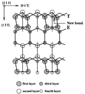
Ref. 12, the energy difference between the two surface re-constructions is rather small and is at the level of accuracy of these calculations. Hence, depending on the actual experi-mental conditions, one may end up with either surface. An-other reconstruction that was proposed as a possibility for the Si共211兲 surface is a -bonded chain formation as on the Si共111兲 surface. A model for-bonded chain reconstruction on the Si共211兲 surface is shown in Fig. 4, in which the top layer terrace atoms dimerize with the corresponding fourth-layer atoms.18 We investigate this possibility extensively. First, we push down the top layer terrace atoms by⬃1.1 Å so that they are at the same height as the second-layer atoms to facilitate any possible dimerization, and relax the struc-ture. In the optimized structure, the top layer terrace atoms are pushed back up to their original height and the edge atoms form dimers along the 关011¯兴 direction, leading to the 共2⫻1兲 structure. Next, we start from an initial geometry in which the top layer terrace atoms are pushed down substan-tially so that the distance between them and the correspond-ing fourth-layer atoms is ⬃2.3 Å, close to the Si-Si bond length. Then, as a first step, these atoms forming the ‘‘dimer’’ are fixed along with the two lowermost Si layers and the H layer, while all the other atoms are relaxed. The energy of this configuration is found to be higher than that in a共2⫻1兲 reconstructed surface. Starting with this intermediate geom-etry, all the atoms in the top five layers are allowed to move 共including the dimers that were held fixed兲 for further struc-tural optimization. The top layer atoms again move up. The surface ends up in the same 共2⫻1兲 reconstruction with the same energy as obtained starting from an ideal surface. Thus we conclude that the-bonded chain is not a stable recon-struction for this surface.
B. Arsenic adsorption
In this section, we discuss our results of As adsorption on the Si共211兲 surface. Though it has been reported that the clean Si共211兲 can form a rebonded 共1⫻1兲 surface where the edge atoms are missing, none of the adsorption experiments on this surface report this. Also, as noted above, our calcu-lations give a slightly lower surface energy for the 共2⫻1兲 surface. Hence, we have restricted our adsorption studies only to the ideal and the 共2⫻1兲 reconstructed surfaces.
1. As on ideal Si(211)
A stepped surface such as Si共211兲 has many inequivalent atoms on the surface and hence offers a number of possible adsorption sites. We study the adsorption of an As atom on six different symmetry sites on the ideal Si共211兲 surface. These symmetry points are labeled in Fig. 1. The T, E, and Tr sites are on top of the terrace, edge, and trench Si atoms marked in the figure. The trench atoms are the second-layer Si atoms that are also threefold bonded. The bridge site共B兲 is on top of the bond between the surface terrace and edge atoms, while the hollow site 共H兲 is in the middle of the rectangle on the surface formed by two terrace and the two corresponding edge atoms. The valley site 共V兲 is halfway between two second-layer trench atoms. We have selected a set of plausible adsorption sites from our intuitive notions of
chemical bonding. The binding energies of an As atom at various sites and its distance from the nearest Si atoms共s兲 are given in Table V. The B site turns out to be energetically the most favorable one for As adsorption. This is followed by the H, V, E, Tr, and T sites. This sequence of binding energies can be rationalized in the following way. At the B site, the As can bind to the terrace and edge Si. With the edge Si, which has two dangling bonds left, it can form a double bond. The asymmetry in the binding of the As with two surface Si atoms at the T and B sites is clearly seen in the charge-density plot in Fig. 5. This satisfies the dangling bonds of the terrace and edge Si atoms. The As is threefold bonded and its remaining two electrons can from a lone pair. At the H site, the As forms four weak bonds with the four neighboring Si atoms—two terrace and two edge—as can be seen from the larger Si-As bond lengths. However, formation of four bonds reduces the number of dangling bonds. Arsenic is left with one dangling bond and the edge Si atoms with one dangling bond each. The terrace Si’s have their bonds satisfied. This reduction of dangling bonds leads to quite large binding en-ergy at this site. On top of the edge, terrace and trench atoms, the As can bind with only one Si atom. Thus the binding energies are unfavorable at these sites. Out of these three, the binding energy at the E site is the highest. This is presumably because As forms a double bond with the edge Si whereby satisfying its dangling bonds and two of its own. At the T and Tr sites, however, it can form only one bond with the corre-sponding Si atoms as they have only one dangling bond each. This conjecture is supported by the fact that at the E site, the As-Si bond length is the shortest indicating a stron-ger binding. On the other hand, at the V site, the As can form bonds with two neighboring trench Si atoms, which have their remaining dangling bonds satisfied in the process. This makes the binding energy at the V site comparable to that at the B and H sites.
FIG. 4. The proposed-bonded chain reconstruction of Si共211兲 surface. The top layer T atoms bind with the corresponding fourth-layer atoms. Only the top four-fourth-layers have been shown for clarity.
2. As on Si(211)-(2Ã1)
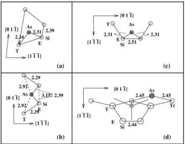
We now discuss our studies of As adsorption on the共2⫻1兲 reconstructed Si共211兲 surface. We have already seen in the case of the ideal surface that the sites on top of various surface atoms, where the As binds to only one Si atom, are not favorable energetically. So we do not consider those sites anymore. We study the adsorption of As on the B, V, and H sites. In addition, we consider As adsorption on top of the surface Si-Si dimer 共D site, see Fig. 2兲. For these calcula-tions, the planar position of the As adatom is held fixed while it is allowed to relax its height. The top five Si layers are fully relaxed as before. On the 共2⫻1兲 reconstructed surface, the V site turns out to be the most favorable one for an As adatom with a binding energy EbV⫽4.84 eV. This is followed by the B, D, and H sites with EbB⫽4.69 eV, EbD⫽4.32 eV, and EbH⫽3.81 eV. The geometries of the surface around the As adatom in these four cases are shown in Fig. 6 . At the V site, As binds with the two neighboring second-layer Si at-oms. Similarity of As adsorption at this site to that on the Si共001兲 surface is noticeable. A monolayer of As adsorbed on Si共001兲 has As-Si bond length equal to 2.44 Å.19As adsorbed on the V site has the same As-Si bond length. At the B site,
the As binds to two surface Si atoms as on an ideal surface. However, it cannot from a double bond with the edge Si as on an ideal surface, since the edge Si is already threefold coordinated because of the Si-Si dimerization. Binding with the As satisfies the dangling bonds of the terrace and edge Si atoms. In spite of having the same dangling-bond density, As adsorbed at the V site has a higher binding energy probably because of the optimal length of the As-Si bond, which is much shorter (⬃2.3 Å) in case of As on the B site. Interest-ingly, the presence of the As adatom at the B site reduces the Si-Si dimer distance marginally to 2.39 Å. At the D site, the As binds with the two edge Si atoms forming the dimer. However, the presence of the As atom in this case increases the Si-Si dimer distance marginally to 2.52 Å, costing en-ergy. This makes the binding energy on this site slightly lower than that at the B site. At the H site, As prefers to form bonds of optimal length with the two edge Si atoms and does not bind with the terrace atoms as can be seen from the interatomic distances shown in Fig. 6. Apparently, this can-not be achieved by keeping all the Si-Si bonds intact. Con-sequently, the Si-Si dimer bond is broken making the Si-Si distance 3.15 Å and costing the Si-Si binding energy. This is in contrast to the behavior of 共2⫻1兲 reconstructed Si共001兲 surface on which As and Te are known to break the Si-Si surface dimers adsorbing on top of the dimers. This breaking of the Si-Si dimers makes the binding at this site the least beneficial energetically. However, it must be noted that though the binding energy at the hollow site is quite low on the共2⫻1兲 surface compared to an ideal one, the total energy is still lower in the former case. We have also studied the effects of a higher coverage of As on the共2⫻1兲 reconstructed Si共211兲 surface. Although the V site turned out to be the most favorable one for an isolated As adsorption, we put the As atoms at the next most favorable site, namely the B site, at higher coverages. This is because, at the V site, the As ada-tom does not have any major effect on the geometry of the surface apart from binding with the two neighboring Tr at-TABLE V. Distances of the As adatom at various symmetry
points on the surface from the neighboring Si atoms of an ideal surface. The corresponding binding energies are also given.
As Distance共Å兲 from which Si
Position E共1兲 E共2兲 T共1兲 T共2兲 Tr共1兲 Tr共2兲 Eb共eV兲
B 2.30 2.30 5.37 H 2.61 2.61 2.61 2.61 5.30 V 2.59 2.59 5.05 E 2.16 4.55 T 2.24 3.85 Tr 2.26 4.28
FIG. 5. Charge-density contour plot in the Si-As-Si plane (y -z plane in our calculation兲 for an isolated As adatom at the B site of an ideal Si共211兲 surface. The asymmetry in bonding of the As with the terrace and edge Si atoms is apparent.
FIG. 6. The local geometry around the adsorbed As atom at the B 共a兲, H 共b兲, D 共c兲, and V 共d兲 sites of the 共2⫻1兲 reconstructed Si共211兲 surface. Please note that the direction of view is slightly different in different cases. All the distances are given in angstrom.
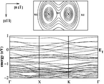
oms. So, a priori it seems that at higher coverage, As atoms, if adsorb at the alternate V sites, would bind with the Tr atoms without causing any change in the reconstruction of the surface. Therefore, at a coverage of 0.5 ML共monolayer兲 that we study, we put four As atoms on the four B sites of the 共4⫻2兲 surface supercell that we use. At 0.5-ML coverage, we find a binding energy of 5.28 eV per As adatom. This is larger than the binding energy of a single As adatom on a B site. With As adatoms on all the B sites, the Si-Si dimer distances decrease to 2.31 Å. This effect was already seen in the presence of a single As atom at a B site. The presence of more As adatoms enhances this effect further. Energy is gained because of stronger binding of the surface Si atoms. Further energy is gained due to dimerization of the As ada-toms. That the As adatoms indeed dimerize at 0.5 ML can be seen from the charge-density plot in the plane of the As atoms shown in Fig. 7. This figure also shows the band struc-ture of the system along directions parallel to the surface. The system is seen to be metallic in character. In the final optimized structure, the Si-As and As-As distances are 2.44 Å and 2.55 Å, respectively, exactly equal to the correspond-ing numbers for As adsorption on the Si共001兲 surface. The
surface still retains the共2⫻1兲 reconstruction at this coverage, but the origin is due to the dimerization of the As adatoms.
C. Te adsorption on Si„211…
In this section, we discuss our studies of Te adsorption on the Si共211兲 surface. As in the case of As adsorption, we study adsorption of Te on the ideal and the 共2⫻1兲 reconstructed surfaces.
1. Te on ideal Si(211)
As in the case of As adsorption, we have studied Te ad-sorption at six special symmetry points on the ideal Si共211兲 surface. These sites can be grouped into two categories in terms of the nature of binding and the binding energies. Three sites, namely the H, V, and B sites, have high binding energies which are close to each other. The T, E, and Tr sites,
TABLE VI. Distances of the Te adatom at various symmetry points on the surface from the neighboring Si atoms of an ideal surface along with the corresponding binding energies.
Te Distance共Å兲 from which Si
Position E共1兲 E共2兲 T共1兲 T共2兲 Tr共1兲 Tr共2兲 Eb共eV兲
B 2.52 2.52 4.15 H 2.80 2.80 2.80 2.80 4.26 V 2.79 2.79 4.19 E 2.38 3.65 T 2.47 3.58 Tr 2.46 3.85
FIG. 7. The top panel shows the charge-density plot in the plane of the As atoms for 0.5-ML coverage. The maximum charge density halfway between the two As atoms at the B sites indicates dimer-ization. The bottom panel shows the band structure of the same system.
FIG. 8. Local geometry around the Te adatom at various sites on a共2⫻1兲 reconstructed Si共211兲 surface: 共a兲 B, 共b兲 H, 共c兲 D, and 共d兲 V sites.
FIG. 9. The top panel shows the charge-density contour plot in the plane of Te atoms for 0.5-ML coverage. Clearly, there is no bonding between the two Te atoms at the B sites. The bottom panel is the band structure of the same system.
on the other hand, have relatively low binding energies. The reason is similar to the case of As. At the H, V, and B sites, the Te binds to four, two and two, Si atoms, respectively. This reduces the number of dangling bonds leading to high binding energies. Why the binding energies at the B and V sites are lower than that at the H site is not obvious. It ap-pears that the bond-bending energy of the edge Si atom for a Te at B is rather high. For an As at B, further energy can be gained by forming a double bond with the edge atom which is not possible for a Te adatom. It should also be mentioned that the binding energies at the V and B sites are very close and their difference is within the error margins of our calcu-lation. This is in agreement with the experimental observa-tion of Dhar et al.11 mentioned before. However, they have no precise information of the binding sites because of the nature of their experiments. For a Te on top of the T, E, and Tr Si atoms, the Te adatom can bind to only one Si atom and thereby have low binding energies. The binding energies and the distances from the nearest Si atoms are given in Table VI.
2. Te on Si(211)-(2Ã1)
Now we discuss our studies of Te adsorption on the共2⫻1兲 reconstructed Si共211兲 surface. Again, we study adsorption only on the four sites where the Te adatom can bind to more than one Si atoms, i.e., the B, H, V, and D sites. The B site is found to be energetically the most favorable one for Te ad-sorption with a binding energy of EbB⫽4.09 eV, which is closely followed by the V site with EbV⫽4.02 eV. The D and H sites have relatively lower binding energies with EbD ⫽3.32 eV and Eb
H⫽2.62 eV, respectively. It should be men-tioned here that the maximum binding-energy values for Te on Si共211兲 found in our calculation are slightly different from that obtained by Dhar et al.11However, that is not sur-prising given the fact that ours is a complete quantum-mechanical calculation while their estimate is based on purely classical considerations. Unlike in the case of As, the Si-Si dimer is not broken for a Te adsorption on the H site. If the As-Si bond is stronger than the Si-Si bond, the surface Si dimers can break in favor of the Si atoms forming double bonds with the adsorbed As thereby gaining energy. This is not possible in the case of Te which has a valence of 2 and hence the Si dimer remains intact. The geometries around the adsorbed Te atom in these four cases are shown in Fig. 8. We have also studied 0.5-ML Te adsorption on the共2⫻1兲 recon-structed Si共211兲 surface. Since the B site is the most favor-able for Te adsorption, it is reasonfavor-able to put the additional Te atoms on the B sites as well. Hence, we have studied the effects of four Te adatoms at the four B sites in our 共4⫻2兲 surface supercell just as in the case of As. In marked contrast
to As adsorption, the Te atoms do not dimerize as can be seen from the charge-density contour plots in the plane of Te at-oms shown in Fig. 9. This figure also shows the band struc-ture of the 0.5-ML Te-covered surface. As can be seen, this system is also metallic in character. The binding energy of 4.09 eV per Te adatom is almost the same as for a single Te adatom 共4.08 eV兲. This is consistent with the fact that there is no additional energy gain, unlike the case of As, from adatom dimerization. Moreover, it is also consistent with the chemical notion that Te, having the outermost electronic con-figuration of 5s25 p4, is divalent and cannot dimerize after binding with two neighboring Si atoms. This absence of Te-Te dimerization is exactly similar to the case of 1-ML Te adsorption on the Si共001兲 surface.20However, in case of the Si共211兲 surface, the 共2⫻1兲 reconstruction of the substrate is retained because the edge Si atoms retain their dimerization. In the optimized structure, the Si-Si dimer distance on the surface is found to be 2.35 Å; and the Si-Te distance is 2.56 Å. The Si-Te distance is very close to the sum of the atomic radii of Si (⬃1.17 Å) and Te (⬃1.32 Å) and the value for the same quantity found for Te adsorption on the Si共001兲 surface. Note that we have not tried to study coverages be-yond 0.5 ML because of the additional complication of sub-surface adsorption for coverages greater than 0.6 ML, as seen in Ref. 11.
IV. CONCLUSION
We have performed an extensive plane-wave, pseudopo-tential density-functional calculations for the electronic and structural properties of the clean and As- and Te-covered Si共211兲 surface. The clean surface readily forms a 共2⫻1兲 reconstruction through dimerization of the edge atoms along the关011¯兴 direction. A rebonded 共1⫻1兲 surface is also found, but the-bonded chain is not a stable reconstruction for this surface. The twofold bridge site is found to be the most favorable one for an isolated As adatom, whereas the four-fold hollow site is the most favorable one for a Te on an ideal Si共211兲 surface. On the 共2⫻1兲 reconstructed surface, the val-ley site is the most favorable one for As while the bridge site is the most favorable one for an isolated Te. Just as suggested by the experiments on Br and Te adsorption on the Si共211兲 surface, there are more than one points on the surface with very close binding-energy values for both As and Te. At 0.5-ML coverage, when there is a line of adatoms along 关011¯兴 at the bridge sites, the As adatoms dimerize on the Si共211兲 surface while Te adatoms do not. In this respect, their behavior is very similar to that on the Si共001兲 surface. Both 0.5-ML As- and Te-covered surfaces are found to be metallic in character.
1D.J. Chadi, Phys. Rev. B 29, 785共1984兲.
2B.Z. Olshanetsky and V.I. Mashanov, Surf. Sci. 111, 414共1981兲. 3S.L. Wright, H. Kroemer, and M. Inada, J. Appl. Phys. 55, 2916
共1984兲.
4S. Rujirawat, L.A. Almeida, Y.P. Chen, S. Sivananthan, and D.J.
Smith, Appl. Phys. Lett. 71, 1810共1997兲.
5B. Yang, Y. Xin, S. Rujirawat, N.D. Browning, and S.
6T. Berghaus, A. Brodee, H. Neddermeyer, and S. Tosch, Surf. Sci.
184, 273共1987兲.
7X. Wang and W.H. Weinberg, Surf. Sci. 314, 71共1994兲. 8
R. Kaplan, Surf. Sci. 116, 104共1982兲.
9Y. Yang and E.D. Williams, Surf. Sci. 215, 102共1989兲.
10E.G. Michel, V. Etela¨niemi, and G. Materlik, Surf. Sci. 269, 89
共1992兲.
11N.K. Dhar, N. Goldsman, and C.E.C. Wood, Phys. Rev. B 61,
8256共2000兲.
12C.H. Grein, J. Cryst. Growth 180, 54共1997兲. 13S. Mankefors, Surf. Sci. 443, 99共1999兲.
14D. Vanderbilt, Phys. Rev. B 41, 7892共1990兲; G. Kresse and J.
Hafner, J. Phys.: Condens. Matter 6, 8245共1994兲.
15J.P. Perdew and Y. Wang, Phys. Rev. B 46, 6671共1992兲. 16G. Kresse and J. Hafner, Phys. Rev. B 47, R558共1993兲; G. Kresse
and J. Furtmu¨ller, ibid. 54, 11 169共1996兲.
17K.C. Pandey, in Proceedings of the 16th International Conference
on the Physics of Semiconductors, edited by M. Averous 共North-Holland, Amsterdam, 1983兲, p. 761.
18K.C. Pandey, Phys. Rev. Lett. 47, 1913共1981兲; J.E. Northrup and
M.L. Cohen, ibid. 49, 1349共1982兲.
19R.I.G. Uhrberg, R.D. Bringans, R.Z. Bachrach, and J.E. Northrup,
Phys. Rev. Lett. 56, 520共1986兲.
20
P. Sen, S. Ciraci, I.P. Batra, C.H. Grein, and S. Sivananthan, Surf. Sci. 519, 79共2002兲.