Journal of Micromechanics and Microengineering
PAPER
A simple approach for the fabrication of 3D
microelectrodes for impedimetric sensing
To cite this article: Mustafa Tahsin Guler et al 2015 J. Micromech. Microeng. 25 095019
View the article online for updates and enhancements.
Related content
A review of microfabrication techniques and dielectrophoretic microdevices for particle manipulation and separation
M Li, W H Li, J Zhang et al.
-A microfluidic multichannel resistive pulse sensor using frequency division multiplexing
Ashish V Jagtiani, Joan Carletta and Jiang Zhe
-Challenges and trends in magnetic sensor integration with microfluidics for biomedical applications
S Cardoso, D C Leitao, T M Dias et al.
-Recent citations
Micropatterning of planar metal electrodes by vacuum filling microfluidic channel geometries
Stelios Chatzimichail et al
-Controllable alignment of elongated microorganisms in 3D microspace using electrofluidic devices manufactured by hybrid femtosecond laser microfabrication
Jian Xu et al
-1. Introduction
The detection of particles with microfluidic devices is mainly achieved using either electrical or optical techniques. In par-allel to the advancements in microfabrication techniques, electrical sensing methods have evolved rapidly in the last few decades [1]. The widespread use of electrical sensing has given rise to many different methods for the fabrication of microelectrodes. The fabrication of coplanar electrodes using conventional microfabrication techniques is the most common
method to integrate electrodes with microfluidic devices. Apart from particle detection, the use of microelectrodes in microfluidic systems has opened up a plethora of applications such as dielectrophoresis [2–5], electro-osmotic pumps [6], protein analysis [7, 8], electroporation [9] and electrorotation systems [10].
For electrical particle detection in microchannels, sen-sitivity can be improved using identical top and bottom electrodes to form a uniform three-dimensional (3D) electric field in the microchannels [11]. It has been demonstrated that
2 Science and Technology Application and Research Center, Aksaray University, 68100 Aksaray, Turkey 3 UNAM-National Nanotechnology Research Center, Institute of Materials Science and Nanotechnology,
Bilkent University, 06800 Ankara, Turkey
E-mail: [email protected], [email protected], [email protected] and elbuken@unam. bilkent.edu.tr
Received 11 March 2015, revised 29 June 2015 Accepted for publication 13 July 2015 Published 21 August 2015
Abstract
In this paper, we present a very simple method to fabricate three-dimensional (3D) microelectrodes integrated with microfluidic devices. We form the electrodes by etching a microwire placed across a microchannel. For precise control of the electrode spacing, we employ a hydrodynamic focusing microfluidic device and control the width of the etching solution stream. The focused widths of the etchant solution and the etching time determine the gap formed between the electrodes. Using the same microfluidic device, we can fabricate integrated 3D electrodes with different electrode gaps. We have demonstrated the functionality of these electrodes using an impedimetric particle counting setup. Using 3D microelectrodes with a diameter of 25 μm, we have detected 6 μm-diameter polystyrene beads in a buffer solution as well as erythrocytes in a PBS solution. We study the effect of electrode spacing on the signal-to-noise ratio of the impedance signal and we demonstrate that the smaller the electrode spacing the higher the signal obtained from a single microparticle. The sample stream is introduced to the system using the same hydrodynamic focusing device, which ensures the alignment of the sample in between the electrodes. Utilising a 3D hydrodynamic focusing approach, we force all the particles to go through the sensing region of the electrodes. This fabrication scheme not only provides a very low-cost and easy method for rapid prototyping, but which can also be used for applications requiring 3D electric field focused through a narrow section of the microchannel. Keywords: microfluidic electrical sensing, 3D microelectrodes, flow-focusing, particle counting, microfabrication
S Online supplementary data available from stacks.iop.org/JMM/25/095019/mmedia
(Some figures may appear in colour only in the online journal)
M Tahsin Guler et al Printed in the UK 095019 JMM 0960-1317 10.1088/0960-1317/25/9/095019
Papers
9such electrodes increase the signal by approximately 40% compared to coplanar electrodes. The use of 3D electrodes has also proven useful for dielectrophoretic applications [12]. Recently, a new fabrication scheme was demonstrated to have homogeneous electric field distribution in microchannels by integrating coplanar electrodes in the side walls of microchan-nels [13]. However, the fabrication of such electrodes requires multiple steps and precise alignment, which increases com-plexity. Such uniform electric fields can be generated by 3D metal electrodes using some other techniques including elec-troplating [14, 15], micropowder injection molding [16, 17], microsolidics [18, 19], screen printing [20–22] and microscale electro-discharge machining [23].
In this study, we present a simple approach for the fab-rication of 3D microelectrodes. We form 3D electrodes by etching a microwire, which is placed across a microchannel, and using a flow focusing microfluidic design. Once the mold for the fabrication of the microfluidic channel is obtained, the rest of the fabrication can be performed in a standard labora-tory in less than thirty minutes and does not require any clean room processes. We can form self-aligned 3D microelectrodes using standard laboratory equipment in less than thirty min-utes. The spacing of the electrodes can be very well controlled using a flow focusing geometry. Large contact pads were fabricated using silver paste and aluminium foil in order to facilitate electrical connections and to minimise the issues due to contact resistance. Another benefit of this method is that the amount of wasted metal is minimised due to the subtractive nature of the process. For a single pair of electrodes, we used 2.5 cm long gold wire 25 μm in diameter. In terms of sim-plicity, our approach is similar to the multiphase laminar flow patterning method demonstrated by Whitesides’ Group. They demonstrated the formation of thin metallic or non-metallic structures by chemical reactions occurring at the interface of fluids at the laminar flow regime [24].
In addition to its simplicity, our method provides elec-trodes that have very high conductivity and that can be utilised for applications requiring high voltages and high frequencies. Bond wires of different radii can be selected depending on the required signal intensity. The same method can also be applied at the nanoscale and sub-micron size electrodes can be fabricated with the use of nanowires, which has been a rap-idly advancing technology in recent years [25, 26]. Combined with the benefits of soft lithography, this technique provides a very low-cost and rapid way of generating perfectly aligned 3D electrodes in microchannels.
In this study, we have demonstrated the performance of our low-cost 3D electrodes using an impedimetric particle counting setup. The focusing of particles through the sensing region is an important requirement for impedimetric sensing for enhanced sensitivity. Hydrodynamic flow focusing is one of the most common methods to achieve the alignment of par-ticles with the microelectrodes [27, 28]. Our 3D electrodes are especially advantageous for such purposes. Since the elec-trodes are already defined with a flow-focusing microfluidic channel, the use of the same channels with the same flow rate ensures the alignment of the sample stream with the sensing region of the electrodes. These self-aligned electrodes can
also be very effectively used for other biological applications such as electrical cell lysis [29–31], electrochemical detection [32] and electroporation [33].
2. Materials and methods 2.1. Device fabrication
The fabrication of the electrode integrated microfluidic devices is accomplished in three steps. First, PDMS (polydimethyl-siloxane) microchannels are fabricated using standard soft lithography techniques [34]. For the impedance sensing of 5–10 μm diameter particles, we fabricated channels 50 μm in height and 200 μm in width. The mold is fabricated on a 4 inch silicon substrate using SU-8 2050 photoresist. The mold fab-rication is the only step of the fabfab-rication that was performed in the cleanroom.
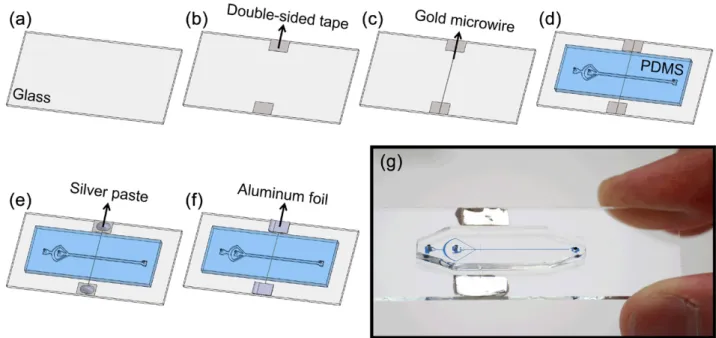
Secondly, the microwire to be etched is fixed onto a glass slide and covered with the microfluidic channel as summa-rised in figure 1. This process starts by cleaning the glass slide by successive acetone, isopropyl alcohol and deionised (DI) water washes followed by air drying. After dehydration baking at 100 °C for 5 min, two small pieces of double-sided tape are attached to the glass slide to hold the microwire in place. Then, 25 μm diameter gold microwire (Good Fellow AU005120) is stretched between the double-sided tapes and attached to the glass slide. Afterwards, the PDMS channel is bonded to the glass slide by plasma activation (figure 1(d )). Care should be taken at this stage to ensure that the micro-channel is perpendicularly aligned with the microwire on the glass slide. Then, the bonded device is placed on a hot plate at 100 °C for 45 min. This heating step enhances the bonding of the device and also pre-heats the device before sealing the gap along the two sides of the microwire. The 25 μm thick microwire causes the PDMS block on top of it to bulge out and to leave an air gap crossing the microchannel. After pre-heating the device at 100 °C, the device is placed on a flat insulating surface and 50 μl of PDMS solution (mixed at 10:1 ratio and degassed) is pipetted along the two edges of the electrode from both sides of the glass slide. This uncured PDMS drop advances into the gap by capillary action. We observe the progress of the PDMS solution front edge along the capillary air gap. When the PDMS reaches the midway in the air gap we place the device on the hot plate at 100 °C for an additional 15 min. This is the most critical step for the fabrication of the integrated 3D microelectrodes. The amount of PDMS drop and pre-heating temperature may vary depending on the thickness of the top PDMS layer as well as the thickness of the microwire used. We tested the bonding strength of our devices using an adjustable pressure source. For the maximum pressure of 2 bar that we can apply, we did not observe any leakage. Finally, contact pads are formed by putting silver paste (EMS 12640) on the two edges of the microwire and placing small pieces of aluminium foil over them. After air drying the silver paste for 30 min, rigid con-tact pads were achieved. The integrity of the microwire and the contacts are verified by electrical continuity test probing the two aluminium contacts using a multimeter.
The fabrication of the device is completed by etching the gold microwire using aqua regia solution prepared at a 3:1 v/v ratio of hydrochloric acid (HCl) and nitric acid (HNO3, Sigma). The etching solution is heated to 50 °C in a glass vial before being introduced to the microchannel. Then, the etching solution is introduced in the microchannel using a syringe pump for 2 min at a flow rate of 40 μl min−1. The portion of the electrodes over-lapping with the microchannel is etched resulting in an electrode pair, as shown in figure 2. After the etching of the electrodes is completed, DI water is flushed to wash out the etching solution. As can be seen in the microscope image of the electrodes, the spacing between the electrodes is 315 μm. During the fabrica-tion of several devices, we realised that it is difficult to control the spacing of the electrodes using this method. Although the same process parameters are used, we observed that the spacing between the electrodes varies from chip to chip. In addition, heating the etching solution generates bubbles in the solution which disturbs the continuous etching of the microwires.
In order to solve these problems, we have improved our final fabrication step using a hydrodynamic flow focusing geometry. The etching solution was focused at the centre of the channel using DI flow streams, as shown in figure 3. Rather than heating the etchant, we heated the DI solution and the assembled device to a temperature of 90 °C. It is advised that for long etching times, it is very important to keep the device at high temperature since convection cooling decreases the etching rate of the microwire. The solutions were pumped from the two inlets using tygon tubing (Cole Parmer) and a pres-sure pump (Elveflow OB1). The inlet prespres-sures for DI water and etching solution were set as 80 mbar and 90 mbar, respec-tively. The formation of the electrodes was monitored with an inverted microscope. Figure 4 shows the time-lapse images of the etching of the microelectrodes. It can be seen that the spacing of the electrodes can be adjusted by fine-tuning the focused stream width and the etching time. The pre-heating
temperature is another parameter that affects the etching pro-cess. It was observed that keeping the etching solution at room temperature is very helpful in eliminating bubble generation. A sample video demonstrating the etching process is provided as supplementary data (stacks.iop.org/JMM/25/095019/mmedia).
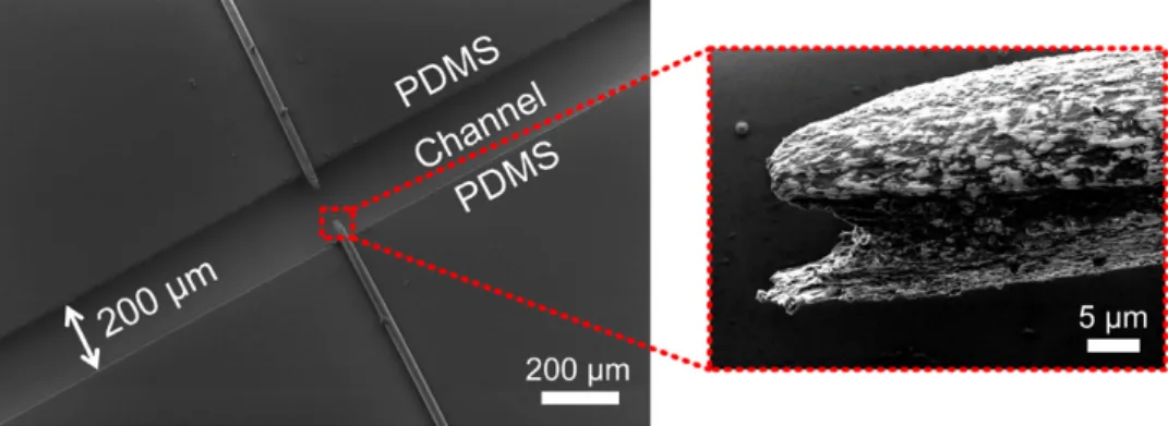
After the desired electrode spacing is obtained, the chip is flushed with DI water and air dried for 12 h. It was observed that swelling of the PDMS with etchant causes the channel to par-tially lose its optical transparency during the etching process. The 12 h dry incubation of the finalised device helps it recover its optical transparency, which might be critical for certain applications. The scanning electron microscope (SEM) images of the etched microwires can be seen in figure 5. The shape of the tip of the electrode is an indication of the flow profile of the etching solution in the microchannel.
2.2. Impedimetric sensing
We have demonstrated the functionality of the microfabri-cated electrodes through an impedimetric sensing experiment. Figure 1. Chip fabrication steps: (a) a cleaned glass slide, (b) attaching the double-sided tapes, (c) stretching the gold microwire between the tapes, (d ) bonding the PDMS microchannel onto the glass slide, (e) placing the silver paste onto the tapes, ( f ) covering the silver paste with aluminum foil, (g) a picture of the fabricated device.
Impedimetric sensing enables the label free detection of mic-roparticles and biological substances. Although the resolving power of impedimetric detection is limited compared to the
state-of-the-art optical flow cytometers with detection capa-bilities at multiple wavelengths, it is a very practical approach especially for the detection of particles from a less diverse Figure 4. Time-lapse optical microscope images of the etching of gold microwire electrodes using the flow-focused aqua regia solution.
Figure 5. Scanning electron microscope (SEM) image of the microfabricated electrodes with the inset showing a close-up image of the tip of an etched electrode.
Figure 3. Schematic (a) and optical microscope image (b) of a hydrodynamic flow-focusing device for the controlled etching of microelectrodes.
population. Unlike optical detection techniques, electrical detection does not require any bulky or costly components. The use of a single metal wire as an electrical sensor reduces the complexity significantly. In this section, we summarise our results on the impedimetric sensing of microbeads and erythrocytes using our 3D microelectrodes.
2.3. Measurement setup
In previous studies, impedance sensing in microfluidic sys-tems were mostly demonstrated using lock-in amplifiers and custom-made electronic circuitries [11, 35]. There are only a few studies that use off-the-shelf devices for impedimetric sensing [14, 36, 37]. However, the sensitivity achieved by these systems is limited as compared to the high-end lock-in amplifier detection systems. Thanks to our 3D electrodes, we are able to detect 6 μm diameter polystyrene microbeads (Polysciences) and erythrocytes by an LCR meter without using any additional electronics. The 3D electrodes focus the electric field lines through a very narrow region, at which the sample solution is also aligned with the use of flow-focusing microchannels. Since the electrodes are generated using the same geometry and the same flow parameters, the particles are very effectively focused between the electrodes. This yielded very high sensitivity compared to the conventional coplanar electrodes that require several cleanroom fabrication steps.
We used an LCR meter (Agilent E4980A) for our imped-imetric experiments. The system was controlled with a custom-developed LabView code and provided real-time results at a sampling rate of 184 Hz. The electrical connection between the LCR meter and the device was made by BNC connectors and RG59 coaxial cables. During the experiments, the microscope stage, BNC connectors and the solutions were kept grounded.
The LCR meter provides measurements of complex imped-ance as Z–θ values at a wide frequency range (from 20 Hz to 2 MHz) with peak-to-peak voltages of up to 15 V. It is impor-tant to determine the optimum measurement frequency and voltage that yield the highest signal-to-noise ratio. Our initial experiments demonstrated that the signal-to-noise level for the
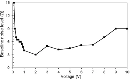
impedance measurement (|Z|) of polystyrene microbeads is the highest at a 2 MHz excitation frequency. We also observed that the signal level for microbeads is approximately 6 Ω irrespec-tive of the operation voltage. Modifying the operation voltage changes the noise level, whereas the 6 Ω signal from the beads does not change considerably. Therefore, in order to determine the optimum operation voltage, we focused on minimising the baseline noise level which is quantified as the peak-to-peak variation between the highest and the lowest reading. We performed voltage sweep experiments using 0.2 M NaCl solution without any microbeads and noted the baseline noise level for the electrode we fabricated using the hydrodynamic flow-focusing device shown in figure 4. Figure 6 shows the noise level measured for each excitation voltage. For any set voltage value, we recorded the baseline signal for 1 min and determined the maximum peak-to-peak variation, which is shown as the baseline noise level (Ω) in figure 6. The voltage dependence of the noise level did not show a linear depend-ence. Based on these results we picked 2 Vpp as the excitation signal amplitude to maximise the signal-to-noise ratio.
These voltage sweep measurements demonstrated another advantage of our 3D microelectrodes. During our experiments using the 3D electrodes, we did not observe any deterioration of the electrodes over the course of the experiment, even when high voltages were applied. On the other hand, a similar meas-urement performed using coplanar electrodes with a 0.2 M buffer solution showed significant electrode damage. Voltages higher than 1 Vpp led to the rapid deterioration of the electrodes when they were activated over a few minutes. The voltage dependency of this phenomenon is a sign of the electrochem-ical character of the corrosion. These results suggest that this new fabrication scheme provides durable 3D electrodes as compared to the conventional thin film metal electrodes. 3. Results and discussion
3.1. Microbead detection
For the impedimetric detection of microparticles, we fab-ricated four devices with different electrode gaps by simply Figure 6. The maximum peak-to-peak variation of noise for a 3D electrode generated by hydrodynamic focusing tested at different excitation voltages. The noise level for each excitation voltage is determined from a 1 min recording of the signal.
changing the relative flow rates at the inlet of the microflu-idic device (figure 7). We increased the electrode gap by incrementing the inlet pressure for the etching solution from 70 mbar to 95 mbar while keeping the pressure for the DI solution inlet constant at 80 mbar. Our new 3D electrode fabrication scheme eliminates the need for costly and time-consuming mask fabrication and lithography processes.
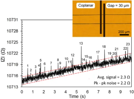
We also fabricated coplanar electrodes as a reference sensor. The coplanar electrodes were fabricated on a glass slide using the lift-off method. After spin coating and pho-tolithographic patterning of the positive photoresist (AZ 5214), 15 nm Cr and 50 nm Au were deposited using thermal evaporation (Vaksis). The process was completed by lift-off in acetone using an ultrasonic shaker. The fabricated elec-trodes are shown in figure 8. The width and the spacing of the electrodes is 30 μm. The bonding of these electrodes with the PDMS microchannel was accomplished under microscope by plasma cleaning of both surfaces.
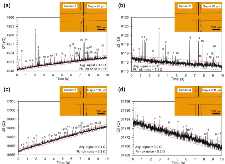
Figure 7 shows the |Z| value that we measured at 2 MHz and 2 Vpp excitation signal using a 0.2 M NaCl solution con-taining 6 μm diameter polystyrene beads. The results were obtained by using 25 μm diameter electrodes with electrode gaps of 20 μm, 70 μm, 150 μm and 200 μm (figures 7(a)–(d), respectively).
It can be seen that the signal level depends on the gap between the electrodes. As the gap is increased from 20 μm to 200 μm the baseline impedance increases from approxi-mately 5 kΩ to 32 kΩ. In agreement with our previous measurements, the noise level for the 3D microwire sensors depends on the baseline impedance. The sensor with a 20 μm electrode gap yields the least noise out of these four sensors. The peaks corresponding to the microbeads passing through the sensing region can be distinguished from the noise level. During these measurements, we also monitored these sen-sors under a microscope and counted the beads going through the sensor. The peaks corresponding to the microbeads are numbered in figure 7. In order to compare the performance of different electrodes we define signal-to-noise ratio (SNR) as the ratio of the average peak height (Avg. signal) to the peak-to-peak noise variation (Pk–pk noise) for the 10 s meas-urements shown in figure 7. We observed that sensor 4 (with 200 μm electrode gap) has the lowest SNR of 0.76. During the 10 s measurement interval shown in figure 7(d), although 58 beads passed through the sensor, only 15 of them gave peaks that can be distinguished from the noise. On the other hand, sensor 1 (with a 20 μm electrode gap), figure 7(a), captured 31 beads out of the 63 beads which passed through the sensor and yielded the highest SNR value as 3.1.
Figure 7. Impedimetric detection of microbeads using 3D microwire electrodes. The peaks represent polystyrene microbeads (6 μm diameter) passing through the sensing region. The sensors have different electrode gap distances of (a) 20 μm, (b) 70 μm, (c) 150 μm and (d ) 200 μm.
During these measurements, we also observed that the microbead’s position in the microchannel is an important parameter for changing the signal height. Microbeads travel-ling close to one of the electrodes, i.e. away from the focused flow centerline, gave the highest signal intensities. Another reason for the variation in signal height is the sampling frequency. Although 184 Hz is a relatively high sampling frequency for benchtop LCR meters, it is significantly lower than advanced impedance detection systems, which provide signals at a rate of kHz.
A similar measurement was performed with coplanar elec-trodes using the same bead solution. The results are shown in figure 8. It can be seen that the sensitivity of the coplanar electrodes (SNR = 1.05) is similar to the 3D microwire sensor with an electrode gap of 150 μm (figure 7(c), SNR = 1.16). The coplanar sensor detected 23 microbeads out of the 61 microbeads which passed through the microchannel. This comparison demonstrated that focusing the electric field lines in a narrower region using the 3D microelectrodes yields better results in terms of the signal-to-noise ratio. The gap between the electrodes can be very easily controlled by the width of the hydrodynamically focused etching solution, as shown in the supplementary movie file (stacks.iop.org/JMM/25/095019/ mmedia).
3.2. Erythrocyte counting
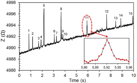
After the characterisation of our 3D electrodes using micro-beads, we used the electrodes with 20 μm spacing (figure 7(a)) for counting the erythrocytes. A blood sample was obtained from a donor with their informed consent. The venous blood was stored in a vacuum tube (1/9 volume of 3.8% sodium citrate) and utilised within 4 h after the blood had been taken. 5 μl of whole blood was diluted in 10 ml of phosphate buff-ered saline (PBS). The erythrocyte concentration in this solution was measured by a hemocytometer as 0.2 × 10⁶
cells ml−1. Then, the sample solution was introduced to the system using PBS as the focusing solution. The inlet pres-sures for the sample and PBS were chosen as 15 mbar and 12 mbar, respectively, which are proportional to the pressures used during the fabrication of the electrodes. This ensures perfect alignment of the sample solution through the sensing region between the 3D electrodes. These pressures yielded a total flow rate of approximately 0.5 μl min−1. Figure 9 shows the signal obtained from the erythrocyte containing solution. During these experiments, the device was monitored under a microscope and each peak obtained by the sensor was veri-fied by visual observation. Out of the 25 erythrocytes passing from the sensor, 15 of them were detected. Both our measure-ments with microbeads and erythrocytes show that there is a variation in the signal height corresponding to each detected particle. We hypothesise that this is due to the orientation of the particles as they pass through the sensing region. The biconcave shape of the erythrocytes may yield more variation due to their differing orientation as compared to the micro-spheres. The inset in figure 9 shows the signal obtained from a single cell. As seen from this figure, each cell is sampled by 7 or 8 signals. Increasing the data rate would decrease the variation in the signal, but there still might be a signal varia-tion due to the posivaria-tion and orientavaria-tion of the particles in the sensing region.
3.3. Limitations of the 3D microwire sensor
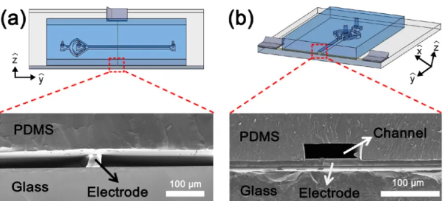
The results in the previous section demonstrate that 3D microwire sensors can detect micrometre size particles in microchannels. However, due to the deformed shape of the upper PDMS layer, there is a section of the microchannel that goes over the sensing region formed by the microwire electrodes. This region occurs due to the thickness of the microwire. For our system, we used a 25 μm diameter microwire and a 50 μm deep microchannel. After bonding, Figure 8. Impedimetric detection of microbeads using conventional microfabricated coplanar electrodes.
the PDMS section that overlaps with the microwire bulges out and forms a 50 μm thick region above the sensing region. This is schematically shown in figure 10. During our impedimetric measurements the sample stream is focused laterally with a buffer solution. However, there are still some particles that go over the sensing region, as demonstrated in figure 10(b). This is one of the inherent limitations of our fabrication scheme. There are several approaches that can be used to eliminate this shortcoming.
One way to overcome this problem might be to have grooves on the PDMS channels. Such grooves can be easily fabricated during the master fabrication and can be defined during the photolithography step together with the microchan-nels. The dimensions of these grooves should be matched with the microwires so that the wires sit in a recess. This approach would require the placement of the microwire in the recess during fabrication. Also, the molds fabricated using this approach will be compatible with wires of a certain thickness.
Another way of ensuring all particles go through the sensing region might be to physically push the particles towards the bottom of the microchannel so that they travel across the electric field lines generated by the 3D microwire sensor. Such a modification can be achieved by dynamically changing the height of the channel using multilayer soft lithography [38]. However, this approach complicates the
fabrication of the microfluidic device and requires several off-chip components.
Instead, we employed hydrodynamic flow-focusing to push the sample stream downwards in the channel. The cross-sectional SEM images of the air gap region and the microchannel over the microwire electrodes of our devices are shown in figure 11. In figure 11(b), the microwire (25 μm diameter) under the microchannel (50 μm height) is shown before the etching process. After etching the electrodes, the channel height increases to 75 μm in the sensing region and it is necessary to push down the particles by at least 50 μm. 3D hydrodynamic focusing is a very practical way of achieving this goal. The 3D focusing of solutions has been demonstrated using different mechanisms [28, 39–42]. Among those exam-ples, the method shown by Watkins et al is relatively easy to implement, since it does not require advanced manufacturing capabilities [41]. They achieved focusing of the solution in both lateral and vertical dimensions by using two inlets for the focusing fluid. After the fluid is horizontally focused another inlet is punched and the fluid stream is pushed down, as shown in figure 12(a). We used a similar mechanism to hydrodynam-ically focus the sample stream strictly between the electrodes. We punched a 0.5 mm diameter inlet upstream of the sensing region. The flow rates were controlled using a pressure pump. We tested 3D fluid focusing by using yellow and blue dye Figure 9. Impedimetric detection of erythrocytes in PBS solution using a 3D microwire sensor with an electrode gap of 20 μm.
Figure 10. (a) Representative 3D drawing showing the shape of the channel in the sensing region. (b) Representative cross-sectional view near the electrode: bulging of the channel top layer causes some particles to pass through the sensor undetected.
solutions to focus the DI water sample vertically and horizon-tally, respectively.
In order to ensure that sample stream is completely focused between the electrodes the flow rate for the 3D focusing solu-tion should be twice the value of the flow rate in the main channel. Then, the 50 μm portion of the 75 μm height channel will be occupied by the 3D focusing solution and the sample will be restricted to the bottom 25 μm of the channel, which corresponds to the height of the electrodes. We performed a hydrodynamic circuit analysis and determined the flow rates for the 2D focusing solution, sample solution and 3D focusing solution as 61 mbar, 57 mbar and 50 mbar, respectively. When these pressures were applied, we obtained the 3D focusing, as shown in figure 12(b). When the inlet pressure for the 3D focusing solution was decreased to 45 mbar, we obtained the 2D focusing state shown in figure 12(c). The pressure values that yield the optimum flow focusing requires some tuning and can best be achieved using a pressure controlled system. As seen in figure 12(b), the yellow focusing stream goes over
the laterally focused flow without disturbing the focused sample flow.
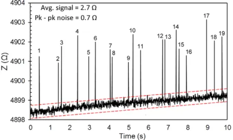
After improving our focusing performance we repeated the impedimetric measurement of microbead detection using the system shown in figure 12. The results are shown in figure 13. We used a microbead solution with the same bead concentration as our previous experiments and observed the microbeads through a microscope during the experiment. For the results shown in figure 13, out of 48 microbeads 19 of them are detected using the electrodes with a spacing of 20 μm. Comparing the data we obtained from 3D hydrody-namic focusing (figure 13) and 2D hydrodynamic focusing (figure 7(a)), one can see that the variation in the signal is significantly reduced. We believe this is due to the fact that the particles are pushed all the way down in the sensing region and centered very well with the 3D microwire elec-trodes. The signal-to-noise ratio for 3D focused particles is 3.9. However, our system still falls short from detecting all the particles due to the low sampling rate of our detection Figure 12. (a) Schematic of the device used for the 3D hydrodynamic focusing of the sample solution. (b) Microscope image showing that the sample stream with yellow dye was focused in 3D using the additional inlet punched between the lateral focusing section and the microwire electrodes. (c) Microscope image showing that the sample stream was 2D focused by changing the flow rates.
system. We performed all of our experiments at a sampling rate of 184 Hz. Focusing the sample solution from upwards using a secondary focusing solution inlet increases the flow rate of the microbeads. This decreases the residence time of each particle in the sensing domain of our electrodes and blinds the system to some of the particles. We tried to slow down the particles by decreasing the inlet pressures while keeping the flow rate ratio of the solutions the same. However, we were unable to achieve successful 3D hydro-dynamic focusing at lower flow rates. Performing the same measurement using a detection system with a higher sam-pling rate would ensure that all the particles are detected using the 3D microwire electrodes.
4. Conclusion
We have reported a novel method of fabricating 3D electrodes integrated with microfluidic devices. The electrodes were fabricated by etching a microwire placed across a micro-channel. The spacing between the wires was finely adjusted by focusing the etching solution in the microchannel using flow-focusing geometry. We exploited these 3D electrodes for the impedimetric detection of particles using a plug and play measurement system. The detection was improved further by focusing the sample stream in 3D between the sensing elec-trodes. This method provides a very low-cost and rapid way of fabricating 3D electrodes that can be utilised for a variety of applications. More importantly, after having a mold for the microfluidic channel this technique eliminates the need for repetitive cleanroom processes for the fabrication of micro-electrodes and provides a new method of integrating micro-electrodes into the standard soft lithography process. An inherent benefit of these electrodes is the fact that they are perfectly aligned with the sample stream when the same flow focusing geom-etry is used for fabrication and testing. By placing multiple microwires in a microchannel and tailoring the flow profile, it is possible to obtain multiple electrodes of different geometry in a single channel.
Acknowledgments
This project was supported by The Scientific and Techno-logical Research Council of Turkey (TUBITAK project no. 112M944) and European Union FP7 Marie Curie Career Inte-gration Grant (no. 322019). The authors also thank Dr Aykutlu Dana, Dr Gokhan Bakan and Amir Ghobadi for their help in the measurement setup and their comments on the manuscript. References
[1] Sun T and Morgan H 2010 Single-cell microfluidic impedance cytometry: a review Microfluid. Nanofluidics 8 423–43 [2] Çetin B and Li D 2011 Dielectrophoresis in microfluidics
technology Electrophoresis 32 2410–27
[3] Choi E, Kim B and Park J 2009 High-throughput microparticle separation using gradient traveling wave dielectrophoresis J. Micromech. Microeng. 19 125014
[4] Chung C-C, Glawdel T, Ren C L and Chang H-C 2015 Combination of ac electroosmosis and dielectrophoresis for particle manipulation on electrically-induced microscale wave structures J. Micromech. Microeng. 25 035003 [5] Khoshmanesh K, Nahavandi S, Baratchi S, Mitchell A and
Kalantar-zadeh K 2011 Dielectrophoretic platforms for bio-microfluidic systems Biosens. Bioelectron. 26 1800–14 [6] Seibel K, Schöler L, Schäfer H and Böhm M 2008 A
programmable planar electroosmotic micropump for lab-on-a-chip applications J. Micromech. Microeng. 18 025008 [7] Tia S and Herr A E 2009 On-chip technologies for
multidimensional separations Lab Chip 9 2524–36
[8] Wang Y, Ye Z, Ping J, Jing S and Ying Y 2014 Development of an aptamer-based impedimetric bioassay using microfluidic system and magnetic separation for protein detection Biosens. Bioelectron. 59 106–11
[9] Ghadami M, Mahjoob M, Shagoshtasbi H and Lee Y 2013 Model-based feedback control of a microfluidic electroporation system J. Micromech. Microeng. 23 125032 [10] Han S-I, Joo Y-D and Han K-H 2013 An electrorotation
technique for measuring the dielectric properties of cells with simultaneous use of negative quadrupolar dielectrophoresis and electrorotation Analyst 138 1529–37 [11] Gawad S, Schild L and Renaud P 2001 Micromachined
impedance spectroscopy flow cytometer for cell analysis and particle sizing Lab Chip 1 76–82
2 639–42
[17] Kim J-S, Jiang K and Chang I 2006 A net shape process for metallic microcomponent fabrication using Al and Cu micro/nano powders J. Micromech. Microeng. 16 48 [18] Siegel A C, Bruzewicz D A, Weibel D B and Whitesides G M
2007 Microsolidics: fabrication of 3D metallic microstructures in Poly (dimethylsiloxane) Adv. Mater. 19 727–33
[19] So J-H and Dickey M D 2011 Inherently aligned microfluidic electrodes composed of liquid metal Lab Chip 11 905–11 [20] Li M, Li Y-T, Li D-W and Long Y-T 2012 Recent
developments and applications of screen-printed electrodes in environmental assays—a review Anal. Chim. Acta 734 31–44
[21] Kim S, Park J-h, Kang K, Park C-O and Park I 2015 Direct metal micropatterning on needle-type structures towards bioimpedance and chemical sensing applications J. Micromech. Microeng. 25 015002
[22] Pyo S, Lee J-I, Kim M-O, Chung T, Oh Y, Lim S-C, Park J and Kim J 2014 Development of a flexible three-axis tactile sensor based on screen-printed carbon nanotube-polymer composite J. Micromech. Microeng. 24 075012
[23] Lim H, Wong Y, Rahman M and Edwin Lee M 2003 A study on the machining of high-aspect ratio micro-structures using micro-EDM J. Mater. Process. Technol. 140 318–25 [24] Kenis P J, Ismagilov R F and Whitesides G M 1999
Microfabrication inside capillaries using multiphase laminar flow patterning Science 285 83–5
[25] Arkan E F, Sacchetto D, Yildiz I, Leblebici Y and Alaca B E 2011 Monolithic integration of Si nanowires with metallic electrodes: NEMS resonator and switch applications J. Micromech. Microeng. 21 125018
[32] Yang L, Li Y and Erf G F 2004 Interdigitated array microelectrode-based electrochemical impedance immunosensor for detection of Escherichia coli O157: H7 Anal. Chem. 76 1107–13
[33] Geng T and Lu C 2013 Microfluidic electroporation for cellular analysis and delivery Lab Chip 13 3803–21 [34] Unger M A, Chou H-P, Thorsen T, Scherer A and Quake S R
2000 Monolithic microfabricated valves and pumps by multilayer soft lithography Science 288 113–6 [35] Cheung K, Gawad S and Renaud P 2005 Impedance
spectroscopy flow cytometry: On-chip label-free cell differentiation Cytometry A 65 124–32
[36] Du E, Ha S, Diez-Silva M, Dao M, Suresh S and Chandrakasan A P 2013 Electric impedance microflow cytometry for characterization of cell disease states Lab Chip 13 3903–9
[37] Sohn L, Saleh O, Facer G, Beavis A, Allan R and Notterman D 2000 Capacitance cytometry: measuring biological cells one by one Proc. Natl Acad. Sci. 97 10687–90
[38] Riordon J, Mirzaei M and Godin M 2012 Microfluidic cell volume sensor with tunable sensitivity Lab Chip 12 3016–9 [39] Di Carlo D 2009 Inertial microfluidics Lab Chip 9 3038–46 [40] Paiè P, Bragheri F, Vazquez R M and Osellame R 2014
Straightforward 3D hydrodynamic focusing in femtosecond laser fabricated microfluidic channels Lab Chip 14 1826–33 [41] Watkins N, Venkatesan B M, Toner M, Rodriguez W and
Bashir R 2009 A robust electrical microcytometer with 3D hydrofocusing Lab Chip 9 3177–84
[42] Rodriguez-Trujillo R, Castillo-Fernandez O, Garrido M, Arundell M, Valencia A and Gomila G 2008 High-speed particle detection in a micro-Coulter counter with 2D adjustable aperture Biosens. Bioelectron. 24 290–6