PROCEEDINGS OF SPIE
SPIEDigitalLibrary.org/conference-proceedings-of-spie
Near-UV InGaN/GaN-based
dual-operation quantum optoelectronic
devices
Tuncay Ozel
Emre Sari
Sedat Nizamoglu
Hilmi Volkan Demir
Near-UV InGaN/GaN-based
Dual-Operation Quantum Optoelectronic Devices
Tuncay Ozel
ac, Emre Sari
bc, Sedat Nizamoglu
acand Hilmi Volkan Demir*
abc,
a
Dept. of Physics,
bDept. of Electrical and Electronics Engineering,
cNanotechnology Research
Center, Bilkent University, Ankara, TR-06800, Turkey
ABSTRACT
We present a novel dual-operation InGaN/GaN based quantum optoelectronic device (QOD) that operates as a quantum electroabsorption modulator in reverse bias and as a light emitter in forward bias in the spectral range of near-ultraviolet (UV). Here we report the design, epitaxial growth, fabrication, and characterization of such QODs that incorporate ~2-3 nm thick InGaN/GaN quantum structures for operation between 380 nm and 400 nm. In reverse bias, our QODs show an optical absorption coefficient change of ~14000 cm-1 with a reverse bias of 9 V (corresponding to ~40 cm-1 absorption
coefficient change for 1 V/µm field swing) at 385 nm, reported for the first time for InGaN/GaN quantum structures in the near-UV range. In forward bias, though, our QODs exhibit optical electroluminescence spectrum centered around 383 nm with a full width at half maximum of 20 nm and photoluminescence spectrum centered around 370 nm with a full width at half maximum of 12 nm. This dual operation makes such quantum optoelectronic devices find a wide range of optoelectronics applications both as an electroabsorption modulator and a light emitting diode (LED).
Keywords: GaN; near-ultraviolet; quantum electroabsorption modulators; LEDs; InGaN/GaN quantum structures
1. INTRODUCTION
Remarkable progress has recently been achieved in InGaN/GaN based optoelectronics technology.1 To date
optoelectronic devices such as visible light emitting diodes (LED)2, laser diodes3, blue modulators4, and solar-blind
photodetectors5 are demonstrated. However, there is a great interest in demonstration of optoelectronic devices in the
ultraviolet (UV) region of the spectrum. Also, there has been a great interest in understanding and characterizing the physical properties of InGaN/GaN quantum systems such as the excitonic emission properties, the strain-induced piezoelectric field, and the electro-optic effect.6,7 However, InGaN/GaN-based dual-operation quantum optoelectronic
devices (QOD) that operate both as quantum electroabsorption modulators in reverse bias and LEDs in forward bias in the near-ultraviolet have not been demonstrated to date. Such devices find application in detection of chemical and biological agents8, solid-state lightning9, and secure wireless communication10. The promising application fields
necessitate the demonstration of dual-operation quantum optoelectronic devices based on InGaN/GaN quantum structures. In this paper we present the design, epitaxial growth, fabrication, and characterization of such QODs for operation between 380 nm and 400 nm. The electroabsorption properties of GaN/AlGaN quantum structures in the UV were previously characterized in the work of Friel et al.11 Here for the first time, we report on the electroabsorption
characterization of InGaN/GaN quantum structures in the near-UV spectral range.
2. GROWTH and FABRICATION
We use a GaN dedicated Aixtron RF200/4 RF-S metal organic chemical vapor deposition
(
MOCVD) system for the growth of our epitaxial layers at Nanotechnology Research Center, Bilkent University. We use a c-plane double side polished sapphire as the substrate, and TE-Ga, TM-Ga, TM-Al, TM-In, and NH3 as the precursors in our epitaxialgrowth. We design our epitaxial layers in the form of a p-i-n structure with the intrinsic region housing In0.15Ga0.85N/GaN
quantum structures. Our epitaxial layers consist of a 14 nm low-temperature (LT) GaN nucleation layer followed by 200 nm of a high-temperature (HT) GaN buffer layer. The 690 nm GaN n-layer is Si doped. The n-layer is intentionally grown thick to decrease the sheet resistance of this layer. The active region contains multiple quantum structures. There are five periods of 2 nm thick quantum well and 3 nm thick barrier grown consecutively.
*[email protected]; phone 90 312 290-1021; fax 90 312 290-1015
Photonic Materials, Devices, and Applications II, edited by Ali Serpengüzel,Gonçal Badenes, Giancarlo Righini Proc. of SPIE Vol. 6593, 659324, (2007) · 0277-786X/07/$18 · doi: 10.1117/12.721992
Proc. of SPIE Vol. 6593 659324-1
Following a 4 nm p-GaN pre-deposition layer, active region is capped with a 50 nm hole-blocking Mg doped AlGaN layer. Finally, 120 nm Mg doped GaN p-contact layer is grown. Following the epitaxial-growth, Mg dopants are activated at 750°C for 15 minutes in N2 flowing atmosphere. The epitaxial layer design of our dual-operation quantum
optoelectronic device is shown in Fig. 1.
Figure 1. The epitaxial layer design of our near-UV dual-operation quantum optoelectronic device.
We made the device fabrication by using Class-100 cleanroom facilities of Advanced Research Laboratories (ARL) and Nanotechnology Research Center, located at Bilkent University. The device fabrication is based on a standard semiconductor process.12 The fabrication process includes photo-lithography, thermal evaporation (metallization), RF
sputtering (thin film sputtering), reactive ion etching (RIE), and rapid thermal annealing (RTA). Standard lithography methods are used for the mesa etching and contact metallization steps. The p-contact metallization consist of Ni and Au with 10 nm and 100 nm thickness, respectively. P-contact metals are annealed at RTA at 825oC for 1 minute in N
2
flowing atmosphere. On the other hand, the n-contact metallization consist of Ti and Al with 10 nm and 250 nm thickness and n-contact metals are annealed at 625oC for 1 minute in N
2 flowing atmosphere. Our fabricated devices have
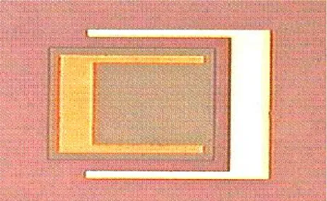
mesa sizes varying from 10µmx10µm (corresponding to 1.2 fF) to 300µmx300µm (corresponding to 1.5 pF). The devices also feature open optical windows in order to increase the incident light coupling into the device or the output light extraction from the device during operation. A micrograph of one of our fabricated near-UV QODs is shown in Fig. 2.
Fig. 2. Micrograph of a fabricated near-UV dual-operation quantum optoelectronic device.
Proc. of SPIE Vol. 6593 659324-2
C
0
(0 (0 E (0 C Ct 1 00 90 80 70 60 50 40 30 20 10 360 380 400wavelength(nm)
420 440 500 -4cc0o 30000-lccoo 0--/
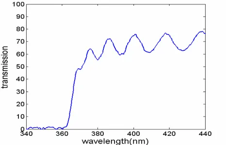
2cc 350 400 460 500 wavelength (nm) 3. RESULTSFollowing the epitaxial growth, we optically characterize the unprocessed wafer. We use a Xenon lamp (UV-Visible) to obtain the optical transmission spectrum. As depicted in Fig. 3, the optical transmission spectrum of our epitaxial design has an absorption band edge at 365 nm. Here we observe that the epitaxial structure is designed with the right band edge for operation in the near-UV range. In addition, the wafer transmits 80% of the incident light passing through. High transitivity of the wafer is particularly important for the optical extraction efficiency of our devices. Otherwise, in light emitting operation, light emitted from active region would be absorbed in the top and bottom epitaxial layers, which would decrease the output light power; and for the electroabsorption operation, the incident light would be blocked by the top (or the bottom) layers, which would increase the optical loss.
Fig. 3. Optical transmission spectrum of our near-UV dual-operation quantum optoelectronic device.
We also perform the photoluminescence characterization on the unprocessed wafer at room temperature by using a high power He-Cd laser with an excitation wavelength of 325 nm. When we pump the unprocessed wafer with He-Cd laser at 325 nm, we observe a photoluminescence (PL) peak at 370 nm with a full width at half maximum (FWHM) of 12 nm as shown in Fig. 4. This PL spectrum confirms that our epitaxial design features the proper concentration of In0.15Ga0.85N/
GaN quantum structures as targeted.
Fig. 4. Photoluminescence spectrum of our near-UV dual-operation quantum optoelectronic device.
Proc. of SPIE Vol. 6593 659324-3
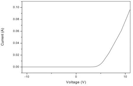
For the electrical characterization, current-voltage (I-V), electroabsorption (EA), electroluminescence (EL), and power-current (L-I) characterization are performed on the fabricated sample devices. We perform the I-V characterization by using a HP 4142 parameter analyzer. As shown in Fig. 5, the diode features a turn on voltage at ~5 V. Also its in-series parasitic resistance is measured to be ~70 Ω. Such low in-series parasitic resistance overcomes the local heating problem of the diode. -10 0 10 0.00 0.02 0.04 0.06 0.08 0.10 Curre n t (A) Voltage (V)
Fig. 5. Diode current-voltage characteristics of our near-UV dual-operation quantum optoelectronic device.
In reverse bias operation, we use a photocurrent measurement setup to obtain the optical absorption spectra by applying various levels of voltages. From the EA spectrum, the absorption coefficient is calculated by measuring the quantum efficiency from the spectral responsivity curve (taking Fresnel reflection into account) and assuming that all electron-hole pairs generated by the optical absorption process contribute to the photocurrent.
3700 380 390 400 410 420 430 1 2 3 4 5 6 7 8x 10 4 wavelength (nm) ab so rpt ion c oef fic ien t ( 1/ cm ) 0 V 1.5 V 3 V 4.5 V 6 V 7.5 V 9 V
Fig. 6. Optical absorption coefficient spectrum of our near-UV dual-operation quantum optoelectronic device.
Proc. of SPIE Vol. 6593 659324-4
2000 1500- 10005cc -2cc 350 400 460 500 wavelength (nm)
Fig. 6 shows the optical absorption coefficient spectrum of our device parameterized at reverse bias of 0 V to 9V (with 1.5 V increments). Fig. 7 shows the optical absorption coefficient change with respect to 0 V curve. Our quantum device exhibits a 14000 cm-1 absorption coefficient change at 385 nm with an applied reverse bias of 9 V in the spectral range
where it is highly transmissive, as also shown in the transmission spectrum in Fig. 3. In this measurement the range of dark current levels are a few nanoamperes. The level of optical absorption coefficient change that our device exhibits is very high. This shows that our near-UV quantum optoelectronic device, it operates as an electroabsorption modulator in the near-UV range when reverse bias applied to it.
385 390 395 400 405 410 415 -2000 0 2000 4000 6000 8000 10000 12000 14000 16000 wavelength (nm) abs or pt io n c oef fic ient c ha nge (1 /c m ) 1.5 V 3 V 4.5 V 6 V 7.5 V 9 V
Fig. 7. Spectral absorption coefficient change of our near-UV dual-operation quantum optoelectronic device with respect to the absorption curve at 0 V.
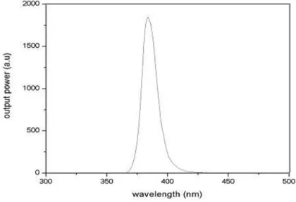
In forward bias operation, our quantum device features an EL peak at 383 nm with a FWHM of 20 nm as shown in Fig. 8. Here, the EL peak is observed to be sharp and in good agreement with the PL spectrum shown in Fig. 4. The EL peak in Fig. 8 is red-shifted with respect to the PL peak in Fig. 4 as expected. This EL peak verifies that, when forward bias applied to our near-UV quantum optoelectronic device, it operates as a light emitting diode in the near-UV range.
Fig. 8. Electroluminescence spectrum of our near-UV dual-operation quantum optoelectronic device at 20 mA.
Proc. of SPIE Vol. 6593 659324-5
IOU 90 Co 70
r
50 40 0 20 ID 300 400 500 600wa,ieIenth (rim)
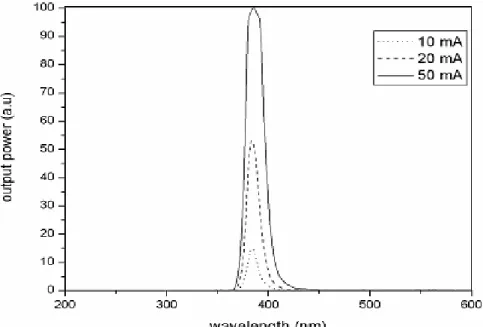
EL Fowe(tAI) 0. = = 0 = 0 = 9 0 0We also repeat the EA characterization at various current injection levels. We observe that as we increase the injected current level, the EA peak redshifts as shown in Fig. 9. The output power levels are normalized with respect to the output power at a current injection level of 50 mA.
Figure 9. Electroluminescence spectrum of near-UV dual-operation quantum optoelectronic device for varying current injection levels.
In addition, we show the optical output power characterization by coupling the light output from one side. Output power from bottom side is coupled to a powermeter, and it is measured to be larger than 0.35 mW for a current injection level of 50 mA as depicted in Fig. 10.
Figure 10. Light (power) vs. current relation of our near-UV dual-operation quantum optoelectronic device.
Proc. of SPIE Vol. 6593 659324-6
4. CONCLUSIONS
In this work we developed and demonstrated a near-UV dual-operation InGaN/GaN quantum optoelectronic device that operates as an electroabsorption modulator in reverse bias with a large absorption coefficient change of 14000 cm-1 at
385 nm for an applied bias change of 9 V, and as a light emitter in forward bias with >0.35 mW optical output power for a current injection of 50 mA at 383 nm. We reported for the first time dual operation of InGaN/GaN quantum structures in electroabsorption modulation and light emission in the near UV. In this paper, we presented the design, epitaxial growth, fabrication, and characterization of such dual-operation quantum optoelectronic devices.
5. ACKNOWLEDGEMENT
This work is supported by EU-PHOREMOST Network of Excellence 511616 and Marie Curie European Reintegration Grant MOON 021391 within the 6th European Community Framework Program and TUBITAK under the Project Nos. EEEAG 104E114, 106E020, 105E065, and 105E066. The authors also acknowledge additional support from the Turkish National Academy of Sciences Distinguished Young Scientist Award and TUBITAK Fellowship programs.
REFERENCES
1. S. P. Denbaars, “Gallium-Nitride-Based Materials for Blue to Ultraviolet Optoelectronics Devices”, Proceedings of
the IEEE, vol. 85, 1740-1749 (1997).
2. E. Fred Schubert, Light Emitting Diodes, Cambridge University Press, New York, 2006.
3. S. Nakamura, G. Fasol, S. J. Pearton, The Blue Laser Diode: The Complete Story, Springer, New York, 2000.
4. E. Sari, S. Nizamoglu, T. Ozel, and H. V. Demir, “Blue quantum electroabsorption modulators based on reversed quantum confined Stark effect with blue shift”, Applied Physics Letters, 90, 011101 (2007).
5. N. Biyikli, I. Kimukin, T. Tut, T. Kartaloglu, O. Aytur, and E. Ozbay, “High-speed characterization of solar blind AlGaN p-i-n photodiodes,” Semicond. Sci. Technol., vol. 19, pp. 1259–1262 (2004).
6. S. F. Chichibu, A. Shikanai, T. Deguchi, A. Setoguchi, R. Nakai, H. Nakanishi, K. Wada, S. P. DenBaars, T. Sota, and S. Nakamura, “Comparison of Optical Properties of GaN/AlGaN and InGaN/AlGaN Single Quantum Wells”, Jpn. J.
Appl. Phys. vol.39, 2417-2424 (2000).
7. D. M. Graham, A. Soltani-Vala, P. Dawson, and M. J. Godfrey, T. M. Smeeton, J. S. Barnard, M. J. Kappers, and C. J. Humphreys, E. J. Thrush, “Optical and microstructural studies of InGaN/GaN single-quantum-well structures”, J. Appl.
Phys., 97, 103508 (2005)
8. A. A. Allerman, M. H. Crawford, A. J. Fischer, K. H. A. Bogart, S. R. Lee, D. M. Follstaedt, P. P. Provencio, D. D. Koleske, “Growth and design of deep-UV (240-290 nm) light emitting diodes using AlGaN alloys”, J. Cryst. Growth, vol. 272, 227-241 (2004)
9. S. Nizamoglu, T. Ozel, E. Sari, and H. V. Demir, “White light generation using CdSe/ZnS core-shell nanocrystals hybridized with InGaN/GaN light emitting diodes”, Nanotechnology, 18, 065709 (2007).
10. Khan MA, Shatalov M, Maruska HP, Wang HM, Kuokstis E. “III-nitride UV devices”, Japanese Journal of Applied
Physics, Part 1-Regular Papers Short Notes & Review Papers, vol. 44, 10, 7191-7206 (2005).
11. I. Friel, C. Thomidis, and T. D. Moustakas, Journal of Applied Physics, 97, 123515 (2005).
12. P. Schlotter, J. Baur, Ch. Hielscher, M. Kunzer, H. Obloh, R. Schmidt, J. Schneider, “Fabrication and characterization of GaN/InGaN/AlGaN double heterostructure LEDs and their application in luminescence conversion LEDs (LUCOLEDs)” Materials Science and Engineering, B59, 390-394 (1999).
Proc. of SPIE Vol. 6593 659324-7