AKÜ FEMÜBİD 18 (2018) 011103 (441-450) AKU J. Sci. Eng. 18 (2018) 011103 (441-450)
DOİ: 10.5578/fmbd.67397
ARAŞTIRMA MAKALESİ
Ultrasonik Sprey Piroliz Tekniği ile Depolanan Bor-Katkılı CdS Filmlerinin
İncelenmesi
Murat Kellegöz
1, Hilal Çako
2, Seda Uzkalan
3, Salih Köse
11 Eskisehir Osmangazi University, Art&Science Faculty, Physics Department, Eskisehir. 2 Gazi University, Institute of Science, Ankara.
3 Dumlupinar University, Institute of Science, Kutahya.
e-posta: [email protected]
Geliş Tarihi:21.08.2017 ; Kabul Tarihi:17.08.2018
Anahtar kelimeler Yarı İletken Filmler; Bor Katkılı CdS Filmler;
Fotovoltaik Güneş Pili
Özet
Bor katkısının CdS filmlerin yapısal, yüzeysel, optik ve elektriksel özellikleri üzerindeki etkisi tartışılmıştır. Bor katkılı ince filmler, 300±5°C’de ultrasonik sprey piroliz tekniği ile kadmiyum klorid (CdCl2; 0.05M),
tiyüre (CS(NH2)2; 0.05M) ve borik asit (H3BO3; 0.05M) sulu çözeltisi kullanılarak payreks cam üzerine
çöktürülerek elde edilmişlerdir. Çöktürülen ince filmlerin optik, elektriksel, yapısal ve yüzey özellikleri UV spektrofotometre, dört prob tekniği, SEM, AFM ve XRD ile incelenmiştir. X-ışını kırınımı çalışması, filmlerin düşük boron katkıları için (011) düzleminde tercihli yönelmeye polikristalin olduğunu göstermektedir. Bununla birlikte, tercihli yönelme (002) olarak değişmiştir. Bor konsantrasyonu arttıkça tane boyu da artmıştır. Katkısız ve bor katkılı CdS ince filmlerin optik bant aralıkları 2.39-2.46 eV aralığında bulunmuştur. Tane boyutu dağılımı 30.8-115.4 nm aralığında elde edilmiştir.
Investigation of Boron-Doped CdS Films Deposited by Ultrasonic Spray
Pyrolysis Technique
Keywords Semiconductor Films; Boron Doped CdS Films; Photovoltaic Solar Cell AbstractThe influence of boron doping on the structural, surface, optical, and electrical properties of CdS films is discussed. Boron doped samples were deposited on pyrex glass slide using aqueous solution of cadmium chloride (CdCl2; 0.05 M), thiourea (CS(NH2)2; 0.05 M) and boric acid (H3BO3; 0.05 M) by
ultrasonic spray pyrolysis technique at 300±5°C. Optical, electrical, structural and surface properties of the deposited thin films were studied by UV spectrophotometer, four probe technique, SEM, AFM, and XRD. XRD study shows that films are polycrystalline with preferred orientation through (011) plane for low boron in corporations. However, preferential orientation changed to (002). The grain size has increased with increasing boron concentration. The optical band gap of the undoped and boron doped CdS samples were found in the range of 2.39-2.46 eV. Grain size distribution is obtained in the range of 30.8-115.4 nm.
© Afyon Kocatepe Üniversitesi
1. Introduction
Recently, there has been increasing interest in research on II-VI materials because these materials have found great use in the electronic-devices industries. CdS thin film is the generally used window layer for the high efficiency CdTe, and CuInSe2 (CIS) polycrystalline thin film solar cells
(Lee et al. 2003). The CdS samples deposited by ultrasonic spray pyrolysis (USP) technique is stoichiometric in composition and the optical,
electrical, surface morphology and crystal structure of the CdS film is readily controllable. Recently, it is reported that the boron-doped CdS samples can be deposited by USP technique using boric acid (H3BO3) as a dopant. It was found that
boron-doping is an alternative for decreasing the resistivity of CdS films (Ahmed & Dakhel 2012). CdS film is a II-VI compound polycrystalline semiconductor with a direct optical band gap of Eg=2.42 eV at room temperature. CdS thin films
Afyon Kocatepe Üniversitesi Fen ve Mühendislik Bilimleri Dergisi
442 were worked for different applications as
photovoltaic solar cells (PV), optical detectors and some other optoelectronics devices (Novruzov et al. 2013).
CdS samples grow usually in the structure of wurtzite without external doping; they show n-type electrical conductivity which might be due to native defects or sulfur vacancies and Cd interstitials. Because of the wide and direct band gap transition, high refractive index (n=2.5) and high electron affinity properties, CdS has been most generally used as window material in high efficiency thin films solar cells based upon CdTe, Cu(In,Ga)Se2 and
Cu2S (Chu and Chu 1995, Contreas et al. 1999,
Jayakrishan et al. 1996, Khallaf et al. 2009, Wu et al. 2001).
Today, it is known pollutions in semiconductors cause some important changes in their optical, electrical, surface and structural properties. The boron-doped CdS can enhance its electrical, optical and magnetic properties. Boron is an important element that having an ionic radius of 0.20 Å. While it is smaller than Cd+2 (0.97 Å), B+3 ions can
very easily penetrate into CdS crystal lattice replacing Cd+2 ions to improve their physical
properties. Boron-doped CdS is a promising mater for some optoelectronic applications, such as LED and solar cells. USP method is authenticated to be an effective one for preparing CdS samples with large-area uniformity and strong adhesion. Therefore, CdS thin films containing inorganic/organic heterojunction solar cells have been attracting attention in the field.
The spray pyrolysis technique is an easy way in which an ionic solution –including the constituent elements of a compound in the form of soluble salts– is sprayed onto preheated substrates using a stream of dry and clean air (Ashour, 2003). Spray pyrolysis is a low-cost technique generally used to deposit CdS samples. This technique used for the fabrication of samples of simple oxides, mixed oxides, metallic spinal type oxides group I-VI, II-VI, III-VI, and IV-VI (Patil, 1999). In virtually all cases reported in the literature, one impurity at a time such as aluminum, chlorine, fluorine, indium, or copper is used as a dopant to control the electrical
behavior of a semiconductor (Akintude, 2000). CdS exist in two kind of crystalline: the hexagonal (wurtzite) and the cubic (zinc blende) phase (Britt and Ferekides 1993, Feitosa et al. 2004).
In this work, boron-doped CdS samples were sprayed by USP technique, followed by doping at different boron concentrations in mixed CdCl2 and
thiourea starting solutions. The effects of doping on optical, electrical, structural (XRD) and surface morphologies (SEM, AFM, OPM) were investigated.
2. Experimental Procedures
Boron-doped CdS samples were deposited onto pyrex glass substrates by using ultrasonic spray pyrolysis (USP) technique from aqueous solution mixtures of equimolar cadmium chloride (CdCl2 :
0.05M), thiourea (CS(NH2)2 : 0.05M) and boric acid
(B3HO3 : 0.05M) in deionized water. Volumes of
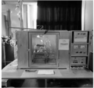
starting solutions are given in Table 1. The experimental set-up we used for the process is seen in Figure 1. The pH of the mixture was measured to be 7.6 at room temperature and the spraying velocity was 5 ml/min. Prior use, the glass slides were soaked to clean in deionized water about 30 min, and they were left to air dry in the spraying chamber. The atomization of the starting solutions into a spray of droplets is controlled by ultrasonic spray nozzle, with the aid of compressed air (~1 bar) as a carrier gas. Totally, 100 ml of solution has been sprayed for each film. The thicknesses of the samples were measured by using an elcometer (Elcometer, 345N, 0-1000 µm) with an experimental error of ±4%.
443 Figure 1. Experimental set-up.
Three solutions were mixed over a magnetic heater for 30 min with continuous stirring. The spraying chamber was purged by the snail fan during deposition. After the deposition, films were left inside the chamber for 12-24 hours to cool down to room temperature. Since variations in spraying parameters can have a notable effect on the properties of the deposited films, standard spray conditions must be carefully specified.
Table 1. Contents of the starting total solutions (ml) Material CdCL2 (ml) CS(NH2)2 (ml) B3HO3 (ml) Starting total solution (ml) CdS 50 50 0 100 B1 45 50 5 100 B2 40 50 10 100 B3 35 50 15 100 B4 30 50 20 100 B5 25 50 25 100 3. Measuring Instruments
We have characterized the surface morphology by using SEM, AFM and optical microscopy techniques. The parameters of the films were determined using XRD technique. The XRD patterns were obtained with Panalythical Emperyan 45 kV/40 mA, XRD using a Cu-Kα radiation source
(λ=1.54018 Å). The absorbance and transmission spectra of boron-doped CdS samples were recorded by using Shimadzu UV-VIS 2550 model (0-60oC) spectrophotometer (double beam). The
optical band gaps of the samples were determined
by using the optical method. The electrical properties; resistivity and electrical conductivity type were studied by the four-probe (Keithley 2601A System Sourcemetre, Lucas Labs Pro4) and hot-probe techniques, respectively.
4. Results and Discussion
4.1. XRD Analyzes
To investigate the preferential orientation and the crystallinity of undoped and boron-doped CdS samples, XRD measurements were performed over a diffraction angle range of 20o to 60o. The XRD
patterns of the samples are given in Figure 2. The x-ray diffraction works remarked that all the samples were polycrystalline with CdS, B2S3, and B8S16
phases. For low boron rates, the spectrum illustrated a powerful peak oriented at (011) direction. As increasing the boron doping fraction, especially for samples B3, B4 and B5, (002) peak dominate the structure. Thus, we can say that boron incorporation rate has an important effect on the preferential orientation of CdS films. In addition, higher amounts of boron incorporation caused an augmentation in d values of CdS films. The radius of the B+3 (0.24 Å) is much smaller than
Cd+2 (0.97 Å) ion. So, the B+3 ions can be displaced
by Cd ions in the crystal structure of boron-doped CdS. This may cause the change in lattice constant and the position of the peaks. The first three intense peaks located between 25°-29° angles, corresponds to hexagonal CdS. By the incorporation of boron into the CdS structure, B2S3
and B6S8 phases were formed in the monoclinic
structures. As can be seen from Figure 2, no other phases corresponding to a metal (such as Cd, etc.) were detected, and the hexagonal structure of CdS film did not change with increasing boron content. The grain size values and the half peak widths for the orientations of undoped and boron doped CdS samples were computed using Scherrer-Debye formula (Ashour, 2003; Cullity, 1979)
𝐷 = 0.9𝜆 𝛽 cos 𝜃⁄ (1) where β is the half peak width as radian of the maximum intensity peak, D is the particle size, θ is
444 the Bragg angle and λ is the X-ray wavelength. Also,
δ is the dislocation density of the samples which is given by Williamson and Smallman’s relation (Park, 2010). These values are given in Table 2.
𝛿 = 1 𝐷⁄ 2 (2)
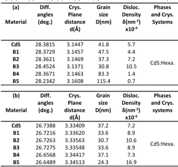
Table 2. Crystal parameters obtained from XRD data for (a) (011) peak, (b) (002) peak; (Ref.code:98-015-4186)
(a) Material Diff. angles (deg.) Crys. Plane distance d(Å) Grain size D(nm) Disloc. Density δ(nm-2) x10-9 Phases and Crys. Systems CdS 28.3815 3.1447 41.8 5.7 CdS:Hexa. B1 28.3729 3.1457 47.5 4.4 B2 28.3621 3.1469 37.3 7.2 B3 28.4524 3.1371 30.8 10.5 B4 28.3671 3.1463 83.3 1.4 B5 28.2342 3.1608 115.4 0.7 (b) Material Diff. angles (deg.) Crys. Plane distance d(Å) Grain size D(nm) Disloc. Density δ(nm-2) x10-9 Phases and Crys. systems CdS 26.7388 3.33409 37.2 7.2 CdS:Hexa. B1 26.7216 3.33620 33.6 8.9 B2 26.7263 3.33563 30.7 10.6 B3 26.7275 3.33548 33.6 8.9 B4 26.6568 3.34417 37.1 7.3 B5 26.6489 3.34513 24.3 16.9
Figure 2. XRD patterns of undoped and boron doped CdS samples.
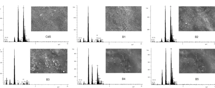
4.2. SEM Morphologies and EDS Analyzes
SEM images and EDS analysis of the obtained undoped and boron doped CdS films were taken from Zeiss Supra 40 VP scanning electron microscope. Our main goal here is to examine the change of images on the surfaces of films and microanalysis by EDS. Figure 3 shows SEM images and EDS spectra of undoped and boron doped-CdS thin films. The surface of the undoped and boron doped samples were examined by SEM. The morphologies of CdS samples vary considerably with boron concentration. In addition, it also designated that the islands with various sizes, such as matrix and white regions were seen on the surfaces of the samples and the dispersion of the islands is not homogenous in all samples. Therewithal, there exist intensive white islands on the surfaces of boron doped samples. The size of these area augment depends on boron
445 concentration. In addition, it is hard to fabricate
smooth and homogeneous samples by USP method.
EDS spectra of the thin films deposited at various boron concentrations were obtained to see whether Cd and S elements are present in the related samples or not. The EDS spectra of the thin films are shown in Figure 3. The atomic number of boron atom is five, so it does not appear in EDS spectra. Elemental weights in starting solutions and deposited solid films are not absolutely the same. Table 3. EDS analysis
Material Matrix Mole.Conc.(%) White islands Mole.Conc.(%) Cd S Cd/S Cd S Cd/S CdS 56.252 43.748 1.285 57.629 42.371 1.360 B1 57.934 42.066 1.377 57.337 42.663 1.344 B2 57.156 43.844 1.304 57.729 42.271 1.366 B3 58.808 41.192 1.428 56.176 43.824 1.282 B4 55.567 44.433 1.251 56.117 43.883 1.279 B5 55.193 44.807 1.232 55.104 44.896 1.227
As shown in Table 3 the concentration of cadmium in both matrix and white islands is greater than that of sulfur. The Cd/S ratio decreases by each increase of the doping concentration of boron. It is clear that boron incorporation has an effect on Cd/S ratio. For low rates of boron incorporation the Cd/S ratio increases. But, Cd/S ratio tends to decrease for higher boron concentration. This decrease of Cd amount refers a substitution of Cd atoms by boron atoms.
4.3. AFM studies
The 3-dimensional (3D) image (5x5µm2) obtained
from AFM for undoped and boron doped CdS samples are shown in Figure 4. As can be seen that the surface of all the undoped and boron doped CdS samples is composed of dense grains having well-defined grain boundaries. The root mean square (RMS) roughness (Rq) of the samples is calculated using the equipment’s software routine.
Figure 3. SEM image and EDS spectrum of the films.
These values together with average roughness values (Ra) are given in Table 4. The roughness of samples plays a vital role in developing optical coatings especially in the UV-VIS region (Kalem et al. 2010, Phatak and Lai 1992). The effect of the increase of boron on surface morphology of the samples has been seen. It is obvious that a granular structure without cracks could be seen for all samples. The images indicate that surfaces are non-homogeneous and densely packed. Increasing
in boron concentration in total starting solution volume, the films have a little smoother surface with irregular shape and larger size grains.
Table 4. Roughness values of undoped and boron-doped CdS films Material Rq(nm) Ra(nm) CdS 15 12 B1 6 5 B2 9 7 B3 24 17
446
B4 104 65
B5 154 121
447 Figure 5. The optic microscope image of all films.
4.4. Optical microscope images
Obtained boron-doped CdS films were examined at x100 magnification on a camera (Clemex) optical microscope (Nikon Eclipse LV150N) which are shown in Figure 5, and the changes in their surface were investigated. In general, the discoloration of the surface from optical surface images of semiconductor films is closely related to the intensities of the crystal defects in the surface. This color change affects the species and additive concentrations of the elements incorporated into the main sample. CdS is a light-sensitive material. These light-affected samples have their own surface colors. For this reason, there is a color change on the surfaces when foreign elements added. This color change affects the physical properties of the sample, especially the reflection or absorption of the light coming from the surface, in positive or negative directions. CdS films have greenish islands on their surface. We are not entirely sure, but we can say that the color changes on the surface are caused by Cd+2 and S-2 ions
which have not bonded on the surface. On the other hand, additive elements may exhibit such behavior. Not enough research has been done in this regard. When viewed from the surface of the CdS samples with a naked eye, the orange yellow
color is noticed. However, when examined under an optical microscope, it appears that there are green and red islands on their surface. The black islands appearing on the surfaces of the resulting boron-doped films are caused by agglomerations due to large droplets during spraying procedure. Because of this, due to the partial deterioration of the mouth geometry of the spray head, the films cannot hold on to the bottom due to the sudden shock of large droplets reaching to the bottom. Similar images are also available in SEM images. In optical microscope images, the reason for the x100 magnifications selection is that the black islands are seen more clearly in this magnification. The high density of these islands affects the electrical properties (electrical resistivity or conductivities) of the films negatively. In the regions shown by the blue arrow, a film was not formed. Such occurrences are caused by weakly deposited agglomerates on the surface and there is no crystal formation.
The forbidden energy range of CdS films in greenockite construction is 2.42 eV at room temperature, which can cause discoloration due to this broad forbidden energy range, reddish, yellow, green and orange colors on optical microscope surface images (Nassau, 2001). There are some
448 black islands on the surface of undoped and
boron-doped CdS films.
4.5. Some optical properties
The transmission and absorption spectra of all the samples were measured in the wavelength range between 300 and 600 nm at room temperature. The boron doped CdS samples illustrated a high absorption coefficient, α higher than 104 cm-1
above fundamental absorption. The optical band gap of the samples was designated from (αhν)2
versus (hν) plots which are shown in Figure 6. Maximum transmittance value of the sample B4 is 60% and this value decreases by boron concentration. The minimum transmittance value for B3 is 30%. Surface roughness, grain boundaries, and morphology may affect the intensity of the reflected light. The band gap variation of all films is given as (Hankove and Chate 2009; Pankove, 1971).
(𝛼ℎ𝜈) = 𝐴(ℎ𝜈 − 𝐸𝑔)𝑛 (4)
For n=1/2 (for allowed direct optic band gap semiconductor), Eg is the optical band gap and hν is
incident photon energy, and as a function of hν, and extrapolating the linear portion of the curve to (αhν)2=0 as shown in Figure 6. The obtained value
for the optical direct band gap is 2.39-2.46eV, where A is a constant, and n is a constant too which is equal to 1/2 for a direct-allowed band gap semiconductor and 2 for an indirect-allowed band gap (Pankove, 1971).
Transmittance and absorbance measurement of doped samples were performed to investigate the effect of boron doping on some optical properties and optical band gap of CdS films. Figure 6 shows the effect of boron ion concentration on the transmission spectra for all of the films at the range 300-600 nm.
Figure 6. (αhυ)2 versus (hυ) changes, absorbance and transmission spectra of the films.
4.6. Electrical resistivity
The electrical resistivity of the thin films was measured by using four probe techniques. The resistivity of the undoped and boron doped CdS thin films ranged between 2.77×10⁶ Ωcm and
7.28×10⁶ Ωcm. The type of conductivity of the films
was designated by hot probe technique (Seeger, 1982). All films illustrated n-type conductivity. The
addition of boron into the CdS films did not make a noticeable vary in the electrical conductivity of the CdS samples.
5. Conclusion
Undoped and boron doped CdS samples were deposited by USP technique using solutions of CdCl2, H3BO3, and CS(NH2)2. The films were sprayed
Investigation of Boron-Doped CdS Films Deposited by Ultrasonic Spray Pyrolysis Technique, Kellegöz vd.
449 onto non-coated microscope glass substrates, and
substrates are kept at the selected temperature of 300±5ᵒC. The optical band gaps of the samples were calculated in the range of 2.39-2.46 eV, depending on the boron doping concentration. In the visible range, the optical transmittance of CdS samples depends on the boron doping concentration.
The electrical resistivity was found to be in the range 2.77x10⁶-7.28x10⁶ Ωcm varying with boron
doping concentration in air ambient at room temperature. Undoped and boron doped CdS samples were shown a high resistivity approaching ~106 Ωm. But the resistivity of the films due to
boron doping was not investigated thoroughly. Hot probe experiments showed that undoped and boron doped films are having n-type electrical conductivity.
The crystal structures of undoped CdS films were hexagonal phases and boron doped CdS samples have both hexagonal and monoclinic phases with a preferential orientation changing from (011) to (002) for high concentrations. The grain size of undoped and boron doped CdS samples were found to be between 30.8-115.4 nm.
AFM images were to examine the 3-D surface topology and surface roughness values of the films. The Rq values changed between 6-154 nm. Surface properties and elemental analysis of all films have been investigated by scanning electron microscopy (SEM) and energy dispersive x-ray spectroscopy (EDS). The properties of surface color changing have been studied by using the optic microscope. We conclude that low amounts of boron doping into CdS may give better results. The undoped and boron doped surfaces were observed to resemble each other and they had a smooth and nearly featureless appearance. The surface roughness of CdS films increased for high rates of boron doping. This increase can be attributed to the crystal defects. In the EDS spectra of boron doped CdS samples, the peak was belonging to boron atom that did not appear due to the fact that it had five atomic numbers. However, decreasing CD/S ratio refers the substitution of Cd atoms by boron
atoms. But XRD, SEM, AFM and OPM
measurements indicated that the boron doping
into CdS affected the optical, electrical, structural and surface properties. These results propose that the technique of ultrasonic spray pyrolysis for the deposition of boron doped CdS samples should be further investigated for application towards the fabricating of photovoltaic solar cells.
Acknowledgment
Financial support from Eskisehir Osmangazi University Research Fund (Project No: 2013/19031) is gratefully acknowledged.
References
Ahmed, H.H. and Dakhel, A.B. 2012. The Effect of the Solution Concentration on Structural and Optical Properties CdS Thin Films Prepared by Chemical Bath Deposition Technique. International Journal of
Recent Research and Review, IV, 8-13.
Akintunde, J.A., 2000. Dual impurity doping of buffer solution grown cadmium sulphide thin films: electrical and optical properties. Journal of Materials
Science: Materials in Electronics, 11, 503-508.
Ashour, A., 2003. Physical properties of spray pyrolysed CdS thin films. Turkish Journal of Physics, 27, 551-558.
Britt, J. and Ferekides, C., 1993. Thin-Film Cds/Cdte Solar-Cell with 15.8 Percent Efficiency. Applied
Physics Letters, 62, 2851-2852.
Chu, T.L. and Chu, S.S., 1995. Thin film II-VI photovoltaics. Solid-State Electronics, 38, 533-549. Contreas, M., Egaas, B., Ramanthan, K., Hiltner, J.,
Swartzlander, A., Hasoon, F. and Noufi, R., 1999. Progress toward 20% efficiency in Cu (In, Ga) Se2 polycrystalline thin‐film solar cells. Progress in
Photovoltaics: Research and applications, 7/4,
311-316.
Cullity B., 1978. Elements of X- Ray Diffraction. Addison-Wesley, 81-106.
Feitosa, A.V., Miranda, M.A., Sasaki, J.M. and Araujo-Silva, M.A., 2004. A new route for preparing CdS thin films by chemical bath deposition using EDTA as ligand. Brazilian Journal of Physics, 34, 656-658. Hankare, P.P., Chate, P.A. and Sathe, D.J., 2009. CdS thin
film: Synthesis and characterization. Solid State
Investigation of Boron-Doped CdS Films Deposited by Ultrasonic Spray Pyrolysis Technique, Kellegöz vd.
450
Jayakrishnan, R., Nair, K.P., Kuruvilla, B.A., Kulkarni, S.K. and Pandey, R.K., 1996. Characterization and photovoltaic device application of dip-coated and rapid thermal annealed CdS films. Journal of
Materials Science: Materials in Electronics, 7/3,
193-199.
Kalem, S., Arthursson, O. and Romandic, I., 2010. Formation of germanates on germanium by chemical vapor treatment. Thin Solid Films, 518, 2377-2380. Khallaf, H., Chai, G., Lupan, O., Chow, L., Heinrich, H.,
Park, S. and Schutle, A., 2009. In-situ boron doping of chemical-bath deposited CdS thin films. Physica
Status Solidi a-Applications and Materials Science,
206/2, 256-262.
Lee, J.H., Yi, J.S., Yang, K.J., Park, J.H., and Oh, R.D., 2003. Electrical and optical properties of boron doped CdS thin films prepared by chemical bath deposition. Thin
Solid Films, 344, 431-432.
Nassau,K., 2001. The Physics and Chemistry of Color: The Fifteen Causes of Color. Wiley Interscience, 157-185.
Novruzov, V.D., Keskenler, E.F., Tomakin, M., Kahraman S. and Gorur, O., 2013. Effects of ultraviolet light on B-doped CdS thin films prepared by spray pyrolysis method using perfume atomizer. Applied Surface
Science, 280, 318-324.
Pankove, J.I., 1971. Optical Processes in Semiconductors. Prendice-Hall, 34-86.
Park, W.D., 2010. Photoluminescence of nanocrystalline CdS thin films prepared by chemical bath deposition.
Transactions on Electrical and Electronic Materials,
11/4, 170-173.
Patil, S.P., 1999. Versatility of chemical spray pyrolysis technique. Material Chemistry and Physics, 59, 185-198.
Phatak, G. and Lai, R., 1992. Structural and electrical-properties of cadmium-oxide films deposited by the activated reactive evaporation technique. Thin Solid
Films, 209/2, 240-249.
Seeger, K., 1982. Semiconductor Physics. Springer, 83. Wu, X., Keane, J.C., Dhere,R.G., Dehart, D., Albin, D.S.,
Duda, A., Gessert, T.A., Asher, A., Levi, D. and Sheldon, P., 2001. 16.5% Efficient CdS/CdTe Polycrystalline Thin-Film Solar Cell. In Proceedings of