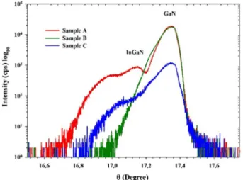
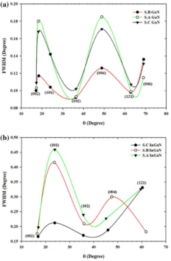
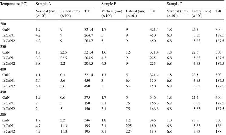
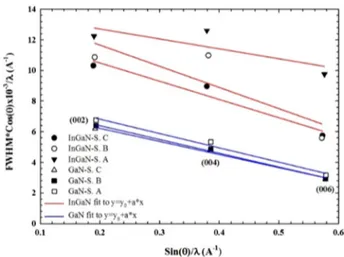
Investigation of structural, optical and morphological properties of InGaN/GaN structure
Tam metin
Şekil
Benzer Belgeler
Araºtýrmanýn üçüncü yýlýnda ise, 5 kg/da azot uygulamas ý ve 5 kg/da fosfor ile birlikte uygulanan 10 kg/da azot diðer familya bitkilerinin mera verimine kat
Spike analyses for ISI tuning. The first hypothesis we tested was that the ISI/speed tuning of neuronal responses in area MT reflected selectivity for perceived ISI/speed as
The focusing behavior of the designed device was analyzed, both theoreti- cally and experimentally, and indicated that a small number of columns are sufficient to focus a spatially
In order to respond to the specific needs of a community that is ever-changing and diversifying, new associations such as the Turkish Society of Canada founded in 2006 or the
Keçebaş, Alkan ve Bayhan (2011) yaptıkları çalışmada, P 1 -P 2 maliyet analiz yöntemi ile yaşam döngüsü maliyet analizine bağlı olarak Afyonkarahisar ili için
Mutations in the VLDRL gene have been well described in both animal models and in humans and underscore its importance in cerebellogenesis. While mutations in Reln in the mouse
Abbreviations: CTS, cell-type-specific; DAWN, detecting association with networks; CTS-DAWN genes, genes identified by DAWN in specific cell types; ExN, excitatory neurons;
3.4 Saturation (RF pump on) and subsequent relaxation (RF pump off) of spin-3/2 system starting from the thermal state with quadrupolar
