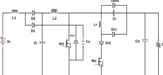
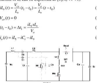
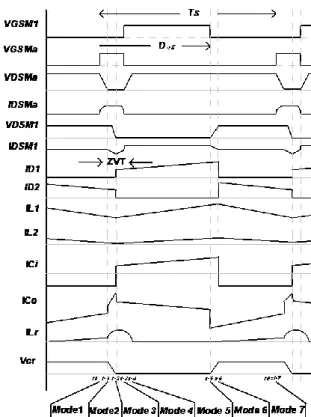
Analysis of a soft switched dual-boost converter
Tam metin
Şekil
Benzer Belgeler
Application of only integrated multipoint converter in speed control of switched reluctance motor drive cause higher voltage stress on the switches and capacitors due to the
Design, modeling, and implementation of Boost Converter with state feedback controller using pole placement technique and Linear Quadratic Optimal Regulator (LQR)
Furthermore, the proposed model can be useful to achieve input and output impedances, inductor current variations, and converter transfer functions to develop a robust
Beşinci Halife Harfin- ür-Reşid’in üç oğlu, Emin, Me’mun, Mu’tasım ki üçü de sonra sıraları gelince arka arkaya halife olacak lar, hepsi Türk
Sille Çayı Havzası ve yakın çevresindeki volkanitlerin, pre-volkanik araziyi oluşturan formasyonlarla, Miosen göl tabakalarıyla ve volkanitleri fosilize eden örtü
İsmet P aşa, hayatına o kadar ağır bir damga vurmuştu ki, onu an latmaktan bir türlü kendisine gele memişti sıra.... Çok nadiren söz ederdi kendi
Kısa sürede başarılı bir seramik sanatçısı olarak tanınan Füreya, birçok bina için duvar panoları hazırladı.. Daha sonra hayvan biçimli plastikler, vazo
büyük katkıda bulunmuş olan Süreyya Ağa oğlu, ayrıca pek çok dernekte de kurucu üye ya da üye olarak görev almış, yurtiçinde ve yurtdışında pek çok
