PROCEEDINGS OF SPIE
SPIEDigitalLibrary.org/conference-proceedings-of-spieBroadband absorption enhancement
in an uncooled microbolometer
infrared detector
Basak Kebapci
Ozgecan Dervisoglu
Enes Battal
Ali Kemal Okyay
Tayfun Akin
Broadband absorption enhancement in an uncooled microbolometer
infrared detector
Basak Kebapci
1, Ozgecan Dervisoglu
1, Enes Battal
2, 3, Ali Kemal Okyay
2, 3, and Tayfun Akin
1, 4 1METU-MEMS Research and Application Center, Middle East Technical Univ., Ankara, Turkey
2
Dept. of Electrical and Electronics Engineering, Bilkent University, Ankara, Turkey
3UNAM-National Nanotechnology Research Center and Institute of Materials Science and
Nanotechnology, Bilkent University, Ankara, Turkey
4
Dept. of Electrical and Electronics Engineering, Middle East Technical Univ., Ankara, Turkey
ABSTRACT
This paper introduces a method for a broadband absorption enhancement in the LWIR range (8-12 µm), in single layer microbolometer pixels with 35 μm pitch. For the first time in the literature, this study introduces a very simple and low cost approach to enhance the absorption by embedding plasmonic structures at the same level as the already existing metallic layer of a microbolometer pixel. The metal layer comprises the electrode and the arm structures on the body. Even though the periodicity of the plasmonic structures is slightly disturbed by the placement of the electrodes and the connecting metal, the metal arms and the electrodes compensate for the lack of the periodicity contributing to the resonance by their coupling with the individual plasmonic resonators. Various plasmonic structures are designed with FDTD simulations. Individual, plasmonically modified microbolometer pixels are fabricated, and an increase in the
average absorption due to surface plasmon excitation at Au/Si3N4 interfaces is observed. Plasmonic structures increase
the average absorptionfrom 78% to 82% and result in an overall enhancement of 5.1%. A good agreement between the
simulation and the FTIR measurement results are obtained within the LWIR range. This work paves the way for integration of the plasmonic structures within conventional microbolometer devices for performance enhancement without introducing additional costs.
Keywords: Microbolometers, absorption enhancement, LWIR, broadband, surface plasmons.
1. INTRODUCTION
In the long-wave infrared (LWIR) range, the photon detectors appeal with their high speed and high responsivity however a cooling system is mandatory to achieve low noise and ultimate sensitivity, which makes them very expensive products. Microbolometer-based uncooled imagers, on the other hand, offer low cost, light weight and easy-to-integrate solutions.
The figures of merit identifying the performance of an uncooled infrared detector are mainly; temperature sensitivity, thermal conductance, responsivity, noise equivalent power (NEP), noise equivalent temperature difference (NETD), and detectivity [1]. Absorption is directly related to responsivity, NEP, NETD, and detectivity of the infrared detectors. Therefore, an increase in the absorption also improves the performance of the microbolometer.
Many methods have been investigated to increase the absorption of an infrared detector so far, including antireflection coatings [2, 3], impedance matching [4], surface texturing [5], and resonant photonic structures [6] or plasmonics. Plasmonics is an emerging field that has found wide-spread applications such as photovoltaics [7], photothermal cancer therapy [8], single molecule biosensing [9], and infrared detectors [10]. A common approach to induce plasmonic effects is to employ patterned micro/nano metallic structure within the vicinity of a dielectric interface. Electromagnetic waves cause collectively oscillations of free electrons within the metal and form the guided surface waves called surface plasmon polaritons (SPPs). SPPs can result in immense field confinement, which is used for absorption enhancement [11].
This paper studies the design and integration of plasmonic structures into a complete microbolometer pixel for improved absorption in the 8-12 µm spectral range. We have previously shown that plasmonic structures can be utilized for strong absorption in the infrared [12] and further demonstrated that plasmonic features can be utilized for strong absorption
Si3N4 Ti Au NiCr Polyimide (PI) Active Material
enhancement in the bolometric structures [13]. Here, we introduce plasmonic structures into a rather more complex microbolometer pixel which includes a resistive material, metal electrodes providing electrical contacts between the read-out circuitry and the resistive layer through the support arms, and a very thin metal film that is used as the absorber
layer. We fabricated the microbolometers with integrated co-centric square ring plasmonic features with different
periodicity and feature sizes. We also spanned the structure parameters investigated in our previous study for comparison. The integration of plasmonic features is carried out without introducing any additional fabrication steps, avoiding any increase in the complexity or cost. Section 2 presents the fabrication of the complete microbolometer pixel with the plasmonic features. Section 3 gives the comparison of the simulation and the measurement results of the absorption within the 8-12 µm range. Finally, Section 4 summarizes the achievements obtained by using the co-centric plasmonic features.
2. FABRICATION OF THE MICROBOLOMETER PIXEL
In the fabricated microbolometers (35 µm pixel-pitch), silicon nitride dielectric film is chosen as the structural layer due to its good absorption characteristics in the LWIR range. On the other hand, planar type resistors are chosen due to their simple process steps. On top of the microbolometer structure, nichrome (NiCr) is used as an additional absorber layer.
Figure 1 depicts the process steps done for the formation of the microbolometer pixels
.
Figure 1. 3D views of the fabrication steps of the 35 µm pitch microbolometer pixel decorated with plasmonic features. (a) back reflector of the pixel (Ti/Au), (b) sacrificial layer (polyimide) coating and opening at the contacts, (c) structural layer (Si3N4) deposition and the contact openings with RIE, (d) arm (Ti) formation, (e) deposition and patterning of the electrodes
including the plasmonic structures (Cr/Au), (f) deposition and patterning of the active material layer, (g) deposition and patterning of the protection layer (Si3N4) for the active material, (h) deposition of the second structural layer (Si3N4),
deposition and patterning of the absorber layer (NiCr), followed by the patterning of the whole structural layer for the pixel formation, (i) sacrificial layer (polyimide) is removed; suspended view of the pixel.
(a) (b) (c)
(i)
(d) (e) (f) (g) (h) (i)
(b)
(a) (a)
The fabricated microbolometer pixels are formed with 8 different photolithography masks. The first layer is the mirror (back reflector) layer that reflects the light back inside the microbolometer’s body. The mirror layer consists of titanium
and gold bilayer (20 nm/70 nm). As the 2nd step, 2 µm thick polyimide is coated as the sacrificial layer, and the contacts
are opened by the polyimide RIE. On the 3rd step, the structural layer, silicon nitride thin film (0.2 µm) is deposited on
top of the PI layer, by the PECVD; the contact holes are opened again by the RIE, with a smaller mask size than the PI openings. On top of the first structural layer, 60 nm thick titanium arms are formed. As the most crucial step, chromium and gold bilayer is deposited (20 nm/70 nm); the electrodes and the plasmonic features are formed by wet etching with a single mask. After this step, the active material of the microbolometer is deposited and patterned. Right after that, to protect the active material, silicon nitride (0.1 µm) is deposited and patterned with the same mask used for the active material. Again, silicon nitride, second structural layer (0.2 µm), is deposited on top of the layers. On the top, the absorber layer, nichrome thin film (5 nm), is sputtered and patterned. 0.4 µm silicon nitride structural layer is etched in the RIE, and the structural layer formation is finished. Finally, the polyimide, sacrificial layer is released in the oxygen plasma.
3. SIMULATION AND MEASUREMENT COMPARISON
There are three different plasmonic features chosen for this study. Parametric optimization for all of the three different plasmonic features is performed considering infinitely periodic unit cells. However, the simulations are repeated on the whole pixel body to see the effect of the metal electrodes and the arms located in the middle of the plasmonic features. All numerical simulations are performed using FDTD Solutions by Lumerical Inc. The material database of the Lumerical is used during the simulations (except for the dielectric properties of silicon nitride and the active material). The dielectric properties of silicon nitride (deposited in the PECVD system) between 6-16 µm wavelength were given
previously [13]. The absorption is calculated from the reflected power, Preflected, as 1- Preflected.
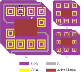
Figure 2 gives the size and the periodicity parameters with the top view of the designed pixel bodies corresponding three plasmonic structures, namely, S-1, S-2 and S-3 respectively. However, these parameters are changed after the wet etching process of the Cr/Au (electrode-plasmonic) layer. The process imperfections as the undercut problems in the
plasmonic features are solved by importing the SEM images of the fabricated pixels to the simulation area (see Figure 3.). Due to computational limits, pixel arms are not included into the simulations, only the pixel bodies are taken
into account.
Figure 2. The views of the designed pixel bodies with different plasmonic features. The pixels with plasmonic features are named as S-1, S-2, and S-3. Periodicity, length of the outer and the inner rings are symbolized as P, L1 and L2 respectively, and shown on the S-1, in (a). The width of the outer and inner square rings is: 0.5µm. (a) S-1: P = 5.4 µm, L1 = 4.5 µm, and L2 = 2.5 µm. (b) S-2: P = 8.1 µm, L1 = 4.5 µm, and L2 = 1.8 µm. (c) S-3: P = 8 µm, L1 = 4 µm, and L2 = 1.6 µm.
mm 11a JUL 8/21/2013 10,0kV LEI SM n3 10m 12:12:44 PM 10p1 !¢TUM>NS 3/10/20:4 SEM MD 11a 4:30:33 P:-t
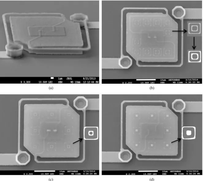
Figure 3 shows the scanning electron microscope (SEM) images of the suspended microbolometer pixels without any plasmonic structures (reference) and with the three different co-centric designs. The plasmonic structures’ SEM images are processed to be able to insert the SEM images into the Lumerical design environment successfully. These images are formed from the SEM pictures taken after the patterning of the plasmonic features (Figure 1 (e)), as shown on the S-1 pixel’s SEM image, in Figure 3 (b).
Figure 3. The SEM images of the 35 µm pixel-pitch, single layer microbolometer structures, which are all suspended.
Nearby the plasmonically enhanced pixels, the processed images of the plasmonic structures are given. (a) The reference pixel (without any plasmonic features), (b) Top view of the S-1 pixel with the SEM and the processed images of the S-1’s plasmonic structure, (c) Top view of the S-2 pixel with the processed image of the S-2’s plasmonic structure, (d) Top view of the S-3 pixel, with the processed view of the S-3’s plasmonic structure. After the wet etching of the plasmonic layer, the inner squares of the plasmonic features in the S-3 pixel remain closed.
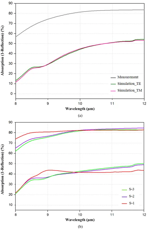
The absorption measurements of the fabricated pixel arrays are done by using a Bruker Vertex 70 FTIR Spectrometer, (with Hyperion 2000 Microscope attachment), with a 35x objective. The reflection data is read by the aid of the system, the absorption values are calculated from the obtained data similar to the case with the simulations. Figure 4 (a) and 4 (b) compare the simulated and measured absorption results of both the reference and the plasmonically enhanced microbolometer individual pixels. Since the pixel is symmetric, there is no significant difference between the TE and
(a) (b)
90 80 70 60 -50 40 30 20 10 o 9 10 11 12 90 80 70 60 50 40 30 20 10 8 9 10 11 12
TM polarizations; Figure 4 (a) also compares the simulation results of the reference pixel in TE and TM polarizations. Consequently, both the simulations and the measurements are performed under unpolarized illumination.
Figure 4. Simulation and measurement comparison graphs of both the reference and the plasmonically decorated pixels respectively. (a) Absorption measurement results for unpolarized illumination of a reference pixel, and the absorption simulation results of the reference pixel in TE and TM polarizations, (b) Absorption measurement and simulation results under unpolarized illumination of the plasmonically decorated pixels. S-1, S-2, and S-3 pixels are described in Figure 2. Since the support arm structures are ignored, and only the pixel bodies are taken into account during the simulations, the simulated absorption values are lower than the experimental values.
A bs orp ti on ( 1-R ef lec tion ) (% ) Wavelength (µm) A bso rp tion (1 -R ef lec tio n) ( % ) Wavelength (µm) Simulation Measurement (b) (a) (b)
Y (fan) .. :. U O U O U .. .. O U Y(Wn) o U O
1
rol
O O Y (Pin) O tEN
O;f
r
OSince the support arm structures of the pixels are not included in the simulations, there is a shift between the simulation and the measurement results. Electromagnetic simulations are done both in TE and TM polarizations. The results plotted are calculated from average of the two polarizations. All of the surface topology occurred during the microfabrication processes are taken into account in the simulations; however the film thicknesses are estimated from the deposition rates. Due to smaller period, there is higher number of features repeated on the S-1 pixel compared to the other two samples’ (Figure 2), and Figure 4 indicates that the absorption enhancement obtained in S-1 pixel is also much stronger. On the other hand, the simulation results are in accord with the FTIR measurement results, the absorption starts to decrease at ~9 µm. The extinction coefficient of the silicon nitride layer around 9 µm clearly starts to increase faster and dominates absorption of the pixel [13], which prevents excitation of surface plasmons in the pixels. The strong material absorption in longer wavelengths overwhelms plasmonic effects.
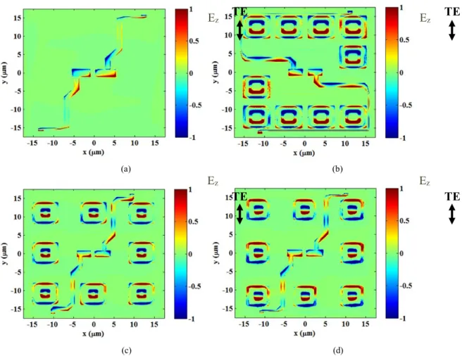
Figure 5 gives the electric field intensity maps (at the z-dimension) of both the reference pixel and the plasmonically enhanced pixels in TE polarizations. The field intensity profiles are shown at the spectral points where the absorption enhancement spectrum exhibits distinctive features. The field profiles exhibit space charge polarization along y-axis and also show capacitive coupling between the inner and the outer squares, which is more evident in the inner squares compared to the outer squares. The maps also indicate that the arms and the electrodes in the middle of the mass also contribute to the coupling. Even the arms and the electrodes in the reference structure show plasmon excitation due to their subwavelength characteristics.
Figure 5. The electric field intensity (color scale) maps (at the z-dimension) of the reference pixel and the pixels decorated with plasmonic features. (a) TE polarization of the reference pixel at 8.5 µm, (b) TE polarization of the S-1 pixel’s body at 8.6 µm, (c) TE polarization of the S-2 pixel’s body at 8.5 µm, (d) TE polarization of the S-3 pixel’s body at 8.5 µm. S-1, S-2, and S-3 pixels are described in Figure 2.
TE TE
TE TE
E
zE
zE
zE
z (a) (b) (c) (d)90
7 8 9 10 11 12 13 14 15
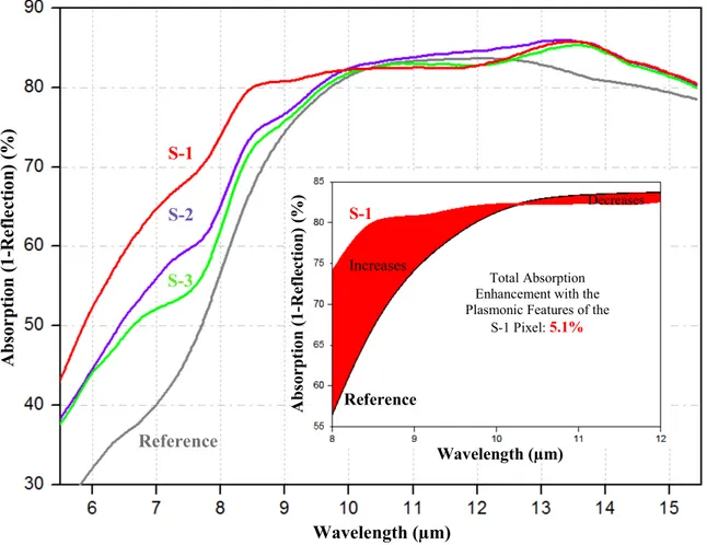
Figure 6 shows the absorption measurement results of both the reference and the plasmonically enhanced microbolometer pixels.
Figure 6. The absorption measurement results of both the plasmonically enhanced pixels and the reference pixel. The maximum absorption is achieved as 5.1% with the S-1, as pointed out in the figure.
While the S-2 and S-3 designs make relatively small contributions to the absorptions, 3.3%, and 1.8% respectively, S-1 results in a very distinct absorption enhancement (5.1%) in a complete microbolometer pixel and increase the absorption from 78% to 82%. The enhancement is much more pronounced between 8 and 9 μm where the silicon nitride is an inefficient absorber [13], the plasmonic features’ surface plasmon excitations make a significant contribution to the pixels’ performance with the other metal layers on the surface. Additionally, the absorption of S-1 between 8-12 µm range has a very good spectral uniformity compared to the reference pixel, which is also another desired property in the uncooled microbolometers.
4. CONCLUSION
We have designed, simulated, and fabricated different microbolometer pixels with different co-centric square ring shaped plasmonic features, and showed the consistency of the simulation and measurement results. We demonstrated 5.1% overall spectral enhancement in the fabricated pixels. A noticeable enhancement with such an easy method in a complete microbolometer pixel is achieved for the first time. There is no need for additional layers or nanolithography techniques, which cost too much. Plasmonic features are placed within the same metal layer of the electrodes and the arms that already exist in a standard microbolometer. The arms and the electrodes also act like the plasmonic structures;
Absor
ption (1
-R
ef
le
ct
io
n)
(%
)
Increases Decreases A b so rpt io n ( 1-R ef le ct ion) ( % )Wavelength (µm)
Wavelength (µm) Total Absorption Enhancement with the Plasmonic Features of theS-1 Pixel:5.1% S-1
S-1
S-2
S-3
Reference
Referencehence they contribute to increase the absorption in the LWIR range. As a result, this study presents a very simple and a very cost effective method to make an absorption enhancement in a complete microbolometer pixel.
REFERENCES
[1] Tanrikulu, M. Y. “An uncooled infrared microbolometer detector array using surface micromachined MEMS technology,” Ph.D. Dissertation, Middle East Technical University, Department of Electrical and Electronic Engineering, (2007).
[2] Beeman, J. W., Nyaiesh A. R., Haller, E. E., Hansen, W. L. and Garwin, E. L., “Diamond-like antireflective coatings for far infrared photoconductors,” European Materials Research Society, Strasbourg, France, (1987). [3] Jayasinghe, J. A. R. C., "Multiband detectors and application of nanostructured anti-reflection coatings for
improved efficiency," Ph.D. Dissertation, Georgia State University, Department of Physics and Astronomy, (2012).
[4] Krenz, P. M., Tiwari, B., Szakmany, G. P., Orlov, A. O., Gonzalez, F. J., Boreman, G. D. and Porod, W., “Response increase of IR antenna-coupled thermocouple using impedance matching,” IEEE Journal of Quantum Electronics 48(5), 659-664 (2012).
[5] Sheng, X., Johnson, S. G., Michel, J. and Kimerling, L. C., “Optimization-based design of surface textures for thin-film Si solar cells,” Optics Express 19(S4), A841-A850 (2011).
[6] Unlu, M. S., Strite, S., “Resonant cavity enhanced photonic devices,” Journal of Applied Physics 78(2), 607-639 (1995).
[7] Spinelli, P., Ferry, V. E., van de Groep, J., van Lare, M., Verschuuren, M. A., Schropp, R. E. I., Atwater, H. A.
and Polman, A., “Plasmonic light trapping in thin-film Si solar cells,” Journal of Optics 14(2), 024002/1- 024002/11 (2012).
[8] Huang, X., El-Sayed, M. A., “Plasmonic photo-thermal therapy (PPTT),” Alexandria Journal of Medicine 47(1), 1-9 (2011).
[9] Brolo, A. G., “Plasmonics for future biosensors,” Nature Photonics 6(11), 709-713 (2012).
[10] Csete, M., Sipos, A., Szalai, A., Najafi, F., Szabo, G. and Berggren, K. K., “Improvement of infrared single-photon detectors absorptance by integrated plasmonic structures,” Scientific Reports, 3(2406), 1-10 (2013). [11] Verhagen, E., “Subwavelength light confinement with surface plasmon polaritons,” Ph.D. Dissertation, Utrecht
University, (2009).
[12] Lulec, S. Z., Kucuk, S. E., Battal, E., Okyay, A. K., Tanrikulu, M. Y. and Akin, T., “An analysis for the broadband absorption enhancement using plasmonic structures on uncooled infrared detector pixels,” Proc. of SPIE 8353, 83531D (2012).
[13] Erturk, O., Battal, E., Kucuk, S. E., Okyay, A. K. and Akin, T., “A plasmonically enhanced pixel structure for uncooled microbolometer detectors,” Proc. of SPIE 8704, 87041E (2013).