Control of the responsivity and the
detectivity of superconductive edge-transition
YBa
2
Cu
3
O
7
ⴚx
bolometers through substrate properties
Mehdi Fardmanesh, Kevin J. Scoles, and Allen Rothwarf
The detectivity D* limits of YBa2Cu3O7⫺xbolometers on 0.05-cm-thick crystalline substrates are
inves-tigated, and a method to increase D* to greater than 109 共cm Hz1兾2兲兾W at a 20-m wavelength is
proposed. Because the response increases proportionally with the bias current Ib, whereas the noise
near Tc共the transition or critical temperature兲 of our MgO and SrTiO3substrate samples does not, an
increase in D* of these samples is obtained by an increase in Ib. Another limiting factor is the dc thermal
conductance G共0兲 of the device, which, although controlled by the substrate-holder thermal boundary resistance for our samples, can be changed by means of thinning the substrate to increase D*. The optimal amount of thinning depends on the substrate’s thermal parameters and the radiation modulation frequency. D* in our samples is also found to follow the spectral-radiation absorption of the substrate material. © 1999 Optical Society of America
OCIS codes: 040.3060, 230.0040.
1. Introduction
There have been many reports of observations of the intrinsic and the nonintrinsic responses of high-Tc 共the critical temperature from the normal to the su-perconducting state兲 superconductive bolometers 关primarily when using YBa2Cu3O7⫺x 共YBCO兲
mate-rials兴 that are higher than the expected values for a purely bolometric response. The interpretation and the analysis of the higher-than-expected values are found to be strongly dependent on the thermal prop-erties of the substrate, the substrate’s dimensions, the superconducting pattern, the modulation-frequency regime with respect to the effective thermal-diffusion length into the substrate, and the electrical and the thermal operating conditions of the detectors. For superconductive edge-transition bo-lometers with flat crystalline substrates that are in direct contact with the cold finger, the effects of
lim-ited dc thermal conductance G共0兲 and Joule heating on the response of the detectors have been misleading factors, resulting in unrealistic values for responsivi-ties and detectiviresponsivi-ties.1,2 This is particularly so for
the low and the midrange modulation-frequency re-sponses of detectors with large-area superconductive meander-line patterns on crystalline substrates such as MgO, LaAlO3, and SrTiO3.3,4
One major source for the above-described misinter-pretation has been the overestimation of the total thermal conductance Gt of the detectors, which is limited by the thermal boundary resistances at the substrate interfaces and not directly by the substrate materials themselves.3–5 These effects are strongly
dependent on the dimensions of the pattern of the superconducting film with respect to those of the sub-strate and on the electrical connections.5
Edge-transition bolometers can be classified as small-area pattern samples 共microbridges兲 and large-area pat-tern samples with respect to the substrate dimen-sions and the substrate thermal parameters. The electrical connections can also be classified as voltage-biased共current response兲 and current-biased 共voltage response兲 four-probe 共or two-probe兲 configu-rations.5
The thermal resistances at the substrate– cold-finger and the superconductor–substrate interfaces need to be used in the design considerations to im-prove the detectivity D*. For an optimal design both M. Fardmanesh共[email protected]兲 is with the
De-partment of Electrical and Electronics Engineering, Bilkent Uni-versity, Ankara 06533, Turkey. K. J. Scoles and A. Rothwarf are with the Department of Electrical and Computer Engineering, Drexel University, Philadelphia, Pennsylvania 19104.
Received 22 April 1999; revised manuscript received 22 April 1999.
0003-6935兾99兾224735-08$15.00兾0 © 1999 Optical Society of America
the electrical and the thermal properties of the de-tectors should be considered. The optimal design parameters are also strongly dependent on the appli-cation and the operating circumstances, mainly the modulation frequency f.
In this paper we present an analysis of the respon-sivity and the detectivity D* of samples with large-area patterns on crystalline MgO, LaAlO3, and
SrTiO3 substrates when measured under a dc bias current in the four-probe configuration. The char-acterized samples are made of 120- to 230-nm-thick
c-axis-oriented YBCO film deposited by use of off-axis
dc planar magnetron sputtering. The samples were patterned by use of standard photolithography that was modified to be less destructive for YBCO mate-rials. Details of the structural and the electrical characteristics of the samples with their deposition parameters and patterning process are given else-where.3,4 The holder or the cold finger in our
exper-imental setup was made of a gold-plated oxygen-free copper disk with an embedded silicon temperature sensor. The sensor was calibrated to a 0.1-K accu-racy, and the OFE copper disk was etched and coated with a layer of gold without being exposed to the atmosphere. A lantern or a Sol-Gel battery with a low-noise metal-film resistor was the current source for measurements of the noise voltage under the four-probe configuration. The measurements were taken with a lock-in amplifier共Princeton Applied Research, Model PAR-5204兲 with an ultralow-noise preampli-fier共Perry, Model 030B; noise limit of 0.4 nV兾Hz1兾2兲
to amplify the voltage signal.
2. Effects of Substrate Properties and Biasing on the Responsivity and the Detectivity Limits
The responsivity of a bolometer is defined as the ratio of the voltage response共in current-biased detectors兲 to the radiation power received by the detector.3,4
The equilibrium responsivity of thin-film supercon-ductive edge-transition bolometers is mainly a func-tion of the substrate properties because the mass of the substrate material is usually much greater than the mass of other components in this type of detector. The thermal and the structural characteristics of the substrate also affect the electrical properties of the superconducting film6; these effects are considered in
Subsection 2.B, below. The electrical biasing is also a major determining factor in the response, and it needs to be considered before further discussion of the effects of substrate properties on the response.
A. Responsivity and Effects of Biasing Configurations
Self-heating, or Joule heating, is a major factor in the bolometric response because the bolometer operates within the resistive transition region of the supercon-ductor near the maximum in dR兾dT. The ac com-ponent is caused by the change in the operating-point resistance that results from the input radiation power and produces positive feedback for current-biased共dc兲 detectors in the four-probe measurement configuration. Taking the positive feedback into ac-count in the equation for the responsivity of
bolom-eters4 allows the overall frequency-dependent
responsivity rfto be obtained from7
rf⫽
Ib
Gt⫹ j2fCt⫺ Ib2共dR兾dT兲 dR
dT, (1) where Ibis the dc bias current, is the fraction of the incident power absorbed by the bolometer 共the ab-sorption coefficient兲, dR兾dT is the slope of the resis-tance R versus the temperature T curve at the bias point, and Gt and Ct are the frequency-dependent total thermal conductance and heat capacity of the bolometer, respectively, which are governed mainly by the substrate properties in most cases.4 As
shown in Eq.共1兲, there is a stability criterion in the voltage response that has the same form as that ob-tained for dc biasing at zero frequency.4
For dc voltage-biased detectors 共constant voltage across the samples兲, the response is in the form of current variations, and Joule heating in the film pro-duces negative feedback.8 This negative feedback
decreases the responsivity, changing the sign of the Joule heating term 关Ib2共dR兾dT兲兴 in Eq. 共1兲. This
negative feedback can improve the dynamic range of voltage-biased detectors by stabilization of the bias temperature at high radiation intensities. This is the situation when the sample is biased such that the Joule heating is comparable with the total absorbed-radiation power. The effects of different electrical connections on the thermal runaway of such detec-tors with different patterns were studied and pre-sented elsewhere.5 The effect of the Joule heating
term in Eq.共1兲 in our samples is negligible for the bias currents used, regardless of the substrate material.3,4 B. Effects of Substrate-Dependent Film Properties on the Detectivity D*
The detectivity D* of the bolometers is a function of the responsivity, the absorbing area共and its absorp-tion coefficient兲, and the intrinsic noise in the device. The detectivity D* of an edge-transition superconduc-tive bolometer versus the temperature is a function of the voltage responsivity and the noise, defined as D* ⫽ 共A⌬f 兲1兾2r
f兾Vn, where A is the radiation-absorbing area in centimeters squared, Vnis the voltage noise, and⌬f is the frequency range used to obtain the noise measurement. The frequency range ⌬f is 1 Hz in this study, giving D* in units of centimeters times square-root hertz per watt. With Eq.共1兲, D* might be improved by an increase in the responsivity by use of higher dc bias currents. This possibility depends on the dependence of the ultimate responsivity and the noise voltage on the bias current, which is dis-cussed in Subsection 2.C.
When ac Joule heating is negligible, as is the case for the currents in our samples, the responsivity in-creases linearly with Ib, as given in Eq.共1兲. Hence
D* can be improved by an increase in Ibif the signal-to-noise ratio also increases. This increase in the signal-to-noise ratio requires that the noise increase with Ib at a rate less than that of the responsivity. Noise in our YBCO samples was found to be
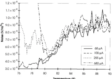
depen-dent on the bias current and the modulation fre-quency and also was found to be strongly temperature dependent. Four major types of volt-age noise are identified in our dc current-biased sam-ples according to where they occur in the temperature range relative to Tc-onset and Tc-zero.3–9 The Tc-onset in our samples is considered to be the point above which the resistance starts to show linear behavior versus the temperature, and Tc-zerois considered to be the point below which the resistance drops to less than 1% of its value at Tc-onset. Although both Tc values are dependent on the bias current, the values of Tc-zeroof our samples are found to be strongly de-creased versus the bias current, depending on the granularity of the films.5 The measured voltage
noise versus the temperature at different values of Ib in the region of interest for sample 064-02b, which was made of 120 –130-nm-thick patterned granular YBCO film on a crystalline MgO substrate, is shown in Fig. 1, and the resistance versus the temperature of the sample is reported elsewhere.5
The noise from approximately the middle of the transition to Tc-onset in our samples with MgO and SrTiO3 substrates is found to be dependent on the
bias current Iband scaled as
Vn⫽ C1⫹ C2Ib, (2)
where C1 and C2 are constants and differ from one
sample to another, with C1 ⬎ C2Ib just less than
Tc-onset, for almost all the samples measured on MgO and SrTiO3 substrates.9 The noise in our samples
with LaAlO3substrates is found to be much higher in
this region. The observed high level of noise in films on LaAlO3 substrates may be due to the high
gran-ularity共twined grains兲 typical of this type of material. As shown in Fig. 1, the voltage noise of the sample with a MgO substrate near Tc-zeroincreases strongly with increasing bias current. But, in the tempera-ture region near the middle of the transition from T⫽ 81 K to T⫽ Tc-onset, the voltage noise follows Eq.共2兲.
In this region the noise increases by only approxi-mately 20%, whereas the bias current increases by a factor of 10. This type of noise is interpreted to be current-dependent fluctuations in the volume frac-tion of the superconducting phase along the current path.9 The same types of bias-current and
temper-ature dependence of the noise voltage in the same temperature region is observed for our other samples on MgO and SrTiO3substrates.3,9 If we consider the
current dependence of the noise, sample substrates that have sharper transitions共higher dR兾dT兲, which lead to lower Ibvalues for the maximum responsivity, are more favorable in this respect. The highest dR兾dT is also found to be at the lower end of the above-given noise-voltage temperature region.9
Hence, because the responsivity is proportional to the bias current Ib, the detectivity D* of samples on MgO and SrTiO3 substrates will increase by means of
in-creasing the bias current Ibif the sample is biased in this temperature region. This increase is limited by the thermal runaway that results from the dc Joule heating in the device and the limits of the responsiv-ity, which are discussed in Subsection 2.C.
C. Effects of Substrate Properties and the Bias Current on Responsivity Limits
Owing to the limited thermal conductance of the de-tectors, which is determined mainly by the substrate properties, dc Joule heating共self-heating兲 is a major limiting factor to the use of high bias currents to obtain higher responsivity, hence higher D*, values. Self-heating can cause an excessive temperature rise ⌬Tdcin the film with respect to the temperature of the
sample holder in which the temperature sensor is normally placed. The resulting ⌬Tdc can occur
mainly across the substrate material or across the substrate– cold-finger thermal boundary resistance region. The region is determined by the relative di-mensions of the superconductive-film pattern com-pared with the thickness of the substrate. The relative dimensions of the film and the substrate de-termine the dominating factor that limits the dc ther-mal conductance G共0兲.
For patterns with dimensions much smaller than the substrate thickness ds, G共0兲 is limited by the lateral heat flow through the superconductive film and the heat diffusion into the substrate material.10 –14 G共0兲 and the heat diffusion are highest
for the samples with MgO substrates because they have the highest thermal conductivity. In samples with pattern dimensions comparable with or larger than their substrate thickness ds, G共0兲 is limited by the thermal resistance at the substrate boundaries and is not strongly dependent on the substrate ma-terial.3,15 In our samples ⌬T
dc is found to occur
mainly at the substrate– cold-finger interface because the dimensions of the meander-line patterns are com-parable with those of the substrate.3,4
Regardless of the dominating factor that deter-mines the total thermal conductance Gt, the dc bias current at any temperature higher than Tc-zerois
lim-Fig. 1. Noise versus the temperature of sample 064-02b on a 0.025-cm-thick MgO substrate at 10 KHz for 68-, 100-, 255-, and 680-A bias currents with Tc-zero共at 100 A兲 ⫽ 73 K and Tc-onset⫽
ited by thermal runaway, which is characterized by the factor␣, defined as4
␣ ⫽ Ib2
G共0兲
dR
dT, (3)
with␣ ⬍ 1 required for stability. As given in Eq. 共3兲, for substrates that yield films with sharper transi-tions such as SrTiO3 the ultimate allowed bias
cur-rent Ib would be lower. The effect of instability in the temperature of the film caused by high bias cur-rents will appear as an unrealistically sharp transi-tion in the R versus T curve.2,5,16 The increase of the
response that is due to the sharper transition dR兾dT dominates the effect of this decrease in the maximum allowed Ibin Eq.共3兲, producing an overall increase in the responsivity for films with sharper transitions. The maximum bias currents Ib-maxof the character-ized samples obtained for␣ ⫽ 0.4 are given in Table 1. If we consider the maximum Ibdetermined by Eq. 共3兲 the magnitude of the maximum responsivity fol-lows 兩rf兩max⫽ Gt
冋
␣G共0兲 1⫹ 共2f兲2 dR dT册
1兾2 , (4)where ⫽ Ct兾Gt.4 Hence from Eq. 共4兲 we can see
that devices on substrates with lower thermal con-ductivities and lower heat capacities and that allow a higher dR兾dT in the transition region will yield the highest responsivities. This result favors devices with SrTiO3substrates when compared with devices
with MgO and LaAlO3 substrates for the same superconducting-film and substrate dimensions. This relation is confirmed by the measurements in the modulation-frequency range of the responsivity governed by Eq.共4兲. The rmaxobtained for the char-acterized samples and their superconducting-pattern dimensions are given in Table 1.
As given in Eq.共4兲, 兩rf兩maxcan be increased by an
increase in G共0兲 when scaled as G共0兲1兾2. This
in-crease in兩rf兩max occurs when the value of Gtat the operating frequency is different from that of G共0兲 at midrange or higher frequencies.4 At very low
fre-quencies, i.e., lower than a critical value f1, Gtmay become equal to or comparable with G共0兲.4 The
value of f1depends on the substrate properties and is the frequency at which the thermal-diffusion length
into the substrate approaches the substrate thick-ness. Then兩rf兩maxdecreases by an increase in G共0兲
when scaled as G共0兲⫺1兾2. The change of the deter-mining factor for Gt affects the slope of the curve of the response magnitude versus the modulation fre-quency. For f⬍ f1the response scales as f⫺1, and for f⬎ f1it scales as f⫺1兾2共Refs. 4 and 17兲. This scaling
is a function of substrate properties and is discussed in Subsection 2.D.
D. Substrate-Material Dependence of the
Substrate-Thickness Effects on the Responsivity Limits
We consider the thermal resistance at the film– substrate interface to be negligible compared with that of the substrate material and the substrate– cold-finger interface in the low and the midrange frequencies.3,4 Then the overall thermal
conduc-tance Gt is determined by the thermal-diffusion length Lfof the absorbed energy共by the superconduc-tive film兲 into the substrate. The quantity Lf, the thermal-diffusion length, represents the characteris-tic penetration depth of the temperature variation into the substrate and is given by
Lf⫽
冉
D
f
冊
1兾2
, (5)
where D⫽ ks兾csand ks and cs are the thermal con-ductivity and the heat capacity, respectively, of the substrate material.
If we consider Lfto be the effective length for the ac heat flow into the substrate in the modulation-frequency range where Lfis less than the substrate thickness 共i.e., f ⬎ f1兲, Gt will be determined by the substrate material and will increase with the fre-quency, scaling as f1兾2共Ref. 4兲. Hence, for a detector operating above f1, the substrate thickness doesn’t affect the responsivity, and兩rf兩maxis governed by Eq.
共4兲, with the substrate thermal parameters as the determining factors. This trend is valid for frequen-cies at which the thermal conductance of the super-conductive film and the film–substrate interface are negligible.4
When the frequency decreases to less than the val-ues at which Lfbecomes comparable with or larger than the substrate thickness 共i.e., f ⬍ f1兲, Gt ap-proaches G共0兲, and the substrate–cold-finger bound-ary resistance Rs⫺c⫽ 1兾Gs⫺cwill be the determining Table 1. Thermal and Electrical Parameters and Dimensions of the Superconductive Film and the Substrates of Samples with SrTiO3, MgO, and
LaAlO3Substratesa Sample Number Substrate Material Cs 共J兾k cm3兲 Ks 共W兾k cm兲 ds 共cm兲 G共0兲 共mW兾K兲 dR兾dT 共⍀兾K兲 df 共nm兲 A 共cm2兲 Ib-max 共mA兲 rmax 共V兾W兲 D* 共cm Hz1兾2兲兾W 064-01 SrTiO3 0.43 0.052 0.05 3 1800 220 0.017 0.66 400 3.6⫻ 10 7 064-02b MgO 0.53 3 0.025 15.5 950 120 0.075 2.08 127 0.3⫻ 106 064-03a MgO 0.53 3 0.05 11 1000 170 0.075 1.66 151 064-04 LaAlO3 0.59 0.16 0.05 7.8 2200 190 0.075 1.0 274 1.8⫻ 10 6 aThe value of D* given was obtained for a 100-Hz modulation frequency and a 20-m wavelength. The term d
fis the thickness of the
YBCO film, dsis the thickness of the substrate, G共0兲 is the measured dc substrate–cold-finger thermal boundary resistance, A is the total
area of the superconducting pattern, rmaxis the maximum zero modulation-frequency response, and Ib-maxis the maximum allowed bias
factor in the total thermal conductance. In our sam-ples Rs⫺cvalues are found to be much larger than the
thermal resistance of the substrates, giving G共0兲 ⬵
Gs⫺c. For共2f兲2 ⬎⬎ 1 and while still valid in the
above frequency range4with G
t⬵ G共0兲 in Eq. 共4兲, the maximum responsivity is 兩rf兩max⫽ 2fCt
冋
␣G共0兲dR dT册
1兾2 . (6)Hence under the above conditions and within this frequency regime共 f ⬍ f1兲 thinning the substrate will
increase rfby means of decreasing Ctas long as the bias current does not exceed the critical current value
Icof the superconducting film. The thermal bound-ary resistance at the substrate– cold-finger interface 1兾G共0兲 is also found to decrease from thinning of the substrate, regardless of the substrate materials. Possible mechanisms for this result were presented elsewhere.3 For large-area patterns the decrease in G共0兲 is found to be approximately proportional to the
substrate thickness ds. Hence, by considering Ct also to be proportional to the substrate material’s thickness, we find that thinning the substrate is ex-pected to increase 兩rf兩max by approximately 共dsi兾
dsf兲
3兾2, where d
siand dsfare the initial and the final
substrate thicknesses, respectively.
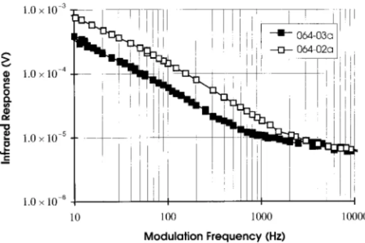
The effects of the modulation frequency on the re-sponse in different frequency regimes for two samples with identical meander-line patterns on 0.025- and 0.05-cm-thick crystalline MgO substrates are shown in Fig. 2. At high frequencies at which Lf is less than the substrate thickness for both samples, the responsivities are equal, and the response is deter-mined by the characteristics of the superconducting pattern and the substrate material. For lower fre-quencies at which Lfis greater than the thickness of the substrates the response of the sample with the thinner substrate共sample 064-02a兲 is higher. This result is mainly due to differences in the values of Ct, which is approximately proportional to the thickness of the substrates because the bias currents are same
共1 mA兲. The maximum responsivity of the 0.025-cm-thick substrate sample 共064-02a兲 is approximately 2.8 times higher than that of the 0.05-cm-thick sub-strate sample 共064-03a兲, also because of the differ-ences in the G共0兲 values as well as the in Ctvalues.
If a detector is used in a bridge 共microbolometer兲 configuration,18 G
t will be determined primarily by the lateral heat flow through the substrate. Be-cause dsis still much larger than the film thickness, the resulting heat flow through the film is negligible. In this configuration thinning the substrate will also increase rf, mainly by means of lowering Ct.10,18 Thinning the substrate in this case will cause a de-crease in the value of G共0兲 of the detector by reduction of the area of the lateral thermal-conduction path through the substrate material. This reduction yields an increase in 兩rf兩max that is lower than the
expected value and scales as共dsi兾dsf兲
1兾2. The
mini-mum required thickness of the substrate Lm versus the modulation frequency beyond which the respon-sivity increases by means of further thinning is cal-culated for the three substrate materials, and the results are shown in Fig. 3.
3. Spectral Responsivity and Substrate-Material Properties
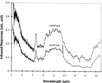
The spectral responsivity of sample 064-01a when measured to as high as 20m at two bias currents is shown in Fig. 4. The sample is made of a 220 –230-nm YBCO superconductive film on a 0.05-cm-thick crystalline SrTiO3 substrate. The super-conductive pattern is a 50-m-wide and 1.9-cm-long meander line with a total area of 0.0168 cm2共Ref. 9兲.
The magnitude of the response shown in Fig. 4 is proportional to Ib, whereas the spectral response fol-lows the spectral absorption of the substrate mate-rial, as shown in Fig. 5. This relation is interpreted to be due to the absorption of radiation in the open areas of the substrate between the meander lines with the flow of heat to the superconductor. The spectral absorption of the substrates is derived di-rectly by use of the spectral reflectance and transmit-tance of a 0.05-cm-thick bare substrate. The measured spectral absorption of the SrTiO3substrate Fig. 2. Measured response versus the modulation frequency for
samples with a 0.05-cm-thick MgO substrate共sample 064-03a兲 and a 0.025-cm-thick MgO substrate共sample 064-02a兲 by use of a 1-mA bias current and a 2.13-mW兾cm2radiation intensity.
Fig. 3. Calculated Lmversus the modulation frequency for
is slightly different from that obtained by use of clas-sical dispersion theory19 –21and shows a particularly
strong peak at an approximately 7.5-m radiation wavelength, as observed in both Figs. 4 and 5.
As shown in Fig. 4, the response of the SrTiO3
substrate sample also follows the trend for the ab-sorption in thin-film and single-crystal YBCO mate-rials, increasing at shorter wavelengths.22,23 Using
the ratio of the change in the response resulting from substrate absorption with respect to that of the film shows that the fraction of the power absorbed by the substrate can be obtained at any wavelength. As derived for sample 064-01a 共the SrTiO3 substrate兲,
approximately 50% of the response at 10 m and more than approximately 75% of the response at 20 m are due to the absorption of the incident radiation in the open areas of the substrate. The effects of substrate absorption on the response dominate at some longer wavelengths共i.e., 20 m兲 at which ab-sorption by the superconducting film is reduced even further.22,23 The absolute value of the responsivity
for the above-described sample was measured at 7.39
m with a 500-K blackbody source. A response of 1.582 V is obtained for a radiation intensity of 5.64 ⫻ 10⫺4 W兾cm2 at a 400-Hz modulation
fre-quency and a 300-A dc bias current. A responsiv-ity of 0.5 V兾W and a detectivity D* of 0.72 ⫻ 106共cm
Hz1兾2兲兾W are obtained under the above conditions.
4. Engineering Changes for a Higher Detectivity D*
As an example of the engineering changes required to increase D* by use of the analysis presented in this study, we present an analysis of the sample on the SrTiO3 substrate. From the spectral response
shown in Fig. 4 and by use of a maximum bias current of 0.66 mA from Table 1 a D* of approximately 3.6⫻ 107共cm Hz1兾2兲兾W is obtained for the sample with the
SrTiO3 substrate 共064-01a兲 at a 20-m wavelength
and a 100-Hz modulation frequency. The spectral detectivity at a constant bias current and a constant temperature follows the spectral response of the de-tector for a constant radiation intensity. The D* of the characterized samples at the 20-m wavelength is given in Table 1.
For increasing D* consider the 400-Hz and the 100-Hz modulation-frequency points in Fig. 3 as ex-amples. The substrate of sample 064-01a should be thinned to less than 0.01 and 0.02 cm, respectively. The substrate can be thinned by use of a wet-etching method after the patterning process for the supercon-ductive film. Thinning the substrate will also in-crease G共0兲 while it is still limited by Rs⫺c. On the
basis of the above analysis, thinning the substrate to 0.005 cm with an increase in the total area of the superconductive pattern of as much as 0.09 cm2
yields a D* of the order of 1⫻ 109共cm Hz1兾2兲兾W at 20 m for 200-nm-thick YBCO superconducting films on crystalline SrTiO3 substrates. Also, as observed
from Eq.共2兲 and Table 1, the detectivity of the sam-ples can be enhanced by a sharper transition共favored by the substrates’ lattice structures兲 because it allows lower Ib-max values, hence lower current-dependent noise in the region. Again, this leads to the SrTiO3 substrate as the most favorable of the substrate ma-terials investigated in this study.
5. Summary and Conclusions
The ultimate detectivity of an edge-transition super-conductive bolometer is determined by the maximum responsivity兩rf兩maxand the current dependence of the
noise at the operating temperature. The D* of our samples with MgO and SrTiO3 substrates has been
found to increase with an increase in the bias current
Ib because the noise voltage in the temperature re-gion of interest共in the middle of the transition region兲 near Tcdoes not increase significantly with Ibin this region. For samples with LaAlO3 substrates this trend has not been observed because there is exces-sive noise in the whole transition region. This result leads to the samples with SrTiO3 substrates as the
most favorable of the substrates investigated in this study because the films on SrTiO3substrates have a
sharper transition dR兾dT compared with those on MgO substrates. The maximum responsivity is set
Fig. 4. Spectral response of a sample with a 0.05-cm-thick SrTiO3
substrate共sample 064-01a兲 at 0.55- and 0.97-mA bias currents.
Fig. 5. Measured spectral absorption of samples with 0.05-cm-thick crystalline SrTiO3, MgO, and LaAlO3substrates.
by the limits on the dc bias current that are deter-mined from the dc Joule heating and the dc thermal conductance of the device G共0兲, which is set by the substrate– cold-finger thermal boundary resistance in our samples.
Thinning the substrates of the samples to increase the maximum responsivity 兩rf兩max depends on the
variations of the total thermal conductance Gt and the total heat capacitance Ctof the device. The crit-ical required thinning of the substrates Lm below which the responsivity increases has been found to be dependent on the substrate materials and the mod-ulation frequency f, scaling as f⫺1兾2. In a frequency regime that is low enough that the thermal-diffusion length into the substrate is greater than the sub-strate thickness, Lf ⬎ ds, thinning the substrate of the detector increases兩rf兩maxby a factor of共dsi兾dsf兲3兾2,
where dsi and dsf are the initial and the final
sub-strate thicknesses, respectively. In the higher-frequency regime in which Lf ⬍ ds, thinning the substrate of the detector increases兩rf兩maxby
approx-imately共dsi兾dsf兲 1兾2.
Substrate absorption has been shown to be the determining factor in the spectral responsivity, hence in the detectivity, for the infrared to the far-infrared wavelengths at which the absorption of the superconducting films is strongly reduced com-pared with their values at shorter-radiation wave-lengths. This property of the substrates can be used for selective wavelength sensitivity for an edge-transition superconducting infrared detector. The spectral absorption of our SrTiO3 substrates has been found to deviate from the theoretical val-ues obtained by use of classical dispersion theory, particularly at 7.5m. A detector of 0.09 cm2, an overall patterned superconducting area, and a D* of the order of 1 ⫻ 109 共cm Hz1兾2兲兾W at 20 m on a crystalline SrTiO3 substrate can be obtained if the
substrate is thinned to 0.005 cm.
In conclusion, the effective heat conductivity, the effective heat capacity, and the substrate-dependent film quality in terms of low noise and sharp transitions have been shown to be the major factors in choosing a substrate material in this type of bolometer. For a YBCO edge-transition bolom-eter operating at wavelengths from the near infra-red to the far infrainfra-red the spectral absorption of the substrate material will also be another factor to be considered if the open areas of the substrate are comparable with or larger than the absorbing sur-face area of the superconducting film. For a uni-form spectral response coating the superconducting pattern area with a material that has an absor-bance that is independent of wavelength is advis-able. However, for making the bolometer sensitive to a narrow band of wavelengths coating it with a material that absorbs strongly at those wave-lengths is recommended if the selective absorbance of the substrate is not within the desired range of wavelengths.
The author would like to thank Sefik Suzer for his help with the spectral-absorption measurements of the substrates.
References
1. J. H. Hao, F. Q. Zhou, H. D. Sun, X. J. Yi, and Z. G. Li, “Responsivity calculation and measurement of YBaCuO opti-cal detector,” IEEE Trans. Appl. Supercond. 3, 2167–2169 共1993兲.
2. H. Chou, H. Z. Chen, M. T. Hong, Y. C. Chen, and T. C. Chow, “Bolometric detection in a precipitation free YBa2Cu3O7⫺xfilm
at 77 K,” Appl. Phys. Lett. 68, 2741–2743共1996兲.
3. M. Fardmanesh, A. Rothwarf, and K. J. Scoles, “YBa2Cu3O7⫺x
infrared bolometers: temperature dependent responsivity and deviations from the dR兾dT curve,” J. Appl. Phys. 77, 4568 – 4575共1995兲.
4. M. Fardmanesh, A. Rothwarf, and K. J. Scoles, “Low and midrange modulation frequency response for YBCO infrared detectors: interface effects on the amplitude and phase,” IEEE Trans. Appl. Supercond. 5, 7–13共1995兲.
5. M. Fardmanesh, K. J. Scoles, and A. Rothwarf, “DC charater-istics of patterned YBa2Cu3O7⫺x superconducting thin film
bolometers: artifacts related to Joule heating, ambient pres-sure, and microstructure,” IEEE Trans. Appl. Supercond. 8, 69 –78共1998兲.
6. J. M. Phillips, “Substrate selection for high-temperature su-perconducting thin films,” J. Appl. Phys. 79, 1829 –1848共1996兲. 7. M. Fardmanesh, A. Rothwarf, and K. J. Scoles, “The respon-sivity and detectivity limits for patterned YBa2Cu3O7⫺x
super-conductive IR-detectors,” in Proceedings of the Sixth International Superconductive Electronics Conference, H. Kock and S. Knappe, eds.共Physikaisch-Technidsche Bundesanstalt, Berlin, 1997兲, Vol. 3, pp. 399–401.
8. K. D. Irwin, G. C. Hilton, D. A. Wollman, and J. M. Martinis, “X-ray detection using a superconducting transition-edge sen-sor microcalorimeter with electrothermal feedback,” Appl. Phys. Lett. 69, 1945–1947共1996兲.
9. M. Fardmanesh, A. Rothwarf, and K. J. Scoles, “Noise charac-teristics and detectivity of YBa2Cu3O7superconducting
bolom-eters: bias current, frequency, and temperature dependence,” J. Appl. Phys. 79, 2006 –2011共1996兲.
10. G. D. Poulin, J. Lachapelle, S. H. Moffat, F. A. Hegmann, and J. S. Preston, “Current–voltage characteristics of dc voltage biased high temperature superconducting microbridges,” Appl. Phys. Lett. 66, 2576 –2578共1995兲.
11. A. V. Sergeev, A. D. Semenov, P. Kouminov, V. Trifonov, I. G. Goghize, B. S. Karasik, G. N. Gol’tsman, and E. M. Gershen-zon, “Transparency of a YBa2Cu3O7-film–substrate interface
for thermal phonons measured by means of voltage response to radiation,” Phys. Rev. B 49, 9091–9096共1994兲.
12. S. J. Bae, S. Hong, E. Kim, W. Shin, C. H. Cho, Y. K. Kim, Y. S. Bea, T.-H. Sung, and K. No, “Effect of texturing and micro-bridge length on the responsivity of YBa2Cu3Oxthin film,” Jpn.
J. Appl. Phys. 35, 1716 –1719共1996兲.
13. M. Nahum, Q. Hu, P. L. Richards, S. A. Sachtjen, N. Newman, and B. F. Cole, “Fabrication and measurement of high Tc
su-perconducting bolometers,” IEEE Trans. Magn. 27, 3081–3084 共1991兲.
14. U. P. Oppenheim, M. Katz, G. Koren, E. Polturak, and M. R. Fishman, “High temperature superconducting bolometer,” Physica C 178, 26 –28共1991兲.
15. P. E. Phelan, “Thermal response of thin-film high-Tc
super-conductors,” J. Therm. Phys. Heat Transfer 9, 397– 402共1995兲. 16. D. Janik, D. May, H. Wolf, and R. Schneider, “High-Tc
transition-edge bolometer for detecting guided millimeter waves,” IEEE Trans. Appl. Supercond. 3, 2148 –2151共1993兲. 17. Q. Hu and P. L. Richards, “Design analysis of a high-Tc
su-perconducting bolometer,” Appl. Phys. Lett. 55, 2444 –2446 共1989兲.
18. T. G. Stratton, B. E. Cole, P. W. Kruse, R. A. Wood, K. Beauchamp, T. F. Wang, B. Johnson, and A. M. Goldman, “High-temperature superconducting bolometer,” Appl. Phys. Lett. 57, 99 –100共1990兲.
19. K. Kamaras, K. L. Barth, F. Keilmann, R. Henn, M. Reedyk, C. Thomsen, M. Cardona, J. Kircher, P. L. Richards, and J. L. Stehle, “The low-temperature infrared optical functions of SrTiO determined by reflectance spectroscopy and spectro-scopic ellipsometry,” J. Appl. Phys. 78, 1235–1240共1995兲.
20. A. S. Barker, Jr., and M. Tinkham, “Far-infrared ferroelectric vibration mode in SrTiO,” Phys. Rev. 125, 1527–1530共1962兲. 21. J. C. Galzerani and R. S. Katiyar, “The infrared reflectivity in SrTiO and the antidistortive transition,” Solid State Commun. 41, 515–519共1989兲.
22. Z. M. Zhang, B. I. Choi, T. A. Le, M. I. Flik, M. P. Siegal, and J. M. Phillips, “Infrared refractive index of thin YBa2Cu3O7
superconducting films,” J. Heat Transfer 114, 644 – 652共1992兲. 23. D. Van der Marel, H. U. Habermeier, D. Heitmann, W. Konig, and A. Wittlin, “Infrared study of the superconducting phase transition in YBa2Cu3O7⫺x,” Physica C 176, 1–18共1991兲.