CRYSTAL GROWTH AND
INVESTIGATIONS ON THE EFFECTS OF
HYDROGEN DOPING OF VO
2a thesis submitted to
the graduate school of engineering and science
of bilkent university
in partial fulfillment of the requirements for
the degree of
master of science
in
materials science and nanotechnology
By
Koray Yavuz
Crystal Growth and investigations on the effects of Hydrogen Doping of VO2
By Koray Yavuz March 2019
We certify that we have read this thesis and that in our opinion it is fully adequate, in scope and in quality, as a thesis for the degree of Master of Science.
Talip Serkan Kasırga(Advisor)
Aykut Erba¸s
Abdullah Ceylan
Approved for the Graduate School of Engineering and Science:
Ezhan Kara¸san
ABSTRACT
CRYSTAL GROWTH AND INVESTIGATIONS ON THE
EFFECTS OF HYDROGEN DOPING OF VO
2Koray Yavuz
M.S. in Materials Science and Nanotechnology Advisor: Talip Serkan Kasırga
March 2019
Vanadium Dioxide(VO2) has been studied extensively for its interesting electronic structure that allows it to go through Metal-Insulator Transition(MIT) at 65◦C. The nature of this phenomena is not entirely clear and more research is needed to firmly establish the science behind it and to realize possible applications; such as ultra-fast electrical and optical switching, sensor devices and Mott-Field Effect Transistors. One of the important experiments to understand the electronic structure of a material is Hall-effect measurements but due to acicular (needle like) nature of VO2crystals, this subject is only studied either on millimeter sized
samples which are not suitable for many device applications or on poly crystalline thin films that are under non-uniform stress due to the substrate effects which gives unsatisfactory results when performing experiments. This thesis suggest a new method of chemical vapour deposition(CVD) growth for low aspect ratio VO2 crystals that have lengths between 50-100 µm and thicknesses between
40-170 nm. These crystals can be mechanically removed from the substrate and transferred to use in different applications such as Hall-effect measurements or Transmission Electron Microscope(TEM) studies. Additionaly this work shows some aspects of the surface chemistry of the widely used Silica, Si, quartz and Sapphire substrates; relating with the control of oxygen saturation on the surface. Another VO2growth method for c-plane sapphire that leads to considerably more
crystal yield is shown.
Hydrogenation of the VO2 crystals suppresses the MIT so understanding
this phenomena might help us better understand the effects lying behind the transition. To study this phenomena a crystal is doped only from half by blocking the passage of hydrogen to other half so the interplay between the insulating phase and hydrogenated conductive phase can be observed. As the analysis tool, TEM is used on this sample. Using a two-terminal device of a VO2 crystal, the effects
iv
of hydrogenation on the electronic properties have also been studied.
Overall this thesis introduces a new method for CVD growth of VO2 which is
used in various applications such as Hall-effect experiments, two terminal devices and TEM studies. To control the growth process the interplay between oxygen and surface chemistry of sapphire, silica, Si and quartz substrates have been investigated. With these studies a better understanding of the mechanics of growth is intended.
Keywords: Vanadium dioxide, Crystal Growth, Strongly Correlated Materials, Metal-Insulator Transition, Hall-effect.
¨
OZET
VO
2KRISTAL B ¨
UY ¨
UTMESI VE HIDROJEN ILE
KATKILANMASININ ¨
UZERINE INCELEMELER
Koray Yavuz
Malzeme bilimi ve Nanoteknoloji, Y¨uksek Lisans Tez Danı¸smanı: Talip Serkan Kasırga
March 2019
Vanadyum Dioksit(VO2), 65 ◦C’da metal-yalıtkan faz ge¸ci¸si g¨osteren g¨u¸cl¨u
etkile¸simli bir materyaldir. Bu faz ge¸ci¸si VO2’nin ¨onemli elektronik ¨ozelliklerinden kaynaklanmaktadır ama bu ¨ozelliklerin do˘gası kesin bir bi¸cimde bilinmemektedir. Faz ge¸ci¸sinin arkasındaki fiziksel nedenler daha iyi bilinebilirse; ultra-hızlı elektriksel ve optik anahtarlama, sens¨or ve Mott-alan etkili transist¨or uygulamalarının hayata ge¸cirilmesine katkı sa˘glanmı¸s olur. Elektronik ¨ozellikleri anlamadaki ¨onemli deneylerden biri Hall efekti deneyidir ama VO2’nin
asik¨uler(i˘gnemsi) do˘gası nedeniyle bu deney sadece ya milimetre boyundaki aygıt yapımı i¸cin uygun olmayan ¨orneklerde ya da d¨uzensiz strese sahip polikristal ince filmlerde ¸calı¸sılmı¸stır ama bu ¨orneklerden alınan ¨ol¸c¨umler tatmin edici de˘gildir. Bu tezde 50-100 µm arası ve 50-170 nm kalınlı˘gında d¨u¸s¨uk en-boy oranlı VO2 kristalleri ¨uretmek i¸cin yeni bir Kimyasal Buhar Biriktirme kristal
b¨uy¨utmesi metodu sunmaktadır. Elde edilen kristaller mekanik olarak b¨uy¨utme altta¸sından alınabilmekte ve Hall etkisi ¨ol¸c¨umleri ya da Ge¸cirimli Elektron Mikroskopu ¸calı¸smaları i¸cin transfer edilebilinmektedir. Ek olarak yaygın olarak kullanılan silika, silikon, kuartz ve safir altta¸sları i¸cin olan y¨uzey kimyası ve oksijen sat¨urasyonu ile ilgili bazı hususlar g¨osterilmi¸stir. Safir c-d¨uzlemindeki VO2 b¨uy¨utmesi i¸cin ¨onemli ¨ol¸c¨ude randıman veren bir metot da geli¸stirilmi¸stir.
VO2 kristallerinin hidrojen ile katkılanması metal-yalıtkan faz ge¸ci¸sini bastırır, bu olayın anla¸sılması faz ge¸ci¸sinin arkasında yer alan etkileri anlamamıza yardımcı olabilir. Yalıtkan faz ile hidrojen ile katkılanmı¸s iletken faz arasındaki ili¸skiyi incelemek i¸cin bir tekil kristal VO2 kiri¸si yalnızca yarısından hidrojenle
katkılanmı¸stır. Analiz i¸cin Ge¸cirmeli Elektron Mikroskobu kullanılmı¸stır. ˙Iki u¸clu bir VO2 aygıtı kullanılarakda hidrojen katkılanmasının kristalin elektronik
¨
vi
¨
Ozetle bu tez Hall-etkisi incelemeleri, iki-u¸clu aygıt yapımı ya da Ge¸cirmeli Elektron Mikroskopu ¸calı¸smalarında kullanılması amacıyla 50-100 µm boyutlarında ve 75-170 nm kalınlı˘gında d¨u¸s¨uk en-boy oranlı tekil kristal VO2’nin Kimyasal Buhar Biriktirme’sinde yeni bir kristal b¨uy¨utme y¨ontemini sunmaktadır. B¨uy¨utme s¨urecini y¨onetmek i¸cin silika, silikon, kuartz ve safir altta¸slarındaki y¨uzey kimyası ve oksijen arasındaki ili¸ski ara¸stırılmı¸stır. Bu metotlarla birlikte VO2’nin kristal b¨uy¨utme mekanizmasının daha iyi anla¸sılması
hedeflenmektedir.
Anahtar s¨ozc¨ukler : Vanadyum dioksit, Kristal B¨uy¨utmesi, G¨u¸cl¨u Etkile¸simli Malzemeler, Metal-Yalıtkan Faz Ge¸ci¸si, Hall-efekti.
Acknowledgement
I would like to thank my advisor Dr. T. Serkan Kasırga for his guidance during my study. I would like to thank to all scmlab members, old and new, whom I’ve learned and received help whenever needed; especially Engincan S¨urmeli and Mustafa Fadlelmula. I would like to thank my parents Kenan Yavuz and Yurdag¨ul Yavuz for their unconditional love and support which is one of the biggest reasons I am able to pursue my career goals. I would also like to thank my brother Kaan Yavuz for his endless support and care. I would like to thank to thank my friends from my old and new dorm, H¨usna, Dilara, Hatice, Nurcan, ˙Ihsan, Denizcan, Gamze, Fulya, Nermin abla, Mustafa Kahraman and many others with whom I’ve had very enjoyable time together and of course dining. Finally, I would especially like to thank U˘gur Te˘gin, Onur C¸ akıro˘glu, Abd¨ullatif ¨Onen, Beg¨un Erbaba, Assel Amirzhanova, Eliza Sopubekova, Ulviyya Quliyeva and ¨Ozge Be˘gli, for their great friendship in which I’ve found immense amount of joy.
Contents
1 Introduction 1
1.0.1 Vanadium Dioxide . . . 2
1.0.2 Structure of Vanadium Dioxide . . . 3
1.0.3 Nature of Metal-Insulator Transition . . . 5
1.0.4 Hydrogen Doping of Vanadium Dioxide . . . 7
1.0.5 Problems that emerge in VO2 Research . . . 8
1.0.6 Outline . . . 9
2 Crystal Growth of VO2 11 2.0.1 Mechanics of crystal growth of VO2 . . . 13
2.0.2 Methods . . . 15
2.0.3 SiO2 substrate . . . 18
2.0.4 VO2 growth Methods . . . 28
CONTENTS ix
2.0.6 Quartz substrate . . . 34
2.0.7 Sapphire c-plane . . . 34
3 TEM Studies of Hydrogen Doped Crystals 39
3.0.1 Methods . . . 42
3.0.2 Results . . . 47
4 Electronic structure changes in VO2 crystal with hydrogen
doping 51
4.0.1 Methods . . . 52
4.0.2 Current State of the Experiments . . . 52
List of Figures
1.1 Schematic band structure of the 3d bands around the Fermi level of VO2. The energy of 0.2 eV is obtained by ultraviolet photoemission
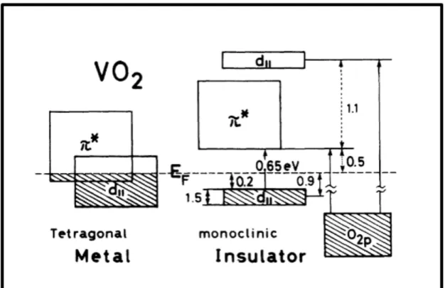
spectroscopy, the energies of 0.5 and 1.1 eV are obtained by ultraviolet reflectance spectra and 0.65 eV is obtained from infrared absorption spectra[1]. Reprinted figure with permission from [Shin, Shik, et al. ”Vacuum-ultraviolet reflectance and photoemission study of the metal-insulator phase transitions in VO 2, V 6 O 13, and V 2 O 3.” Physical Review B 41.8 (1990): 4993.] Copyright (2019) by the American Physical Society. . . 3
1.2 Monoclinic (M1) and Rutile (R) Structures of VO2 . . . 4
2.1 VO2 crystal forming from a fuel dome. Reprinted with permission
from (E. Strelcov, A. V. Davydov, U. Lanke, C. Watts, and A. Kolmakov, “In situ monitoring of the growth, intermediate phase transformations and templating of single crystal vo2 nanowires and nanoplatelets,” ACS Nano, vol. 5, no. 4, pp. 3373–3384, 2011). Copyright (2011) American Chemical Society[2]. . . 14
2.2 (a) shows the crystal equilibrium shape in free space and (b) on a substrate with chemical potency β . . . 15
LIST OF FIGURES xi
2.4 Alumina boat used in the growth a) Both sides of the boat is dented to acommodate a 1cm x 1 cm substrate. b) boat-substrate arrangement, substrate stays upside down so that the growth surface directly faces the precursor with roughly 1 cm distance. The alumina boat and the quartz tube acquires a black color after repeated VO2 growths, but this has no effect on the growth itself
and all of our results are repeatable with clean boat and tube. . . 17
2.5 Optical microscope images of 750-P3 route stopped at certain times after the start of crystal growth period. Three different samples are prepared which show different moments of growth; a) 10 minutes, b) 30 minutes, c) 50 minutes after the start of crystal growth period. 19
2.6 XPS analysis of four different samples prepared with 750-P3 route which were stopped at a) 10 minutes, b) 30 minutes, c) 50 minutes d) 90 minutes after the crystal growth period. The O1s peaks are The +4 phase peak from VO2 doesn’t occur after 10 minutes
and 30 minutes. Vanadium +5 phase peak coming from The V2O5
persist even after 90 minutes due to thin layer of oxidation on the surface of the crystals. The references used for the analysis are: [3][4][5]. . . 20
2.7 Electron microscope pictures of the growths that has been stopped after 15 minutes into the ceasation of oxygen flow at 780◦C. (a), (b), (c) are pictures of P2-780 method. The nucleation rate is pretty high and the domes connect as they come together. The connection lines can be seen at (c). (d), (e), (f) are the images of P3-780 method. The nucleations are much more scarce compared to P2-780. (g), (h), (i) are images of P5-780 method. The nucleation rate is not that much lower than P3-780 but domes that are connected are more scarce. . . 22
LIST OF FIGURES xii
2.8 With no oxygen flow during the heat up period the SiO2 surface
starts to lose its oxygen and takes oxygen from V2O5 domes, starting the nucleation. (a) shows the schematics of this process with (b) showing the optical image of the result, substrate surface fully covered by VO2. When there is 0.2 sccm O2 flow during the
heat up period, surface of the SiO2 substrate doesn’t lose a lot of
oxygen and in turn V2O5 domes have much lower nucleation rate.
(c) shows the schematics of this process and (d) shows the optical image of the result, the domes mostly stay intact without turning to VO2. The temperature during the growth period was 720oC for
both cases . . . 23
2.9 Optical images of growth at 750 ◦C with a) P0, b) P2, c) P3, d) P4 e) P5 routes. . . 24
2.10 Optical images of growth at 780◦C with a) P2, b) P3, c) P4 d) P5 routes. . . 25
2.11 Optical images of growth at 830 ◦C with a) P3, b) P4, c) P5 routes. 26 2.12 Optical images of a) 750-P3 b) 750-P5 routes, the growths were
stopped 10 minutes after the start of the crystal growth period. . 26
2.13 Schematics of proposed dynamics of different morphologies seen in VO2 growth for temperatures between 750-830 ◦C. (a),(b) shows the x≤3 of Px route where VO2 platelets cover the surface. (c)
shows x > 3 where no platelets are seen and the surface is covered with VO2 rods. . . 28
2.14 Optical image of Method-1 growth on SiO2 substrate. During the time that the system was reaching to 790◦C, 0.5 sccm O2flow given
to system. The flow was ceased at 790 ◦C so while the furnace is heated to 950 ◦C with a heating rate of 5 ◦Cmin−1. . . 29
LIST OF FIGURES xiii
2.15 Optical microscope image of crystals grown on 1 µm SiO2substrate
using Method-2 with 780-P5 route. The Scale-Bar is 100 µm. . . . 30
2.16 Schematics for (a) Method-1 where the radiation coming from the heaters is utilized and (b) Method-2 where particles coming from the nitrile glove are utilized to increase the rate of nucleation and the size of crystals. . . 31
2.17 Optical microscope images of various crystals grown using Method-2 with 780-P5 route transferred onto hBN flakes for the use in hall-effect measurement devices. Scale bar is 20 µm. . . 31
2.18 Micro manipulator with tungsten needle tip. All of the VO2 crystals are removed from the surface and transferred using this system. To ease the removing of the crystals from the surface of SiO2 substrate, the substrates are dipped into 1:7 BOE solution
for 2 minutes. If necessary this step is repeated. . . 32
2.19 Optical microscope image of growth of silicon wafer at 780◦C with a) P5, b) P500 routes. . . 33
2.20 Electron Microscope image of growth on silicon wafer at 780 ◦C with a) P5, b) P500 routes. P5 route shows low aspect ratio thin platelets while P500 shows three dimensional shapes due to low chemical potency of the surface. . . 33
2.21 Growth on Quartz substrate at 780 ◦C with a) P0, b) P2 routes. . 34 2.22 Optical microscope image of VO2on c-cut sapphire. (a) No oxygen
flow given to system at heat up period and the temperature was 750
◦C at growth period, (b) 1:3 O
2:Ar flow provided to the chamber
during the heat up period and c) 1:3 O2:Ar flow provided to the
chamber during the heat up period till 750◦C then temperature is raised to 850◦C with rate of 10 ◦C/min. . . 35
LIST OF FIGURES xiv
2.23 Different modes of growth under optical microscope, with VO2
beams and vertical rods. Vertical rods cast shadows on the substrate. . . 36
2.24 Different morphologies of VO2under electron microscope that were
grown on sapphire c-plane substrate. All the scalebars are 20µm. 37
2.25 XRD results for VO2 growth on c-cut sapphire. During the heat up period a growth 1:3 O2:Ar flow provided to the chamber till 750
◦C then temperature is raised to 850 ◦C with 10 ◦C /min. a.u.:
arbitrary units. . . 38
3.1 The monoclinic (M1), tetragonal-rutile (R) and orthorhombic (O1) structures of VO2 are shown, looking from the c-axis for R, O1 structures and slightly misaligned a+c direction for M1. Oxygen atoms are colored red and Vanadium atoms are colored grey. Below the transition temperature, VO2crystal has monoclinic(M1)
structure and above it has rutile(R) structure. With hydrogen doping the lattice structure turns into orthorombic structure with ‘b’ lattice constant of rutile structure getting larger. Reprinted (adapted) with permission from (Filinchuk, Yaroslav, et al. ”In situ diffraction study of catalytic hydrogenation of VO2: Stable phases and origins of metallicity.” Journal of the American Chemical Society 136.22 (2014): 8100-8109). Copyright (2014) American Chemical Society. . . 40
LIST OF FIGURES xv
3.2 Orthorhombic (O1) and (O2) structures of VO2are shown, looking
almost down from the c-axis. Oxygen atoms are red spheres, vanadium atoms are the large gray spheres and hydrogen atoms are the small gray spheres. In the O2 phase the hydrogen positions are ordered which is not the case for the O1 phase, but here they are shown ordered for illustrative purposes. Reprinted (adapted) with permission from (Filinchuk, Yaroslav, et al. ”In situ diffraction study of catalytic hydrogenation of VO2: Stable phases and origins of metallicity.” Journal of the American Chemical Society 136.22 (2014): 8100-8109). Copyright (2014) American Chemical Society. 41
3.3 The processes for making of the TEM samples is as follows: (a) First TEM grid(copper or gold), is sliced to two parts using scalpel which makes it easier to transfer VO2 crystals and knowing the orientation of the crystal for Pd deposition. The VO2 crystal is then transferred onto the TEM grid. (b) After the transfer is done, the TEM sample is taken to FIB where the sample is attached to the grid from its tail, sitting on the grid, using 100-150nm Pt deposition. Half of the tip is also covered with 20nm-40nm Pt. After this step the sample is dipped to 1:7 buffered oxide etch(BOE) solution to get rid of the oxidation on the surface of the crystal. (c) Immediately after the treatment of BOE, the sample is taken to thermal evaporator to cover the tip with 2-4nm of Pd. Because the flat of the grid and the flat part of the crystal tip are made to be parallel, we can adjust the placing of the sample in a way that the tip faces the coming Pd flux. . . 43
3.4 Bending caused by Pt deposition. This bending can be minimized by depositing Pt from the sides that have full contact to the TEM grid. It is also important to attach them from only one point. . . 44
LIST OF FIGURES xvi
3.5 Schematics of the doping and the functionalized VO2 crystal that
allows for the doping of only one half of it. The 20-40nm of Pt covered half of the tip doesn’t allow the passage of hydrogen atoms while Pd coated half acts as dissociative hydrogen membrane which dissociates the hydrogen molecules and diffuses resulting hydrogen atoms which goes inside along the Rutile(001) direction of VO2
crystal. . . 45
3.6 (a) SEM image of VO2 single crystal before doping. b,c) same crystal after doping at 150 ◦C with 30 sccm H2 and 60 sccm Ar
flow for one hour. d) Optical microscope image of the same crystal after doping, the blue part is undoped VO2 and the magenta part
is hydrogen doped HxVO2. . . 46
3.7 Optical image of VO2 crystal sitting on Copper TEM Sample after doping for (a) 40 mins, (b) after 2 hours(+40 minutes). The darker colored area shows the doped part. (c) SEM image of the same crystal with the stress line in the middle. . . 47
3.8 Optical images of TEM assembly called the Gold Sample. (a), (c) are crystals transferred onto the same custom made gold grid. Crystal in (a) is 75 nm and (c) is around 110-120nm. (b), (d) are taken after the hydrogen doping at 120 ◦C with 10 sccm H2 and
50 sccm Ar. Scale bar is 20 µm. . . 48
3.9 SAED patterns and HRTEM images of 75 nm crystal on the Gold Sample. (a) is the undoped part with monoclinic P21/c phase and
(b) is the doped part with O2 orthorombic phase with Fdd2 space group. . . 49
4.1 Optical images of two Hydrogen devices with contacts. The scale bar is 20 µm. . . 52
LIST OF FIGURES xvii
4.2 (a) shows a device made and measured for this project. Electrical Resistance Measurement of VO2 while it is doped/undoped with H2 gas (b). The vertical line shows the time where hydrogen flow is stopped. The device was first doped with a gas flow that is made up of 60 sccm Ar and 30 sccm H2. Then the H2 flow is stopped
so that only 60 sccm Ar was given to system which makes VO2
crytal release the hydrogen back to environment. The result of the doping shows that a drop in resistance at first which slows down but persists during both the doping and the undoping part. The fluctuation of the temperature is also visible. . . 54
Chapter 1
Introduction
In general, repulsive electron-electron interactions can be overlooked when the properties of the materials are determined via theoretical calculations. The electrical, mechanical and thermal properties of silicon, diamond, graphene and many other materials, are not strongly affected by the electron-electron interactions. However this is not the case for strongly correlated materials[6]. Many interesting phenomena such as colossal magnetoresistance where small changes in magnetic field causing huge variance in resistance, high-temperature superconductivity or metal-insulator transition can be caused by systems where electrons are strongly correlated[7]. However these strong interactions also make the strongly correlated systems hard to study, many of the controlled theoretical methods don’t work in such systems. Widely used methods that can predict electronic behaviour such as Hartree-Fock approximation, (k.p) expansion and many others require electron-electron repulsion to be comparatively weaker to kinetic energy of electrons. The d-electron and f-electron systems provide interactions where these electron-electron repulsion effects are comparable to the kinetic energy of the electron like in vanadium dioxide, where vanadium ions each have a single unpaired d electron[6]. As we we will dwell in next chapters, experiments are also challenging in these materials. Understanding the strongly correlated systems can allow us to predict and manipulate their properties, but first the techniques and methods used in strongly correlated materials research
should be improved. In the next chapters we will consider the properties of a strongly correlated material, vanadium dioxide(VO2) and the issues relating to its research.
1.0.1
Vanadium Dioxide
Vanadium Dioxide (VO2) is a strongly correlated material that goes through
metal-insulator transition (MIT) with critical temperature at Tc= 67◦C[8][9][10].
It is an n-type semiconductor with monoclinic structure below Tc[1]. Above the Tc
it becomes a poor metal with a rutile-tetragonal structure. In the literature there are different values presented as the band-gap of the monoclinic (M1) phase, 0.3 eV[11], 0.4 eV[12] and 0.7 eV[1]. In the rutile phase of VO2, the cubic component of the V4+(3d1) ion octahedral sites are first split into twofold-degenerate eg levels
and threefold-degenerate t2g[13]. t2g further splits into dk and π∗ levels which are
the lowest energy levels near the fermi level[1]. The band gap between the bottom of π∗ conduction band and the top of the dk valence band is measured to be 0.7
eV by ultraviolet photoemission spectroscopy and ultraviolet reflectance spectra measurements. The schematic of the band structure can be seen in figure 1.1.
Figure 1.1: Schematic band structure of the 3d bands around the Fermi level of VO2. The energy of 0.2 eV is obtained by ultraviolet photoemission spectroscopy, the energies of 0.5 and 1.1 eV are obtained by ultraviolet reflectance spectra and 0.65 eV is obtained from infrared absorption spectra[1]. Reprinted figure with permission from [Shin, Shik, et al. ”Vacuum-ultraviolet reflectance and photoemission study of the metal-insulator phase transitions in VO 2, V 6 O 13, and V 2 O 3.” Physical Review B 41.8 (1990): 4993.] Copyright (2019) by the American Physical Society.
1.0.2
Structure of Vanadium Dioxide
VO2 have various structural phases including VO2(M1), VO2(M2), VO2(T), VO2(R), VO2(A), VO2(B). The structure that has MIT at Tc= 67◦C is VO2(R)
which is the focus of this study. When using CVD growth method using V2O5 as precursor, at growth temperatures VO2(R) phase is more favorable, so in regular
room temperature [14]. The monoclinic M2 and Triclinic T phases become stable with the increasing tensile stress, with T phase being in between the M1 and M2 phases however transformations from M1 to M2 and from M1 to T and then to M2 are both possible [15]. Same thing with M1 and M2 phases which both can turn into rutile phase after 67◦C, and they can be found coexisting close to MIT temperature [16]. The M2 and T phases are not stable phases, but can be stabilized with stress[15][17][18] or doping[19][20]. Thus when talking about pure VO2with negligible stress we focus on the M1 and R structures of VO2. The rutile structure (Tetragonal phase) has space group P 42/mnm with lattice constants
a=4.5540 ˚A and b = 2.8557 ˚A at 400 ◦K. The M1 phase has a monoclinic cell with space group P 21/c and β = 122.61◦ and a = 5.7529 ˚A, b = 4.5263 ˚A, c =
5.3825 ˚A at room temperature [21]. In M1 phase half of the V chains are twisted with no pair and the other half is not twisted and paired; as it goes to transition to rutile phase these V chains get paired without twisting which is accompanied by a large spectral weight transfer due to changes in orbital occupations that leads to increased electron carrier density[22][23].
1.0.3
Nature of Metal-Insulator Transition
The nature of the metal-insulator transition is not fully understood, one of the reasons for it is that the transition showing elements from both the Peierls and the Mott transitions, and it can be said the transition is an interesting Mott-Peierls transition[24]. However due to connectedness of two events, determining the main effect that starts the whole process is a challenge; is it the electron density change coming from Mott transition that alters the structure of the VO2crystal or
Peierl’s transition occurs before the electron density change? Another important question is, why and how these two events are entangled? To have insight on this topic we need to consider both transition cases, since VO2 contains both events happening regardless of the time order.
Peierl’s insulators refer to the materials that exhibit insulating behaviour due to static lattice deformations and mott insulators are due to electron-electron interactions. While the periodic potential of the crystal affects the electrons’ motion, the presence of electron may also bend the lattice due to coulomb force between the ions and the electron. If the energy gain by the electrons is large enough for the lattice deformation, the new periodic potential may lead to a metal-insulator transition [25]. This is called a Peierls transition and it is a type of thermodynamic phase transition. VO2 shows many features of Peierl’s transition, using soft-x-ray absorption spectroscopy M.W. Haverkort et al. showed that the V 3d orbital occupation changes in a way that the charge fluctuations and effective bandwidths are reduced and the system electronically more one dimensional which makes it susceptible to a Peierls-like transition[24]. There are some studies that claims this is the main event that needs to take place for the MIT, by using ultrafast spectroscopy techniques, A. Cavalleri et al. initiated the MIT in VO2 by prompt hole photo-doping into the valence band of the insulating phase of VO2 and they observed that the structure change came before the transition to conducting phase[8]. However claims to contrary also exist.
Mott transition considers a system where electron-electron interaction creates a gap in the spectrum for single charge excitations, this strong correlation leads
to a para-magnetic Mott-Hubbard insulator where local magnetic moments in the crystal don’t display long-range order [25]. While the electron gas screens the positive charge on the donors(or ions), the potential seen by a single electron becomes
V (r) = e
2
κrexp(−qr)
where κ is the dielectric constant of the material and q is the Thomas-Fermi screening constant[26]. The q value depends on electron density and if it is large enough there is no bound state for electrons so it shows metallic behaviour; however at a critical value of low electron density bound states start to occur as well as a transition from metal to insulator[26]. The electron density in the valence orbitals may increase with regular temperature increase or another event which can make the crystal reach the critical electron density value. When we are considering the case of Vanadium Oxides we should consider a case where the attractive force between the positively charged centers and electrons are very small, so some of the electrons might be very close to escape from the ion centers close to room temperature. If a pair of V4+and V+2ions are formed they can both
form polarons and that the energy released by these polarons may be enough for the energy required to form a pair of carriers in VO2lattice. So Mott’s hypothesis
on the subject of vanadium oxides is that the metallic phase of vanadium oxides such as V2O3or VO2is not really metallic and the electron density required by the
Mott-transition comes from nondegenerate gas of small carriers that are formed by the polarons of V4+and V+2ions[27]. G. Stefanovich et al. supported the Mott
transition picture with experiments that involves electron injection into the VO2 directly so that the q value would be increased without the help of temperature, and they were able to observe MIT at temperature below the Tc[28]. Hall-Effect
measurements of Ruzmetov et al. also can be used as an evidence showing that the transition comes from the electron density increase[29]. The experiments of Hyun-Tak Kim and colleauges claim that they could onserve a MIT without the structural change using their micro-Raman system[30], and femtosecond pump-probe measurements[22], supporting this stance.
The MIT of VO2 can lend itself to some promising switching and sensor
oxides, VO2 goes through MIT closer to the room temperature, at 67 ◦C, and
can be modified to be doped to lower the temperature of MIT further[31][32] which increases its stability and lowers the energy consumption[33]. There are applications in the areas of optical switching where the fast response rate to photo excitation is used. As the VO2nanoparticles become metallic, they start to
have surface-plasmon resonance which exhibits ultrafast enhancement of optical absorbtion near telecommunication wavelengths[34]. This plasmon resonance can be also controlled by the shape of the VO2 nanoparticles.
VO2 can also be used for smart window coatings, which are coatings that
alter light transmission properties; VO2 can change its infrared transmittance
according to temperature of the environment[35]. Th Jiadong Zhou et al. observed that the scattering properties can be altered by controlling the size of the VO2 particles.
Another area of application is using VO2 for fabricating sensors. One type is
a VO2 nanowire thermistor device that Strelcov et al. introduced that acts as a
TES-like sensor which can detect the change in rate of heat transfer from the gas molecules in the environment, though it’s not selective to gas type[36]. Another type of gas sensor is a selective type that uses the reversible doping of VO2 with atomic hydrogen. This leads to stabilization of the metallic phase that is stable till 4.2◦K along with a significant increase in conductivity [37]. This can be used in very sensitive hydrogen sensing devices, and can even be used to detect other type of gases albeit with lower sensitivity [33]. The different phases of VO2can be
also utilized for interesting stress-strain sensor that uses M1–M2 phase evolution of VO2[38].
1.0.4
Hydrogen Doping of Vanadium Dioxide
The doping process involves the intercalation of the atomic hydrogen into VO2
lattice from the c-plane of rutile phase and this changes the structure to O1 or O2 orthorombic phases[39]. The intercalation induces the lattice constant ‘b’ of rutile phase to increase[40], however how the hydrogen exactly diffuses in the
crystal is unknown due to challenge of observing the exact hydrogen content in any place[37]. We tried to tackle this problem using TEM techniques in which we used single crystal thin Nanobeams. More understanding in this area would supplement the research in both device making and hydrogen doping.
An important area for this type of study can be protonics. Fuel cells can convert chemical energy to the electrical energy directly, and a proton conductor can be an important part of it[41]. VO2can diffuse singular hydrogen atoms inside it but there are no applications yet. By showing control over crystal structure and control over this hydrogen diffusion, promising applications may be realized.
1.0.5
Problems that emerge in VO
2Research
The ambiguity of the results in the VO2 research can be partially explained by
reasons such as different domain structures formed after MIT and non-uniform stress caused by the substrate, which alters the electronic properties of the material so that experiments give conflicting results [42]. When the crystal grows on a substrate at high temperatures, the stress occurs naturally at room temperature due to different coefficients of thermal expansion of the crystal and the substrate. Because of the MIT there is another source of stress occuring via the structural phase. As Wei et al. remarked in their 2009 paper, to have reproducable results in research and to use VO2 as a component of an optical or electronic switching device; aforementioned issues should be resolved. One of the important topics for the research of the electronic system of VO2 is hallbar
measurements that can give valuable information on the nature of the transition and VO2. Hall effect of thin VO2 crystals in high magnetic field and also other
electron-transport behaviors close and across the MIT are very important[29]. However Hall-effect measurements are complicated because of low hall-mobility, low-hall voltage and unusually high noise coming from hall contacts at insulating phase due to previously mentioned stress problem[29] [43].
For Hallbar measurements, the best results ideally would be taken from a VO2 single crystal with a hall bar shape. However owing to its acicular nature
most of the VO2 growth is focused on making rod shaped crystals[44],[45],[46].
Because of this, a method that produces large single crystal platelets is required. A thin crystal with low aspect ratio can be shaped to a desired Hall-bar shape and larger it is, easier it is to transfer and pattern it using lithography methods; so our project aims to find a growth technique that would produce crystals that are large enough to handle which is at least 20 µm length and 10 µm width with preferably low thickness, less than 150 nm. These single crystals may also give better and more precise results when using in other techniques such as raman systems or pump-probe measurements due to its large size being able to accommodate large laser spots. For example in the work of Martin R. Otto et al., they use ultrafast electron diffraction to determine the phase change of a 50-nm-thick polycrystalline VO2 sample as it is photoexcited by a 35-fs 800-nm optical pump
pulse[47]. Because of the polycrystalline film, many of the VO2 grains don’t go
into phase change at the same time which gives imprecise results. The results can be a lot more precise with a stress-free large single crystal VO2.
1.0.6
Outline
The first part of this thesis describes the new methods developed for the growing of VO2 crystals that are required to use in Hall-effect and TEM measurements
and VO2 device making. This part involves the description of growth dynamics
on 1 µm SiO2, p-doped Si, c-plane sapphire and quartz substrates and how to manipulate the chemical potency and nucleation rate of the crystals in those substrates. with the method provided; control over crystal shape, thickness and length on 1 µm SiO2 and c-plane sapphire substrates are presented.
The second part shows our work in TEM analysis of hydrogenated VO2 single crystals. We show the point we reached in TEM devices; how to make them, challenges and what remains to be done. VO2crystals are doped only on one side in such a way that half of the crystal would be hydrogenated while other stays unhydrogenated and two zones are divided with a distinct line. Using Selected Area Electron Diffraction the lattice transformation caused by the hydrogen
doping is analysed.
The third part is about device making for the purposes of analyzing the effects of hydrogen doping on the electronic properties of VO2. While the experiments
weren’t a success, the problems faced and the device making methodology is described.
Chapter 2
Crystal Growth of VO
2
Various growth techniques for VO2 exist in the literature, such as
magnetron sputtering, sol-gel, pulsed laser deposition(PLD) and chemical vapor deposition(CVD). PLD method involves ablating the sputter target which creates a plasma then deposits the target material onto the substrate. Magnetron sputtering utilizes magnetrons to confine a gaseous plasma on the surface of a sputter target which contains the material to be deposited. The confinement of plasma on the surface of the target increases the deposition rate with no damage done to substrate or growing film. Both PLD and magnetron sputtering are well established industrial techniques for deposition onto rigid and flexible substrates and they can produce a large area VO2 thin film with good crystallinity[48]. Using reactive dc magnetron sputtering, Shu-Yu Li et al. showed that VO2 thin
film with 34nm thickness can be grown on glass substrates[48]. However the VO2 thin films created by PLD method[49] and magnetron sputtering[48][50] are
polycrystalline. Another disadvantage of this technique is that the stress coming from the substrate alters the properties of the crystal. In Dong-ping Zhang et al. work 84nm thick VO2 thin film is deposited on soda-lime glass substrate using reactive dc magnetron sputtering; and the MIT temperature becomes approximately 50◦C instead of 67◦C of the stress free single crystal. The epitaxial films created by PLD on substrates such as sapphire[51] or TiO2[52] face similar
alters properties such as electrical conductivity[51]. Another issue with epitaxy or other methods would be the complexity of actually removing the films from the surface and manipulating them. These issues make magnetron sputtering and PLD undesirable for our projects.
The sol-gel method can also provide large area thin films. The sol-gel method involves creating a solution consisting a solvent and chemical precursor that can be metal alxoxide, metal salt or a molecular precursor which is turned into a gel by condensation. The resulting gel is spin coated or dip coated on substrate then it is annealed at approximately 600◦C to crystallize VO2[53]. The sol-gel technique
is relatively simple and it doesn’t require complex equipment which makes it low cost, unlike magnetron sputtering and PLD which requires dedicated equipment. However sol-gel methods suffer from the same problem of creating polycrystalline film[54][55].
We chose low pressure CVD growth to produce thin, large area VO2 single
crystals. One growth method developed by Hongkun Park’s group produces single crystal VO2nanowires with rectangular cross sections on substrates such as Si3N4
and SiO2[56]. They used bulk VO2powder as precursor and went up to 900-1100
◦C to initiate the deposition under 12-13 T orr pressure; the grown crystals had
thickness at 60(±30)nm and lengths up to 10 µm. Another single crystal VO2
growth method developed by Baik et al. produces 140nm thick crystals with lengths around 20-150µm on substrates of single crystal Si wafers covered with 200nm SiO2 layer[57]. The growth was done under atmospheric pressure using
VO2powder as precursor and the growth temperature was in the range of 550-650
◦C.
Advantages of these methods are the simplicity of the methods and availability of required equipments in a regular lab environment. Also these methods provide single crystals that can be removed from the surface for further manipulation[36]. However the crystals have a preference in growth direction of (001) of rutile phase, which leads to wire like morphology[56][57]. Because our projects require thin and low aspect ratio crystals that can be patterned and manipulated easily, these methods were not satisfactory. To produce such crystals, the mechanics of growth
should be understood.
2.0.1
Mechanics of crystal growth of VO
2Since the melting point of the bulk VO2 is 1782 ◦C[58] it is not the optimal precursor to use. As Strelcov et al. demonstrated that it is the V2O5 impurities present in VO2that evaporates and causes the VO2 growth[2]. Due to this reason
we used V2O5 as precursor. Vanadium-Oxide system is a complex one due to
various oxidation states the vanadium atom can take, +2, +3, +4, and +5, this results with many components available including V2O5, V6O13 and VO2. The growth model suggested by Strelcov et al. for CVD growth on SiO2 substrate is that as the V2O5 precursor melts around 680 ◦C it makes a ‘fuel dome’ melt which first turns to V6O13 by losing oxygen then turns to VO2 which is stable
for the conditions that we use, 10−2 mbar pressure and between 700-1000 ◦C [2]. Strelcov et al. state that the fuel domes create VO2 nucleations that begins to
turn the liquid melt to a crystal. The melt wets the formed crystal along its sides to the tip and due to preference of VO2 to grow mainly on the c-axis of the rutile phase, the final crystal shape becomes rod-like if there is no interaction with other fuel domes. This process of the precursor V2O5 turning into VO2 is
Figure 2.1: VO2 crystal forming from a fuel dome. Reprinted with permission
from (E. Strelcov, A. V. Davydov, U. Lanke, C. Watts, and A. Kolmakov, “In situ monitoring of the growth, intermediate phase transformations and templating of single crystal vo2 nanowires and nanoplatelets,” ACS Nano, vol. 5, no. 4, pp. 3373–3384, 2011). Copyright (2011) American Chemical Society[2].
Strelcov et al.’s article provides a very useful analysis of the growth features, however it does not provide enough information to make very thin crystals with low aspect ratio while keeping the crystal large enough to easily manipulate for the projects that have been described before. To reach our goal another approach should be taken to utilize the effect of the catalytic potency of the substrate so that the nucleation density and the final crystal shape can be controlled. Wulff-Kaischew theorem states that as the catalytic potency of the substrate increases -which is the adhesive effect of substrate to a particular molecule- the equilibrium shape of the crystal is altered with relation:
σn hn = σm hm = σn− β hm
where σn is the surface energy of the surface ‘n’, hn is the distance from surface
‘n’ to the center of the equilibrium shape of the crystal and β is the chemical potency of substrate[59]. If β > 0, hm < hn so that the crystal will be thinner.
This effect is visualised in Figure 2.2.
Figure 2.2: (a) shows the crystal equilibrium shape in free space and (b) on a substrate with chemical potency β
As suggested by the Strelcov and colleagues, the surface goes into a reaction with the precursor as:
3 V2O5(l) V6O13(s) + O2(g)
2 V6O13(l) 12 VO2(s) + O2(g)
What this means is by controlling the oxygen content of the surface of the substrate, we can control the nucleation rate and catalytic potency of the substrate. This is achieved through sending small amount of oxygen flow before reaching the growth temperature. Another issue to consider is determining the ideal temperature of growth, low temperature would result with lesser nucleation rate and slower crystal growth which would produce small, wire like crystals. Too high temperature on the other hand, would result with thick crystals due to roughening of the crystal surface[60].
2.0.2
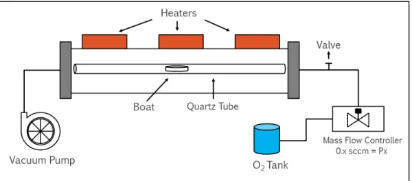
Methods
We use a three part furnace made by Protherm that can reach to 1050 ◦C. V2O5 fine powder used as precursor, which is placed in an Alumina boat. The substrate
sits above the Alumina boat with roughly 1 cm apart the precursor, this set up is made to minimize the differences of vapor flux coming from the precursor. For all growths except sapphire, 20(±3) mg precursor is used, for sapphire 10(±1) mg is used; the reason being that 10mg is enough to cover all of the surface of the sapphire surface while for Si, SiO2 and Quartz substrates 20mg precursor gave
better coverage. The growth is divided to two parts, a heat up period and growth period. In the heat up period the furnace is brought to the target temperature in 20±2 minutes, while giving a predetermined oxygen flow under vacuum.
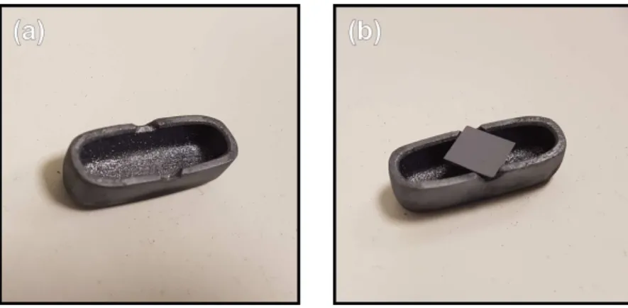
Figure 2.4: Alumina boat used in the growth a) Both sides of the boat is dented to acommodate a 1cm x 1 cm substrate. b) boat-substrate arrangement, substrate stays upside down so that the growth surface directly faces the precursor with roughly 1 cm distance. The alumina boat and the quartz tube acquires a black color after repeated VO2 growths, but this has no effect on the growth itself and
all of our results are repeatable with clean boat and tube.
The amount of oxygen during the heat-up period changes the mode of growth and the Oxygen flow coded as ‘Px’ which refers to ‘x times 0.1 sccm flow rate’. So P5 refers to 0.5 sccm oxygen flow in the heat up period and P3 refers to 0.3sccm and P500 is 50 sccm and so on. The growth types are labeled with centigrades temperature in the front and the flow rate near it. For example in ‘780-P5’ growth, 0.5 sccm Oxygen is given to system in the heat up period and after reaching to growth temperature of 780 ◦C the flow is ceased. All of the growth is done under vacuum which creates 10−2 mbar pressure environment. We use ALICAT SCIENTIFIC brand with MC-100SCCM-D/5M model as our flow controller, and the pressure is measured with Pfeiffer Compact FullRange
Gauge. The pressure values at 750 oC were, P 0 = 1.5x10⁻²mbar P 1 = 2.6x10⁻²mbar P 2 = 3.1x10⁻²mbar P 3 = 3.5x10⁻²mbar P 4 = 3.9x10⁻²mbar P 5 = 4.3x10⁻²mbar
Another important thing to consider was that the VO2growth is very sensitive to oxygen presence in the system so another valve was added at the end of the flow controller in order to seal off the growth chamber after the heat up period. There is a very low amount of leakage that comes from the flow controller which interferes with the VO2 growth. At the end of the heat up period, the flow is
closed and then the valve is closed, then the pressure drops to 10−2 mbar in around 30 minutes.
If not specified differently, the growth period time is always chosen as 90 minutes. The substrates are cut with 1 cm x 1 cm dimension then wiped with a tissue wetted with isopropanol and then washed with acetone, isoproponal and D.I. water in that order. Lastly remaining liquids are blown away with N2 gun.
2.0.3
SiO
2substrate
For these experiments we have used single crystal (100) Si wafers covered with a 1µm thick, thermally grown SiO2 layer. At heat up period, precursor melts and starts to have vapour pressure around 680 ◦C [2]. The vapour coming from the precursor condense on the surface of the substrate and makes V2O5domes as
mentioned before. VO2 crystals doesn’t grow out of these in an instant especially
if oxygen is present in the heat up period. To observe the crystal growth stages, four different samples were prepared using 750-P3 route in which the growth stopped and the system was rapidly cooled at different times after the start of
crystal growth period. As it can be seen from the Figure 2.5, the process takes more than 50 minutes. Figure 2.6 shows XPS graphs which support this claim, at 10 minute and 30 minute marks the +4 phase peak which indicates VO2 presence is not visible.
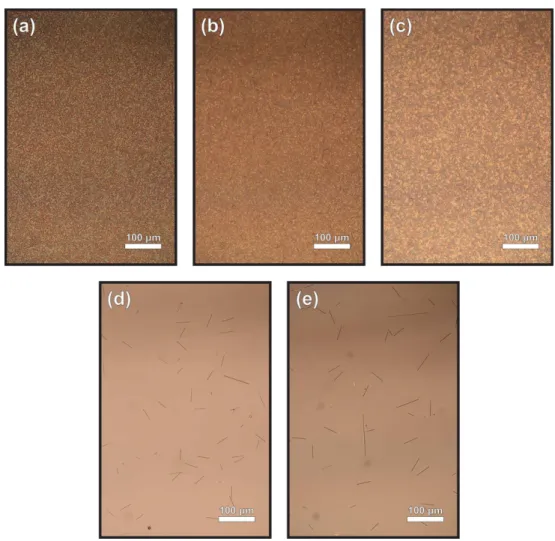
Figure 2.5: Optical microscope images of 750-P3 route stopped at certain times after the start of crystal growth period. Three different samples are prepared which show different moments of growth; a) 10 minutes, b) 30 minutes, c) 50 minutes after the start of crystal growth period.
Figure 2.6: XPS analysis of four different samples prepared with 750-P3 route which were stopped at a) 10 minutes, b) 30 minutes, c) 50 minutes d) 90 minutes after the crystal growth period. The O1s peaks are The +4 phase peak from VO2 doesn’t occur after 10 minutes and 30 minutes. Vanadium +5 phase peak coming from The V2O5 persist even after 90 minutes due to thin layer of oxidation on
the surface of the crystals. The references used for the analysis are: [3][4][5].
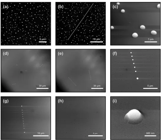
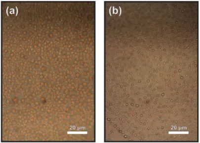
Figure 2.7 shows the Scanning Electron Microscope images of the growths that has been stopped after 15 minutes into the ceasation of oxygen flow at 780 ◦C. When we consider 300nm and above sized dome amounts per area between P2 and P3 routes we see a huge difference. Obviously the critical radius (the radius required for a stable and growing cluster of atoms) required for domes to get larger for P2 is smaller than P3 which helped the domes to get bigger in lesser time compared to P3. We used imageJ software to calculate the diameters of the domes. The silver colored domes in P2 were around 300-446 nm in diameter while P3 silver colored domes were between 400-600nm. The grey domes of P3 were
between 100-200nm. The silver domes connect and start to create line clusters, the lines connecting them are visible under SEM. When we compare P3 and P5, nucleation rate doesn’t seem very different but our observation was when we consider connected domes, P3 had larger amount of the low number (2, 3, 4) dome cluster lines compared to P5. In P5 the line clusters mainly had more than 5-6 domes in them. Overall P3 had more line clusters. This may be resulting from line clusters with fewer domes having a harder time to connect and grow at P5. The silver domes of P5 were between 650-790nm in diameter and grey domes were around 160-300nm. Our conclusion is that as more oxygen is in the system during the heat-up period the critical radius of domes also increase.
Figure 2.7: Electron microscope pictures of the growths that has been stopped after 15 minutes into the ceasation of oxygen flow at 780 ◦C. (a), (b), (c) are pictures of P2-780 method. The nucleation rate is pretty high and the domes connect as they come together. The connection lines can be seen at (c). (d), (e), (f) are the images of P3-780 method. The nucleations are much more scarce compared to P2-780. (g), (h), (i) are images of P5-780 method. The nucleation rate is not that much lower than P3-780 but domes that are connected are more scarce.
We have conducted experiments of crystal growth at 720 ◦C, 750 ◦C, 780◦C and 830◦C with changing oxygen flow values at the heat up period. The Si/SiO2
substrate surface starts to lose oxygen at temperatures as low as 720 ◦C under vacuum and without any oxygen flow. However at 720 ◦C with oxygen flow of P2 at heat up period prevents the loss of oxygen of the SiO2surface. This makes the surface have higher oxygen concentration which prevents the V2O5 domes to
pass its oxygen to the substrate. The result is the suppression of most of the nucleation of VO2 crystals.
Figure 2.8: With no oxygen flow during the heat up period the SiO2surface starts to lose its oxygen and takes oxygen from V2O5 domes, starting the nucleation. (a) shows the schematics of this process with (b) showing the optical image of the result, substrate surface fully covered by VO2. When there is 0.2 sccm O2
flow during the heat up period, surface of the SiO2 substrate doesn’t lose a lot
of oxygen and in turn V2O5 domes have much lower nucleation rate. (c) shows
the schematics of this process and (d) shows the optical image of the result, the domes mostly stay intact without turning to VO2. The temperature during the growth period was 720oC for both cases
In all of our experiments from 750 ◦C to 830 ◦C, with the increase in oxygen flow at heat up period, a transition from platelet to rod shape happens and nucleation rate drops drastically. For every temperature between 750◦C and 830
◦C we get thin platelets at P3 and below oxygen flow values, while it has rod
increase. The white-grey color indicates that the crystal is over 200nm thickness and other colors like red, yellow and blue indicates they are thinner than roughly 170 nm. We also see that compared to P0 or P2, P3 results with larger grain size. The optical images of the mentioned results can be seen below, in figures 2.9, 2.10 and 2.11.
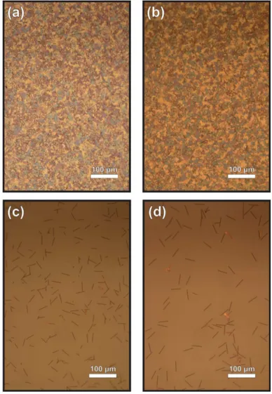
Figure 2.9: Optical images of growth at 750 ◦C with a) P0, b) P2, c) P3, d) P4 e) P5 routes.
Figure 2.10: Optical images of growth at 780 ◦C with a) P2, b) P3, c) P4 d) P5 routes.
Figure 2.11: Optical images of growth at 830◦C with a) P3, b) P4, c) P5 routes.
The reason of this can’t be explained by different deposition rates of the precursor at different oxygen flow values, since the dome density doesn’t seem to change with different oxygen flow values. Result of one experiment can be seen in Figure-2.12 where 750-P3 and 750-P5 routes of growth were stopped 10 minutes after the start of the crystal growth period; and the substrates were examined under optical microscope. There seem to be no major difference between dome densities and their radius.
Figure 2.12: Optical images of a) 750-P3 b) 750-P5 routes, the growths were stopped 10 minutes after the start of the crystal growth period.
We argue that the reason of different crystal morphology is due to SiO2surface
having different oxygen levels at different flow rates which in turn changes the nucleation rate and catalytic potency. If the oxygen level on the substrate surface is low, it is easier for the precursor to lose its oxygen so nucleation rate increases. Due to a mix of the effects of many domes getting connected via growing crystal rods and high chemical potency, we get thin and low aspect ratio crystals and all the surface is covered. When the oxygen level is P4 or high, the surface of the silica substrate is mildly lacking oxygen so it reacts with only a small amount of the V2O5 domes thus most of the precursor domes evaporates without forming a crystal. The coverage of the surface is minimal and the preferred growth shape is nanorods. This change is very drastic and the flow change is only 0.1 sccm. At 750 ◦C, with P3 oxygen flow the oxygen partial pressure is 1.9-2.0x10⁻² and with P4 it is 2.3-2.4x10⁻² mbar.
Our hypothetic model is as follows. If the Oxygen value is low enough at heat up period the surface of SiO2loses its oxygen and can take the oxygen of the V2O5
domes. However at certain oxygen partial pressures for the temperatures between 750-830◦C, the oxygen can’t leave SiO2 surface effectively so that the nucleation
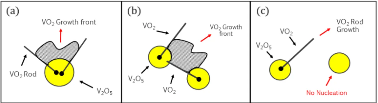
rate of domes are very low due to lack of catalytic effect from the substrate. When the nucleation rate is high, almost all of the domes create one and maybe more than one rod nucleations. If one dome has two different rods growing out of it, it may create a suitable bed for two dimensional growth in between the two rods as shown in Figure 2.13(a). This is a result of the precursor wetting the VO2surface
as mentioned in Figure 2.1. Another possibility is that when almost all of the the domes nucleate, the VO2rods can connect with other domes, which creates a growth front in between the rods of these two domes, as shown in Figure 2.13(b). When the nucleation rate is low the domes cannot be connected by rods due to very low possibility of two domes side by side nucleating at the same time. Also the chance of one dome making two rods are almost impossible. This process is shown in Figure 2.13(c).
Figure 2.13: Schematics of proposed dynamics of different morphologies seen in VO2 growth for temperatures between 750-830 ◦C. (a),(b) shows the x≤3 of Px
route where VO2 platelets cover the surface. (c) shows x > 3 where no platelets
are seen and the surface is covered with VO2 rods.
2.0.4
VO
2growth Methods
As mentioned before for the Hall Effect measurement project, large VO2 crystals
with low aspect ratio was needed. The problem with the growth of P3 and under is that the nucleation rate is so high that the crystals form a continuous layer on the substrate and it is impossible to remove them using a simple needle-manipulator system shown in Figure-2.18. Above P3 however we get one dimensional rods with very high aspect ratio. With the light of the experiments we performed on Si/SiO2 substrate, we came up with two methods. In Method-1, we tried to
increase the nucleation rate using the heating elements of the furnace. where the chamber was heated to 790◦C under vacuum and 0.5 sccm O2flow. The pressure
stays around ∼ 6x10⁻² mbar during the heat up period. After reaching to 790◦C the flow was ceased so that the pressure is around ∼ 1x10⁻² mbar and then the furnace is heated to 950 ◦C in 32 mins, in other words 5 ◦Cmin−1 heating rate. The idea is that due to the radiation coming from the furnace, top surface of the precursor droplets would be heated higher than the ambient temperature so that they would nucleate at a higher rate. We had moderate amount of success with creating around 40-60 nm platelet crystals with around 20 µm length but we were unable to remove them physically from the surface of the growth substrate so we didn’t investigate more about it. When the crystals are very thin, to remove them
from surface intact other methods like removing with the help of polycarbonate should be used. But the thinness of the crystal might be quite valuable for the TEM studies. Figure-2.14 shows a sample made using Method-1 growth.
Figure 2.14: Optical image of Method-1 growth on SiO2 substrate. During the time that the system was reaching to 790 ◦C, 0.5 sccm O2 flow given to system. The flow was ceased at 790 ◦C so while the furnace is heated to 950 ◦C with a heating rate of 5 ◦Cmin−1.
In Method-2, We used micro scale particles that would increase the chances of nucleation where they are present, acting as heterogenous nucleation zones. At P5, this results with some precursor domes nucleating very early and connecting other domes before they evaporate, so we get large crystals due to, we believe, the dynamics shown in figure 2.13(b). These crystals are also not connected as in P3 so instead of a polycrystalline film we get large, seperate, single crystal VO2 beams.
We used a nitrile glove to crete these micro scale particles. After cleaning the SiO2 substrate, the surface is pressed by the finger of glove which resulted with many particles on the surface. However a certain size and/or number per area is needed to have this effect uniformly so that only one in five-ten growth resulted with high amount of large crystals everywhere on the substrate. On the other hand a good growth can provide around thirty to fifty crystals easily. The foreign
particles don’t seem to affect the crystal quality due to VO2 crystals not showing
any difference of MIT temperature and showing very well shaped facets. The TEM results can be seen in the next section where the electron diffraction patterns show single crystal nature of the resulting crystals from this type of growth. And from our experiments, 780-P5 route seem to be the optimum method to grow thin and low-aspect ratio crystals. The crystal thickness was in general between 75nm-170nm. Higher oxygen value during the heat up period or higher temperature at crystal growth period results with thicker crystals. Lower temperature at crystal growth period decreases the amount of platelets and creates higher aspect ratio crystals. This type of Method-2 growth can be seen in figure 2.15.
Figure 2.15: Optical microscope image of crystals grown on 1 µm SiO2 substrate
Figure 2.16: Schematics for (a) Method-1 where the radiation coming from the heaters is utilized and (b) Method-2 where particles coming from the nitrile glove are utilized to increase the rate of nucleation and the size of crystals.
All the VO2crystals used in the applications mentioned in this thesis are grown on 1µm SiO2 substrate using Method-2 with 780-P5 route. These crystals were
also routinely utilized for another project in our group where the crystals were transferred on top of exfoliated h-BN flakes. h-BN flakes were exfoliated on 1µm SiO2 substrates.
Figure 2.17: Optical microscope images of various crystals grown using Method-2 with 780-P5 route transferred onto hBN flakes for the use in hall-effect measurement devices. Scale bar is 20 µm.
These crystals were transferred using a micro manipulator system. After the growth, the substrates were dipped to buffered hydrofluoric acid (BOE 7:1 (HF : NH4F = 12.5 : 87.5%) for two minutes to ease taking up the crystals using tungsten needle with 1µm diameter tip attached to micro manipulator. BOE etches the SiO2 but doesn’t etch away VO2. The micro manipulator system with
tungsten needle holder attachment shown in figure 2.18.
Figure 2.18: Micro manipulator with tungsten needle tip. All of the VO2crystals are removed from the surface and transferred using this system. To ease the removing of the crystals from the surface of SiO2 substrate, the substrates are
dipped into 1:7 BOE solution for 2 minutes. If necessary this step is repeated.
2.0.5
Si substrate
We used single crystal <111> oriented p-type(boron as dopant) silicon wafers in these experiments. The catalytic effect of the substrate is much higher in single crystal Si substrates case because of large O2 affinity of the substrate. With this
substrate we observed that the nucleation rate stays high even at P500 growth, but with higher oxygen the thickness of the crystals increase and they become
more three dimensional. We claim that high rates of nucleation at high oxygen levels is due to the diffusion of oxygen from V2O5to the layers under the substrate which means the eutectic layer must be thicker than the oxygenated surface of the Si substrate. But we can effectively nullify the catalytic potency of substrate surface (not the bulk) so that P500 during the heat up period results with the VO2
crystals not forming platelets but acquiring three dimensional shapes instead, in line with Wulff-Kaischew theorem.
Figure 2.19: Optical microscope image of growth of silicon wafer at 780 ◦C with a) P5, b) P500 routes.
Figure 2.20: Electron Microscope image of growth on silicon wafer at 780◦C with a) P5, b) P500 routes. P5 route shows low aspect ratio thin platelets while P500 shows three dimensional shapes due to low chemical potency of the surface.
2.0.6
Quartz substrate
Opposite of the Si substrate, here the catalytic effect is very low so the nucleation rate is also low. Without oxygen flow the surface is fully covered with VO2but P2 route at 780◦C is enough to suppress the nucleation. Given the same temperature and oxygen levels, chemical potency of Si substrate is highest and Quartz lowest with 1µm SiO2 substrate in between.
Figure 2.21: Growth on Quartz substrate at 780 ◦C with a) P0, b) P2 routes.
2.0.7
Sapphire c-plane
Similar to SiO2 case, supplying oxygen to system at heating period results with lesser nucleation rate. This is probably due to similar mechanisms of growth; in sapphire case there might be a similar reaction that takes place between the surface and the precursor which latter donating its oxygen to the substrate. On the other hand there is an epitaxial relationship between VO2
and the sapphire surface. V2O5 also accumulates on the surface with an ordered
structure which might imply another epitaxial relationship. Oxygen provided to system is considerably more than SiO2 case, mostly between 1-7 mbar partial pressure during the heat up period. When the growth is done under the vacuum
at 750 ◦C, the surface of the substrate is covered with tiny crystals that are generally not connected to each other. This result is probably the result of two things, slow crystal growth and high nucleation rate. We would expect the same morphology at temperatures between 750-850 ◦C but we don’t have records for other temperatures. When oxygen is supplied during heat up period, the density of nucleation sites decrease but the length of the crystals grow considerably, which can be seen in figure 2.22 (b).
Interestingly, if the temperature is raised during the growth period(Method-1), we get the best results. Increasing temperature during the growth most likely raises the supersaturation of the V2O5domes on the substrate by heating them to
a higher temperature compared to the growth period temperature. So the V2O5
domes nucleate faster but the temperature most likely becomes same with the system at the time of crystal growth. The result is that the nucleation rate is enhanced and nucleation occurs earlier compared to the 850-P5 route. This results with crystallization also beginning earlier so that a larger amount of precursor turns to VO2 instead of evaporating as in 850-P5 route.
Figure 2.22: Optical microscope image of VO2 on c-cut sapphire. (a) No oxygen
flow given to system at heat up period and the temperature was 750◦C at growth period, (b) 1:3 O2:Ar flow provided to the chamber during the heat up period
and c) 1:3 O2:Ar flow provided to the chamber during the heat up period till 750
We also observed Vertical growth of VO2 with many different morphologies
using Method-1 with Sapphire c-plane substrates. Sohn and colleauges showed in their work that the vertical growth of VO2 is seen on a-cut and r-cut sapphire but not on c-plane [46]. Because they grow in certain places and considering the results of a-plane and r-plane we came to conclusion that they occur because of existing steps on the substrate. This suggests that with different miscuts on c-plane we can get different morphologies of vertical VO2 crystals. These growths
can be seen in figures 2.23 and 2.24.
Figure 2.23: Different modes of growth under optical microscope, with VO2beams and vertical rods. Vertical rods cast shadows on the substrate.
Figure 2.24: Different morphologies of VO2 under electron microscope that were
grown on sapphire c-plane substrate. All the scalebars are 20µm.
Both are seem to be epitaxial growth of VO2, similar to the growths reported
by Sohn and colleagues [46]. As layed out in Sohn et al’s work the epitaxial relation between VO2 and c-cut sapphire is (010) VO2//(0001) sapphire and our XRD measurement shows that our growth has 39.9◦ (020) and 85.9◦(040) signals of VO2. The indexing is done using Pearson’s Crystal Data.
Figure 2.25: XRD results for VO2 growth on c-cut sapphire. During the heat
up period a growth 1:3 O2:Ar flow provided to the chamber till 750 ◦C then
Chapter 3
TEM Studies of Hydrogen Doped
Crystals
The metal-insulator transition of VO2 crystals can be modified by atomic hydrogen Doping using catalytic spillover method. At temperatures above 65
◦C, atomic hydrogen enters from the tip of the crystal which is [001] direction
of the rutile phase [37]. The hydrogen atom can only enter through the lattice openings that exist only in the (001) plane of the rutile phase of the crystal.
As Chippindale and his colleagues demonstrated in a 1991 study, this results with MIT disappearing from the system with another metallic system staying thermodinamically stable at room temperatures. They mention doping is quite slow under 90 ◦C and improves significantly after that value which we also observed. These doped compounds which referred as HxVO2, changes its crystal
structure with changing x values. Between 0 ≤ x ≤ 0.08 it stays at monoclinic phase but for values x>0.08 the crystal structure becomes orthorombic and lattice parameters change with differing x values[40]. Filinchuk et al. further improves this with dividing the orthorombic structures to two phases, O1 and O2, O1 being the phase not having ordered hydrogen positions and O2 being the one with ordered hydrogen positions[39].
Figure 3.1: The monoclinic (M1), tetragonal-rutile (R) and orthorhombic (O1) structures of VO2 are shown, looking from the c-axis for R, O1 structures
and slightly misaligned a+c direction for M1. Oxygen atoms are colored red and Vanadium atoms are colored grey. Below the transition temperature, VO2
crystal has monoclinic(M1) structure and above it has rutile(R) structure. With hydrogen doping the lattice structure turns into orthorombic structure with ‘b’ lattice constant of rutile structure getting larger. Reprinted (adapted) with permission from (Filinchuk, Yaroslav, et al. ”In situ diffraction study of catalytic hydrogenation of VO2: Stable phases and origins of metallicity.” Journal of the American Chemical Society 136.22 (2014): 8100-8109). Copyright (2014) American Chemical Society.
As the HxVO2 crystal receives more hydrogen, the O1 phase turns into O2.
O1 phase has Pnnm space group with lattice constants a = 4.4795(12), b = 4.7372(11), and c = 2.8944(5) ˚A, compared to VO2(R), the b lattice constant is larger(b=4.554˚A for the rutile phase). O2 phase has Fdd2 space group with