DEVELOPMENT OF PHOTOANODES
FOR PERFORMANCE ENHANCED DYE
SENSITIZED SOLAR CELLS
A THESIS SUBMITTED TO
THE GRADUATE SCHOOL OF ENGINEERING AND SCIENCE
OF BILKENT UNIVERSITY
IN PARTIAL FULFILLMENT OF THE REQUIREMENTS
FOR THE DEGREE OF
MASTER OF SCIENCE
IN
MATERIALS SCIENCE AND NANOTECHNOLOGY
By
Türkan Gamze Ulusoy
ii
DEVELOPMENT OF PHOTOANODES FOR PERFORMANCE ENHANCED DYE SENSITIZED SOLAR CELLS
By Turkan Gamze Ulusoy
August, 2015
We certify that we have read this thesis and that in our opinion it is fully adequate, in scope and in quality, as a thesis for the degree of Master of Science.
Assist. Prof. Dr. Ali Kemal Okyay (Advisor)
Prof. Dr. Ahmet Macit Özenbaş
Assist. Prof. Dr. Ferdi Karadaş
Approved for the Graduate School of Engineering and Science:
Prof. Dr. Levent Onural Director of the Graduate School
iii
ABSTRACT
DEVELOPMENT OF PHOTOANODES FOR
PERFORMANCE ENHANCED DYE SENSITIZED
SOLAR CELLS
Türkan Gamze Ulusoy
M.S in Materials Science and Nanotechnology
Advisor: Assist. Prof. Dr. Ali Kemal Okyay
August, 2015
With a raising demand for clean and renewable energy sources in recent decades, dye sensitized solar cell (DSSC), as an efficient and low-cost solar cell technology, have attracted considerable attention and several efforts have been directed for the optimization of all components of DSSCs including photoanode, sensitizer dye, hole transport layer and counter electrode. The objective of this thesis is to provide a better understanding on the function of photoanode in overall performance of DSSC device by highlighting problems and limitations and offering proper solutions to tackle these deficiencies. Based on this understanding, this thesis reports, fabrication, characterization and analysis of designed three different cells to boost device photovoltaic performance which includes: 1) angstrom thick ZnO-sheathed TiO2 nanowires
as photoanodes, 2) multifunctional omnidirectional antireflective coating, 3) peptide nanofiber network templated ALD-grown TiO2 nanostructures as
photoanodes in DSSC.
Since photoanode-dye interface engineering is of utmost importance, the first of our proposals in this thesis relies on a systematic approach to understand the impact of atomic layer deposited (ALD) angstrom-thick ZnO sheath on hydrothermally grown TiO2 nanowires (NWs) core utilized as photoanodes in
iv
efficiency enhancement almost three times via reducing recombination rate of injected electrons, enhancement in collection efficiency of electrons via reducing density of surface trap states without hampering injection efficiency and increased dye uptake on TiO2 nanowires’ surface which in turn leads to
increased light absorption.
On the other work, we also utilized multifunctional organically modified silica (ORMOSIL) as antireflection coating layer on DSSC to improve conversion efficiency of the device via reduction in the light reflection. ORMOSIL coated DSSC surfaces show a low-reflective omnidirectional response in a wide range of wavelengths (400-800 nm). At normal incidence (𝜃=0°), the short circuit current density (JSC) is improved to an amount of 23% as a result of ORMOSIL coating. In addition, JSC meets even higher amounts of enhancement where 84% increase is recorded at 𝜃=30°. Moreover, this coating exhibits superhydrophobicity representing a contact angle of 155º.
Finally, we proposed and implemented, self-assembled peptide amphiphiles nanofiber 3D networks in order to obtain TiO2 nanotube structures as a
template in DSSC. These self-assembled peptide amphiphiles are resistant to high temperature and more durable than other kinds of peptide amphiphiles. The advantage of this 3D fiber composed template is its high surface area and interconnected solid support providing an effective template for formation of TiO2 network using ALD. On the other hand, since ALD offers uniform and
conformal coating of high aspect ratio features, it ensures an ideal thin film coating method on high surface area nano-template materials such as the peptide nanofiber templates proposed in this study.
Keywords: Photovoltaics, dye sensitized solar cells (DSSCs), interface engineering, atomic layer deposition (ALD), metal-oxides, zinc oxide, titanium dioxide, antireflection coating, peptide template, nanofiber.
v
ÖZET
YÜKSEK VERİMLİ BOYA UYARIMLI GÜNEŞ
PİLLERİ İÇİN FOTOANOT GELİŞTİRİLMESİ
Türkan Gamze Ulusoy
Malzeme Bilimi ve Nanoteknoloji, Yüksek Lisans
Tez Danışmanı: Yrd. Doç. Dr. Ali Kemal Okyay
Ağustos, 2015
Yenilenebilir ve temiz enerji kaynaklarına son yıllarda verilen önem, boya
uyarımlı güneş pillerine (DSSCs) yoğun ilgiyi beraberinde getirmiş ve bu
aygıtların yapısında bulunan fotoanot, aktifleştirici boya, boşluk (hole) aktarım katmanı ve karşıt elektrot gibi bileşenlerin yüksek performans için optimize edilmesine sebep olmuştur. Bu çalışmada, fotoanot bileşeninin DSSC performansına nasıl etki ettiği, aygıt çalışmasında ortaya çıkan sorunlar ve kısıtlamalar ele alınarak incelenmiş ve bu sorunlar için geliştirilen çareler sunulmuştur. Yapılan çalışmalar sonucunda ise DSSClerin fotovoltaik performansını arttırmak için üç farklı yöntem kullanılmıştır. Bu tezde fotoanot olarak 1) angstrom kalınlığında ZnO-kaplı TiO2 nanoteller, 2) çok-işlevli, her
açıdan geri yansıtmasız kaplamalar ve 3) peptit nanofiber alttaşı kullanılarak ALD ile büyütülen TiO2 nanotüpler olmak üzere DSSC sistemleri için
geliştirilen performans-arttırıcı fotoanot yapıların sentezi, karakterizasyonu ve analizi detaylandırılmıştır.
Fotoanot ve boya katmanları arasında bulunan arayüzeyin optimizasyonu, fotoanot performansı için hayati önem taşımaktadır, dolayısıyla bu tezdeki ilk sunulan çalışmada hidrotermal yöntemi ile büyütülmüş TiO2 nanotellerin
üzerine angstrom kalınlığında ZnO tabakası atomik katman kaplama (ALD) tekniği ile kaplanmış ve fotoanot olarak DSSClerde kullanılmasının etkisi incelenmiştir. Angstrom kalınlığındaki ZnO katmanı, TiO2 nanoteller için bir
vi
arayüzey görevi görmektedir. Elde edilen sonuçlar, bu süper-ince katmanın cihazın verimini, (a) sistemdeki elektronların boşluklarla yeniden birleşmesini engelleyerek, (b) elektron enjeksiyonuna engel olmadan nanotellerin yüzeydeki kusur yoğunluğunu azaltıp elektronları toplama verimini arttırarak ve (c) TiO2 nanotellerin yüzeylerinde boyanın emilimini güçlendirerek
absorplanan ışık miktarını arttırarak verimin neredeyse üç kat arttıracağını göstermiştir.
Diğer bir çalışmada ise; organik olarak modifiye edilmiş silika (ORMOSIL) DSSClerde çok işlevli bir yansıma engelleyici katman olarak kullanılmış, ışık yansıması engellenerek cihazın enerji üretim verimi arttırılmıştır. ORMOSIL kaplı DSSC yüzeyleri, her açıdan ve geniş bir dalgaboyu aralığından (400-800 nm) gelen ışığın yansımasına engel olmaktadır. Bu kaplama sonucunda, kısa devre akım yoğunluğu 0 dereceden gelen (normal) ışık için %23 artmış ve 30 derecelik bir açıda %84’e kadar çıkmıştır. Ayrıca, ORMOSIL kaplaması 155 derecelik bir temas açısına sahiptir ve dolayısıyla süperhidrofobik özellik göstermektedir.
Son olarak, kendiliğinden birleşme (self-assembly) yardımı ile üç boyutlu yapılar oluşturan peptit amfifil nanofiberlerinin kalıp olarak kullanımı ile TiO2
nanotüplerin sentezlenmesi gösterilmiştir. Kullanılan peptit nanofiberler, geleneksel peptit yapılarına göre yüksek sıcaklıklarda daha dayanıklıdır. Düşük çaplara sahip olan bu fiberler tarafından oluşturulan üçboyutlu yapılar, yüksek yüzey alanlarına sahip olup, birbirine bağlı TiO2 nanotüp yapılarının
oluşturulması için etkili bir ALD kalıbı olarak işlev görmektedir. ALD, nanofiber yapılarının üniform ve yüzeyi tutarlı bir şekilde takip edecek şekilde kaplanmasını sağladığından bahsi geçen en/boy oranı yüksek peptit yapılarını kaplamak için ideal bir yöntemdir ve bu yüzden kullanılmıştır.
Anahtar kelimeler: Fotovoltaik, boya uyarımlı güneş pilleri (DSSCs), yüzey mühendisliği, atomik katman kaplama (ALD), metal oksitler, çinko oksit, titanyum dioksit geri yansitmasiz kaplama, peptit alttaşı, nanofiber.
vii
Be less curious about people and more curious about ideas.
Marie Curie
viii
ACKNOWLEDGEMENT
First and foremost I wish to thank my supervisor, Assist. Prof. Dr. Ali Kemal Okyay, for giving me the opportunity to occupy all the facilities and his invaluable academically and emotionally contributions throughout my entire graduate studies. He normally has a very busy schedule, but he would always find time to discuss my research progress. On the verge of finishing my master degree, I am so grateful for working with such an advisor within this field.
I would also like to say special thanks to Assist Prof. Ferdi Karadas and Prof. Ahmet Macit Özenbaş for attending my thesis committee.
It is a great pleasure to acknowledge all the professors, instructors, engineers, and graduate students at UNAM Materials Science and Nanotechnology Department. Also, I would like to thank to UNAM administration office and Ayşegul Torun, for their attention and favor during my graduation. I must also thank Nimet Kaya who helped me overcome many crisis situations at dormitory.
I gratefully acknowledge financial support by TÜBITAK (The Scientific and Technological Research Council of Turkey) under the project name BIDEP 2210-C M.Sc. fellowship.
Also, I express my heartfelt thanks to my undergraduate research advisors, Prof. Dr. Zeki Aktaş and Assoc. Prof. Dr. Emine Yağmur, from Chemical Engineering Department of Ankara University for their illuminating and friendly guidance, constructive criticism on various issues in my personally and academic life since the day I began my research as an undergraduate.
My sincere thanks also go to Assist Prof. Kağan Topallı for his insightful comments and encouragement in all the time of my study.
I am deeply thankful to my group members for providing an honest and friendly environment. Thank you to those who are my laboratory colleagues and fellows Kerem Çağatay İçli, Kinyas Polat, Tuna Demirbas, Ruslan
ix
Garifullin, Bihter Dağlar, Sahin Beşerik, Hamit Eren, Zeliha Soran-Erdem, Talha Erdem, Yusuf Keleştemur, Fatma Kayacı, Yelda Ertaş, Aslı Çelebioğlu, Arif Khalily and Shahab Akhavan for always being kind, helpful and friendly. I want to acknowledge and appreciate their moral support, patience and kindness during my research. I owe my deepest gratitude to my dearest friends Nuray Gündüz, Pelin İşgor, Şeyma Canık, Burak Güzeltürk and Yildiz Gozde Sağlam for their help and transparency. I will never forget the awesome time we have had together and I feel very lucky to get to know such great people.
I feel the need to single out Amir Ghobadi, for his professional support valued, from whom I have learned many things and he never fed up to help me from the beginning to the end. I would not have been able to accomplish this task without his scientific knowledge, enthusiasm, experience and invaluable support.
And finally, without a doubt most importantly, I would like to thank my parents Şerife and Hakan, my siblings İpek and Emre, my aunt Şaziye and my uncle Mustafa for their sacrifices, understanding, patience and countless support all the time. I feel exceedingly lucky to have had these people in my life.
x
CONTENTS
ABSTRACT……...………...………...
IIIÖZET……...………...………...
VA
CKNOWLEDGEMENT……...………...……….
VIIIL
IST OFF
IGURES……….…..
XIIIL
IST OFT
ABLES…..………..………...
XVIIIC
HAPTER1
I
NTRODUCTION... …1
1.1 MOTIVATION OF THE THESIS ... 3
1.2 ORGANIZATION OF THE THESIS... 3
C
HAPTER2
S
CIENTIFICB
ACKGROUND... 5
2.1 INTRODUCTION TO DYE SENSITIZED SOLAR CELLS (DSSCS) ... 5
2.1.1 DSSCINSPIRED BY PHOTOSYNTHESIS………5
2.1.2 ADVANTAGES OF DSSC……….7
2.2 BASIC STRUCTURE OF DSSC……….9
2.2.1 TRANSPARENT CONDUCTIVE OXIDE SUBSTRATE………...9
2.2.2 SEMICONDUCTOR PHOTOANODE………...10
2.2.3 DYE SENSITIZER………11
2.2.4 ELECTROLYTE………13
2.2.5 COUNTER ELECTRODE………...13
2.3 ELECTRON TRANSFER DYNAMICS OF DSSCS………...14
xi
3.1 MATERIAL CHARACTERIZATION ... 19
3.2 PHOTOVOLTAIC PERFORMANCE CHARACTERIZATION…………19
3.2.1 CURRENT-VOLTAGE (I-V)MEASUREMENT………..20
3.2.2 INCIDENT PHOTON TO-CURRENT CONVERSION EFFICIENCY (IPCE)………..21
3.3 TIME-RESOLVED TRANSIENT CHARACTERIZATION ... 22
3.3.1 TRANSIENT OPEN CIRCUIT PHOTOVOLTAGE DECAY MEASUREMENT……….23
3.3.2 TIME RESOLVED PHOTOLUMINESCENCE DECAY SPECTROSCOPY ………..23
3.4 OPTICAL CHARACTERIZATION ... …24
3.4.1 PHOTOLUMINESCENCE MEASUREMENTS………..24
3.4.2 UV-VIS-NIRABSORPTION………..25
C
HAPTER4
S
URFACEE
NGINEEREDA
NGSTROMT
HICKZ
NO
S
HEATHEDT
IO
2N
ANOWIRES ASP
HOTOANODE INDSSC ... 26
4.1 INTRODUCTION ... 26
4.2 MATERIALS AND REAGENTS ... 28
4.3 SYNTHESIS OF TIO2NANOWIRES ... 28
4.4 ALDDEPOSITION ... 29
4.5 DEVICE ASSEMBLY ... 29
xii
C
HAPTER5
O
MNIDIRECTIONALA
NTIREFLECTIVEC
OATINGSFOR
P
ERFORMANCEE
NHANCEDDSSC ... 48
5.1 INTRODUCTION ... 48
5.2 MATERIALS AND REAGENTS ... 50
5.3 PREPARATION OF NANOPOROUS ORMOSILCOATINGS ... 50
5.4 PREPARATION OF NONPOROUS ORMOSILCOATINGS ... 51
5.5 PREPARATION OF THREE-LAYER COATING ... 51
5.6 DSSCASSEMBLING ... 52
5.7 RESULTS AND DISCUSSIONS ... 52
C
HAPTER6
P
EPTIDEN
ANOFIBERN
ETWORKT
EMPLATEDALD-GROWN
T
IO
2N
ANOSTRUCTURES FORDSSC ... 59
6.1 INTRODUCTION ... 59
6.2 MATERIALS AND REAGENTS ... 60
6.3 SYNTHESIS OF PEPTIDE FOR 3DTIO2NANONETWORKS ………..60
6.4 PHOTOANODE FABRICATION ... 61
6.5 DSSCASSEMBLING ... 62
6.6 RESULTS AND DISCUSSION ... 62
C
HAPTER7
C
ONCLUSIONS... 69
7.1 KEY CHALLENGES AND RECOMMENDATIONS ... 70
7.2 CONTRIBUTIONS ... 71
xiii
LIST OF FIGURES
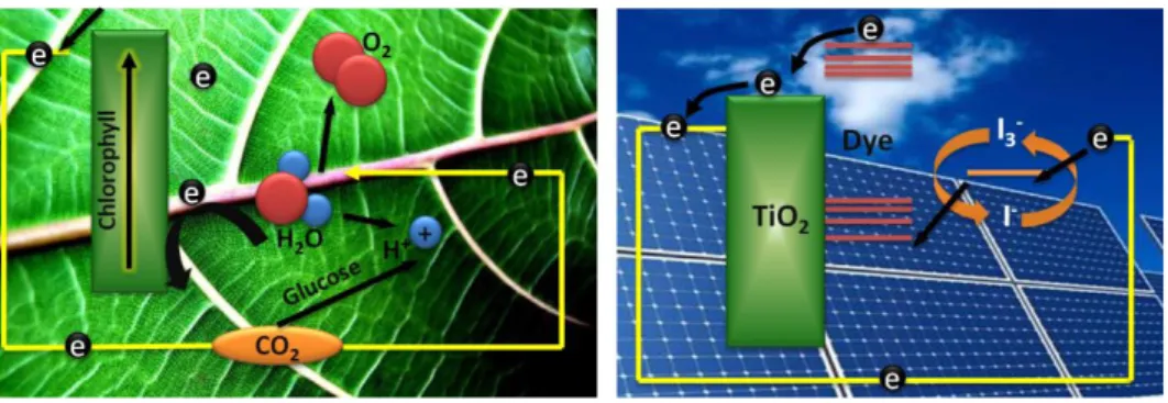
Figure 2.1: Light conversion analogy between photosynthesis and dye
sensitized solar cell (DSSC). a) Sunlight is absorbed by chlorophyll. H2O and
CO2 enter the stomata. Chemical energy is formed by water under light and
consequently carbohydrates and oxygen are the outcome of rearrangement between chemical energy and carbon dioxide (yield=0.2%). b) Sunlight is absorbed by dye molecules which work as photosensitizer to make electrical energy. The photo-excited electrons are injected to the conduction band of the TiO2 and collected by the external circuit. On the other side, holes complete
the circuit by diffusion through the electrolyte mediator (yield>10%). ... 6
Figure 2.2: Conventional DSSC structure ... 9
Figure 2.3: a) Energy band diagram of conventional p-n junction under short
circuit conditions; b) Charge separation under illumination... 15
Figure 2.4: Processes involved in sunlight conversion to the electricity inside
a typical DSSC device ... 15
Figure 3.1: Current Density–Voltage ( J–V ) curve of a conventional DSSC
under illumination ... 21
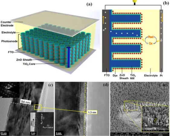
Figure 4.1: Illustrative representations of (a) a 3D schematic of the TiO2–ZnO
core–sheath composite structure and (b) the related electronic dynamics of electron transfer in the DSSC. (c) TEM and HRTEM images of ZnO (10 ALD cycles)-coated TiO2 NWs; the SAED pattern and HRTEM images in the inset
prove the growth of a single crystalline rutile phase. (d) HRTEM image estimating the thickness of a ZnO sheath layer to be 1.3 nm for 10 ALD cycles. (e) SEM images (cross sectional) of densely-packed TiO2 NW arrays.
... 30
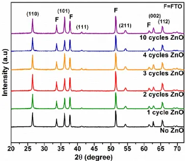
Figure 4.2: XRD patterns of TiO2–ZnO core–sheath composite structures for
xiv
with a standard diffraction pattern of rutile structure of TiO2 with the prominent peak for (110) direction. ... 31
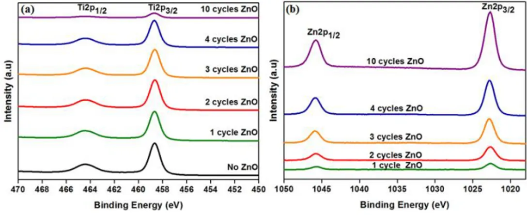
Figure 4.3: XPS spectra of a) Ti2p and b) Zn2p for TiO2-ZnO core-shell .... 32
Figure 4.4: Core-level XPS spectra of O1s from different ALD cycles coated
TiO2 deconvoluted to three different peaks indicating the presence of three
types of oxygen, lattice oxygen (LO), oxygen vacancy (VO) and chemisorbed
oxygen (CO) ... 33
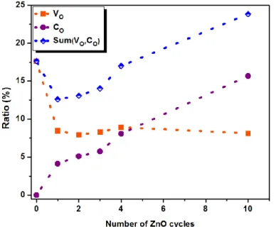
Figure 4.5: the ratio of the areas associated with VO and CO peaks to total area
of O1s in which the concentration of VO defect states stays almost constant
after one cycle deposition of ZnO while CO follows an upward trend... 33
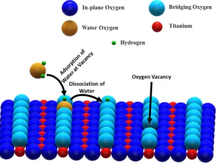
Figure 4.6: Depiction of the mechanisms associated with water adsorption
and dissociation. ... 34
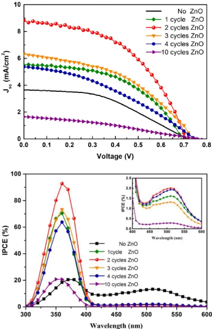
Figure 4.7: PV parameters dependence on the ZnO deposition cycles on TiO2
NWs in DSSC. (a) J -V curves and (b) The IPCE for the DSSCs consisting of the bare TiO2 and ZnO coated TiO2 core-shell composite photoanodes. The
inset shows magnified image of the IPCE for wavelengths in the range of 400-600 nm. ... 37
Figure 4.8: Excited state electron radiative decay of N719 dye sensitizer for 0,
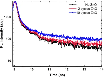
2 and 10 cycles ZnO coated TiO2 NWs for an excitation of 370 nm. ... 38
Figure 4.9: The PL spectra for different ZnO cycles coated TiO2 NWs
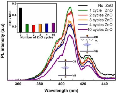
samples for an excitation wavelength of 320 nm. All samples show a near band-edge emission (NBE) at 408 nm arising from e-h recombination across the conduction band (CB) and valance band (VB) of TiO2 and a shallow
surface defect traps emission (STE) centered at 424 nm. The inset shows the ratio of STE / NBE. ... 39
Figure 4.10: Electron recombination rates for different DSSC devices
xv
ALD ZnO cycles obtained from transient photovoltage decay measurements. ... 41
Figure 4.11: The amounts of dye adsorbed on the surface of TiO2 NWs
coated with different numbers of ALD ZnO cycles, showing a sharp increase for the sample coated with two cycles. For additional cycles,the adsorbed amount follows a gradual increase. ... 43
Figure 4.12: UV–Vis absorption spectrum of N719 sensitizer dye and max
absorption is observed at 378 nm and 514 nm. ... 43
Figure 4.13: Concentration versus absorbance graph of N719 at 514 nm. The
calibration curve of dye obtained from 5 different dye concentration (75, 62.5, 50, 25, 10, and 5 μM in 1 mL) and each sample immersed in 1mL of 1:1 ethanol–0.1 M NaOH solution for desorption of the dye. ... 44
Figure 4.14: CLs of a) Zn 2p3/2 and b)Ti 2p3/2 recorded on TiO2 –ZnO
heterojunction. All peaks have been fitted to Voigt line shapes using a Shirley background, and the VB values are determined by linear extrapolation of the leading edge to the baseline. ... 45
Figure 4.15: CLs and VB Spectra of Zn 2p3/2 and Ti 2p3/2 recorded on pure
ZnO and TiO2 samples (VBM values are determined by extrapolating of
leading edge to the base line.) ... 45
Figure 4.16: 7 (αhν)1/2 versus hν plot for the bare rutile TiO2 structure ... 46
Figure 4.17: Energy band diagram of a DSSC showing band alignment in the
TiO2–ZnO interface. Some photoexcited electrons will be captured by the ZnO
well, while the rest will be injected to the CB of TiO2. The ZnO passivation
layer will reduce recombination rates by reducing surface trap states at the interface and inducing surface band bending at the TiO2 surface. ... 47
Figure 5.1: (a) Schematic of the DSSC design consists of MLAR ORMOSIL
coating (three-layer anti-reflective (AR) coating) single side coated TCO glass substrate, titania paste as photoanode, dye as photosensitizer, electrolyte as
xvi
electron transfer mediator, Pt-coated conducting glass as counter electrode. This AR coating which is a superhydrophobic porous film can provide self-cleaning property of the cell, blue spheres and brown particles on the surface represent the water droplets and dirt molecules, respectively. (b) The schematic illustration of AR coating with three-layer and its effect on light reflection reduction through gradual increasing of the refractive indices as 1.1, 1.2, 1.4, respectively to match it to the bare glass refractive index (1.5). (c) Top view SEM images of three-layer porous thin film. The inset shows the water contact angle of the surface which is 156° indicating superhydrophobic property of the porous film. (d) Higher magnification SEM image of the surface. ... 54
Figure 5.2: Transmission spectra of uncoated glass, ORMOSIL coated glass
and glass after bladed of AR coating ... 55
Figure 5.3: (a) Variations of UV-Vis optical transmittance spectra for the
ORMOSIL coated (blue) and uncoated (red) samples. For the whole range, 300nm-800nm, the amount of transmittance has increased and an average increase of 6.5% is recorded for visible spectrum. (b, c, d) One-to-one comparison of JSC-V characteristics of the ORMOSIL coated cells under different incident angles of incoming wave (0°, 15°, 30°). The ORMOSIL coating has been removed by razor blade and acetone and used as the uncoated sample. It is shown that the amount of JSC has increased by 23%, 32.1% and 84.6 % for different incident angles of 0°, 15°and 30°, respectively. ... 57
Figure 5.4: IPCE curves are collected in a wavelength range of 250nm-600nm
for the both ORMOSIL coated and uncoated cells. The amplitude of maximums located at 370nm and 520nm are improved by about 19% and 11%, respectively. The three-layer coating significantly improves IPCE efficiency for the solar cell. ... 58
xvii
Figure 6.2: SEM images of 3D TiO2 nanonetworks a-c) before and d-f) after
calcination (bar scale: 1 µm) ... 64
Figure 6.3: TEM images of 3D TiO2 nanonetworks a-c) before and d-f) after
calcination. (bar scale: 50 nm) ... 64
Figure 6.4: Raman of 3D TiO2 nanonetworks for different ALD cycles ... 65
Figure 6.5: versus plot for TiO2 templated structures with different
ALD cycles and corresponding band gaps of 3.39, 3.33, 3.24, respectively. .. 66
Figure 6.6: DSSC devices with 100,150 and 200 cycles templated TiO2 a)
xviii
LIST OF TABLES
Table 2.1: Analogy of subsystems between photosynthesis and DSSC ... 7
Table 4.1: Atomic concentrations extracted from XPS survey scans ... 32
Table 4.2: J–V parameters for the experimental devices with different ZnO
ALD cycles under AM 1.5 G filtered spectral illumination at an incident intensity of 100 mW/cm2. ... 36
Table 4.3: Results obtained from XPS valence band spectra ... 47
Table 5.1: Photovoltaic parameters for the ORMOSIL coated photoanode in
DSSC with different incident angles under AM 1.5 G filtered spectral illumination at an incident intensity of 100 mW/cm2. ... 56
Table 6.1: J–V parameters for the experimental devices of 3D TiO2 Networks
1
Chapter 1 Introduction
Since the industrial revolution, starting from several decades ago, energy concern is the most vital issue for today’s modern society. On the other side, population explosion continues and consequently demands for energy supplies are skyrocketing. This unavoidable gap between the limited energy resources and ever-increasing demand will be more pronounced moving toward halfway through this century. The upcoming energy crisis does not only have an effect on economic and political status of the society but also it will be closely attributed to health and environmental issues. How and to what extent each country will be influenced is debatable. It can be said that the energy use is directly proportional to living standards determined by a worldwide factor called the human development index (HDI). HDI is an analogical measure of progress—a composite index of life expectancy, years of schooling and income [1]. What we can understand from HDI is that as more electricity is used, higher HDI increases and better standard of living is obtained.
Since the investment of fossil fuels, the human’s main source of energy was provided by this resource. According to U.S Energy Information Administration (EIA) [2], the contribution of different energy resources consist of oil (37%), natural gas (28%), coal (18%), nuclear (8%), and renewable energy (9%) such as biomass (4.4%), hydro (2.8%), wind (1.5%), geothermal (0.2%) and solar (about 0.4%). It is expected that traditional sources will continue its major contribution to world’s energy mix till the end of 2020 with an ongoing decline out to 2050. Therefore, now more than ever before, several ongoing interests have motivated the societies around the globe to harvest alternative and renewable energy sources such as solar cell, fuel cell, wind power, geothermal energy, biomass, hydroelectric and so on. Renewables are expected to grow rapidly and supply just fewer than 13 percent of the energy needs by 2040 with EIA forecasts. Since there is a tremendous capacity in solar energy due to the expected energy generation capacity of 23000TWy/year, solar energy regarded as one of the most reliable, abundant, clean energy sources among different renewable energy sources,
2
and it allows energy generation in remote areas. That’s why we need to use solar in an efficient way to produce electricity. Photovoltaic (PV) systems convert the energy of the light coming from the sun (photons) into electricity and they are commonly known as “solar cells”. This process is coined as the photovoltaic effect. This effect was discovered first by Becquerel in the late 1830s. In 1905, A. Einstein won the Nobel Prize with the explanation of photoelectric effect. There was a big breakthrough in 1954 because the first crystalline silicon solar cell was invented in Bell Telephone Laboratories (4%). After 4 years, it was used on an electrical power for a space satellite called Vanguard I and launched in 1958.
Following the world energy crisis in the mid-1970s, companies realized that crystalline Si solar cells would be so expensive in the future, so great efforts and millions of dollars were spent to build cheaper and more efficient solar cells for residential and commercial uses. In 1976, David Carlson and Christopher Wronski fabricated the first amorphous Si photovoltaic cell consisting of the major portion of the present world PV market including power rural health clinics, refrigeration, water pumping, telecommunications, off-grid households and modern flat panel displays. Amorphous form of silicon (a-Si) is considerably cheaper material than its crystalline form used in traditional solar cells.
In the 1980’s, the solar PV became a popular power source for consumer electronic devices, including calculators, watches, radios, lanterns and other small battery-charging applications [3]. There was a steady progress towards higher efficiency solar cells and the first thin film solar cell exceeded 10% efficiency using copper sulfide/cadmium sulfide at the University of Delaware.
Starting with 90’s, there were large scale production of GaAs, other III-Vs, CuInSe2 and CdTe based multi-junction solar cells with more than 15%
efficiency. Despite the revolutions in utilizing new semiconductors for achieving high efficiency solar cells, a new path was discovered for photovoltaic community through the use of organic semiconductors. At first, it
3
was found that soluble fullerene derivatives (as acceptors or n-type semiconductors) connected to soluble p-type semiconductors (donors) can make a layered structure which will efficiently convert the light into the electricity. This generation of solar cells can easily be made through a simple coating technique. After emergence of this type of solar cells, nanostructured inorganic-organic hybrid solar cells (Dye sensitized solar cell and organic solar cells) were proposed as a promising approach to further lower production costs and provide efficient solar energy conversion. Since the invention of DSSC in 1991 by Micheal Grätzel and Brian O’Regan, a lot of attentions have been paid on these “state of art” PV devices. This thesis is on this type of solar cells.
1.1 Motivation of the thesis
Global energy crisis is a lingering problem that world is facing because the gap between energy supply and demand is significantly increasing day by day. In order to circumvent this problem, solar energy option amongst renewable energies can be considered as the most abundant and promising alternative energy sources.
Our motivation in this study is to make a bridge between our knowledge and current-to-future solar cell technologies. For this aim, in this thesis, we have developed photoanodes for performance enhanced dye sensitized solar cells which are the most successful approach of artificial photosynthesis. We will propose three main ideas to improve PV performance of typical DSSC designs and the contribution of each of these ideas in the device overall performance would be scrutinized.
1.2 Organization of the thesis
This thesis consists of eight chapters. The following chapters are outlined below:
4
Chapter 1 points out energy crisis and gives general information about photovoltaic cells, its historical background and current-future status.
Chapter 2 provides basic information about device structure, key components, operation principle and impact of different factors on device photovoltaic functionality. Here we review the recent trends in development of DSSC technology.
Chapter 3 gives the detailed information about the characterization methods including materials, photovoltaic performance, time-resolved transient and optical characterizations.
Chapter 4 presents our study on surface engineered angstrom thick ZnO-sheathed TiO2 nanowires as photoanode in DSSCs and gives details of
experimental methods, presents the results of fabricated device and discusses the reason behind this enhancement in the device efficiency.
Chapter 5 discusses multifunctional antireflection coatings for omnidirectional reduction in the surface reflection and provides information about the materials, experimental techniques and device preparation steps.
Chapter 6, peptide nanofiber network templated ALD-grown TiO2
nanostructures are investigated as the photoanode for DSSC. The details of the proof-of-concept devices are also presented.
Chapter 7 concludes the whole thesis providing a summary of the completed projects and explains key challenges with recommendations to solve them.
5
Chapter 2 Scientific Background
2.1 Introduction to Dye Sensitized Solar Cells (DSSCs)
Dye Sensitized Solar Cells (DSSCs), also called Gratzel cell, as a third generation solar cell technology, includes new and innovative structures compared to thin film and conventional silicon solar cell technologies. DSSC was introduced for the first time over 20 years ago by Gratzel and co‐workers who demonstrated the emulation of the light absorption and electron flow of photosynthesis by different elements to produce electricity [4].
Up to now, DSSC has reached efficiencies up to 15 % on small laboratory scale cells and sub modules of 8 % efficiencies have been reported by companies which lead this technology closer to market and commercial applications.
2.1.1 DSSC Inspired by Photosynthesis
Photosynthesis is of paramount importance for plants, single-cell organisms and also for animate beings that require oxygen. An understanding of photosynthesis is so valuable because it uses low energy starting materials triggered by harvested sunlight energy and during chemical reactions water and carbon dioxide is converted into chemical energy stored in simple sugars (glucose). Thus, the first idea of making DSSC was inspired by principles and materials of the photosynthesis process [5] which consist of complex sequence events, but simply it has two stage processes. The first stage is light-dependent reactions since solar energy is required and the second one is the dark (light-independent) reactions due to lack of need to solar energy.
Light dependent reactions:
In these reactions, sunlight triggers the movement of electrons (electrical current) to cause the chemical change on the -thylakoid membranes- innermost
6
membrane of the chloroplast. During the light-dependent reactions, chloroplasts absorb solar energy and two energy storing molecules (Adenozin trifosfat ATP as chemical energy and reducing agent, oxidized dihydro-nicotinamide-adenine-dinucleotide phosphate, NADPH as reducing agent) are produced. At the same time, water molecules are split which causes oxygen release (as a by-product) and this is an essential part of photosynthesis process.
Dark (light-independent) reactions:
During this process, energy stored in ATP and NADPH is consumed for simple sugars (such as glucose) formation from carbon dioxide taking placed in the –stroma- cytoplasm" of the chloroplast. The produced sugars such as glucose are stored as chemical energy for later energy source of usage at cellular respiration or its conversion to organic molecules (proteins, carbohydrates, fats/lipids, or cellulose and so on) by the cells. The below chemical equation simply summarizes the overall photosynthetic reaction
where, carbon dioxide and water are ultimately converted to carbohydrates and oxygen.
To have better understandings on the analogous between photosynthesis and DSSC, we can clarify the imitation in the following way:
Figure 2.1: Light conversion analogy between photosynthesis and dye sensitized
solar cell (DSSC). a) Sunlight is absorbed by chlorophyll. H2O and CO2 enter the
stomata. Chemical energy is formed by water under light and consequently carbohydrates and oxygen are the outcome of rearrangement between chemical energy and carbon dioxide (yield=0.2%). b) Sunlight is absorbed by dye molecules which work as photosensitizer to make electrical energy. The photo-excited electrons
7
are injected to the conduction band of the TiO2 and collected by the external circuit.
On the other side, holes complete the circuit by diffusion through the electrolyte mediator (yield>10%).
DSSC is a photoelectrochemical system which behaves like a molecular machine based on a photosensitive pigment and it consists of organic and inorganic materials (see Table 2.1). In the Gratzel cell light absorbing pigments such as chlorophyll are replaced by the organic dye monolayer. The water is replaced by electrolyte and split oxygen as an electron donor and oxidation product, respectively [2],[3]. Furthermore, the wide band gap nanostructured semiconductor layer (porous titanyum dioksit/titania nano-structure) is analogous to the chloroplast in leaves, in that it mimics the naturally occurring light absorbing protein called NADPH as a scaffold for the self‐ assembly of dye molecules per volume and finally carbon dioxide acts as the electron acceptor.
In natural photosynthesis, the existing NADPH inside the thylakoid membrane acts as chlorophylls and carotenes arranger in a specific and fixed orientation with respect to each other. By this way, vectorial energy transfer to the photosynthetic reaction centers can be optimized. That’s why it can be said that TiO2 has a dual role in DSSC since it acts as an electron acceptor and
charge carrier transport layer [8].
Table 2.1: Analogy of subsystems between photosynthesis and DSSC
Subsystem Photosynthesis DSSC
Electron acceptor CO2 TiO2
Electron Donor H2O/O2 Electrolyte
Photon Absorber Chlorophyll Dye
2.1.2 Advantages of DSSC
The solar cell technology can be grouped in three generations: crystalline solar cells (~350 µm film thick) as the first one [9], thin film solar cells (~1 µm film thick) including CuInGaSe2, CdTe, a-Si:H etc. as the second and
8
quantum dot solar cells [12], and recently emerged perovskite solar cells as the third generation solar cells [13].
Although silicon based solar cells have high efficiencies, but they are so expensive mainly due to the energy intensive purification and crystallization processes. In contrast, thin film solar cells cost much less and use less material but they have lower efficiencies. To come to grips with the complexity of cost and efficiency, third generation solar cells are emerged with low cost production techniques, together with relatively high efficiencies. Owing to extensive recent efforts spent on this generation, currently the prices of third generation solar cells continue to drop while their efficiencies are approaching to the limits of the silicon based photovoltaic technology. The major advantages of DSSC listed below over other first and second generation solar cells enable it to be used for various functions and cell configurations in DSSC:
The materials used in DSSC are non-toxic, environmental friendly.
Low-cost processing equipment which make DSSC vastly cheaper than that of silicon solar cells. Therefore, more surface area can be covered for an equivalent cost.
Low sensitivity to nonstandard conditions of solar incidence angle, temperature and irradiation (shadow and ambient temperature change). Even, when the temperature heats up from 20 to 60 ºC, it operates in an efficient and stable way. However, conventional Si cells exhibit a significant decline over the same temperature and reach an amount of approximately 20% of their nominal efficiency.
DSSC is a bifacial cell which provides capturing light from all angles and both sides.
It shows multi-color range possibilities achieved by changing the dye, either organic or inorganic.
The performance of DSSC is stable for a long period of time [4].
It can be flexible which this in turn provides innovative device structures.
9
2.2 Basic Structure of DSSC
The typical architecture of DSSC is constructed from negative electrode (so called working electrode or photoanode) which is sensitized with organometallic dye molecules as light absorbing layer and platinized glass cathode as a counter electrode, placed in front of photoanode with a parallel configuration (Figure 2.2). The space (~40 μm) between two isolated electrodes is commonly filled by the liquid iodide/tri-iodide redox couple due to its good stability and reversibility acting as the hole conducting media.
The mesoporous n-type wide band gap inorganic semiconductor layer plays a key role as photoanode in the device. In the conventional DSSC, titanium dioxide (TiO2) layer (~10µm) has interconnected architecture with anatase
phase and diameter of ~10‐20 nm deposited on optically transparent conductive oxide electrode (TCO, generally florine-doped tin oxide glass). Dye sensitized solar cell with high efficiency is achieved through the molecular engineering of porphyrin sensitizers. In following part, we will explain each component in detail.
Figure 2.2: Conventional DSSC structure
2.2.1 Transparent Conductive Oxide Substrate
Transparent conductive oxide (TCO) substrates have been heavily used in various types of solar cells and other optoelectronic applications owing to their unique properties. This family of conducting substrates can provide low sheet resistance together with having high transparency which makes them an excellent option for designing high efficiency solar cells such as DSSC. Particularly, low sheet resistance will increase the collection efficiency of the
10
DSSC and due to its transparency most of the light will reach to the sensitized photoanode. Apart from these remarkable optical properties, TCOs can sustain under harsh chemical environment and keep their durability through high temperature processes such as sintering.
In general, there are different types of metal oxide transparent conducting substrates. The most typically used compounds are; fluorine doped tin oxide (FTO), indium doped tin oxide (ITO), aluminum doped zinc oxide (AZO) and gallium doped zinc oxide (GZO) [14]. Among all of these compounds, FTO and ITO are the most popular options for device applications. Industry standard ITO can provide a sheet resistance as low as 5Ωsq-1 and a transparency of 90% over the visible spectrum. However, indium is not earth abundant and due to its limitations such as mechanical fragility, non-compatibility on strong acid environment and having high sheet resistance at high temperatures, FTO is highly preferred for DSSC application [15]. Currently, most of the DSSCs are constructed using FTO glass substrates with 8-15 Ω/sq resistance and 80% transmittance at 550 nm. FTO coating on glass substrates is performed generally by physical vapor deposition systems and other deposition systems like spray pyrolysis.
2.2.2 Semiconductor Photoanode
Wide band gap metal oxide semiconductors are generally preferred for the photoelectrode layer in DSSCs. The band gap of these semiconductors is typically larger than 3eV to provide high transparency of the photoanode over the whole UV-Vis-NIR spectrum. Several morphologies can be utilized to make this semiconducting layer including, colloidal nanoparticles (NPs) [16], nanowires [16],[17] (NWs), nanotubes [19] (NTs) and other highly branched three dimensional structures [20]–[22]. The most widely used design architecture consists of TiO2 colloidal NPs paste. This morphology can ensure
an effective surface area for dye adsorption desired for high performance DSSCs. However, the discontinuities among NPs will impose an unavoidable increase in the recombination between the photogenerated carriers and electrolyte species which consequently reduced the collection capability of the
11
cell. However, NWs and NTs will introduce a continuous 1D structure in which the probability of electron recombination will considerably reduce compared to that of NP based DSSCs, but they would offer much less surface area. In addition to these various types of designs, the choice of the metal oxide semiconductor layer is another factor which can be used to optimize the device efficiency [23],[24]. Chemical stability, high electron mobility and high adhesion to TCO are the most important requirements for this layer. SnO2
[25], ZnO [26],[27], Nb2O5 [28],[29], ZrO2 [30],[31] and TiO2 are the
potential metal oxides which are examined in DSSC structures. Although, TiO2 is the mainly utilized semiconductor for DSSC due to its high stability,
high photocatalytic activity, ZnO with mobility much higher than that of TiO2
is one of the favored options to replace TiO2 based cells. However, it was
demonstrated that ZnO was never replaced with TiO2 for high efficiency
DSSC application due to its low photo electrochemical activity [26], [27].
Up to now, the highest efficiency of the DSSC was attained by using TiO2.
Taking all of these factors into consideration, it is clear that different factors related to semiconductor photoanode are one of the key factors on the cell efficiency. Type of the semiconductor layer, design architecture and substantial treatments can be conducted to improve device efficiency.
2.2.3 Dye Sensitizer
Sensitizer is the major component of the DSSC which acts as absorbing active layer of the cell. Primarily, it absorbs incoming photons over wide range of solar spectrum from UV to near IR region. This photon will generate the electron and hole pairs via excitation of an electron from HOMO (highest occupied molecular orbital) to LUMO (lowest unoccupied molecular orbital) of the dye. Afterwards, this electron will be injected to the conduction band of the photoanode and it will be collected through this layer and hole will be conducted by the electrolyte toward the counter electrode layer.
Dye has a function to absorb light and create electron and hole pairs. Therefore, the absorption capability of the dye through the solar spectrum is
12
one of the main factors for attaining high efficiencies. In recent years, different types of dyes were prepared with the main goal of 1) increasing the extinction coefficient of the dye and 2) extension of the dye absorption tail toward visible and NIR region 3) good adsorption (chemisorption) to semiconductor layer depending on the molecular structure 4) high injection yield of excited electrons into semiconductor layer with a faster response compared to its relaxation to ground state (valence band), 5) having stable oxidized form allowing it to be regenerated by an electrolyte and 6) stable long life time (108 cycle turnover, nearly 20 years). In total, there are three classes of photosensitizers: metal complex sensitizers [32], metal-free organic sensitizers [33], and natural sensitizers [34]. However, transition metals based photosensitizers have been demonstrated to be the most suitable option so far. Especially, polypyridyl complex of ruthenium with one or more carboxylic acid groups becomes the main product and they are used to develop other dyes. Generally, the carboxyl groups on the dye will assist an effective adsorption of the dye to the mesoporous photoanode. Moreover, a considerable increase in the efficiency of DSSC can be achieved with utilization of metal to ligand charge transfer (MLCT) which is the case for N3 dye. MLCT modifies the electron position from Ru to the p* orbital and consequently increases the electron injection capability of the dye to the conduction band of TiO2. It should be noted that in MLCT, HOMO level of
dye molecules are positioned near to metal particles and oppositely LUMO level of the dye molecules are positioned near ligands. Furthermore, N719 dye was obtained through engineering of the N3 bond structure. N719 shifts the conduction band of TiO2 positively and increases the open circuit voltage of
the cell. Although these dyes are able to provide nominal efficiencies for the DSSC but both of them can absorb the light efficiently below the 600nm. Therefore, a new dye was invented; N749 or black dye which was able to extend the light absorption to longer wavelengths and consequently more current density is produced. On the other end of the scale, Z907 was another dye studied to solve the stability problem of the above dyes at temperature of nearly 80 ºC. Z907 dye does not show any degradation for 1000 hours at 80
13
ºC. As it can be clearly seen, all of the studies performed in this area are aiming to tackle with a specific deficiency of the dye such as light absorption and thermal stability.
2.2.4 Electrolyte
Another component of the DSSC is the electrolyte. Electrolyte is a liquid based charge transport layer; its main function is to regenerate the dye after injection of an electron to the photoanode. Also, this layer is hole transport layer to transfer positive charges to the counter electrode layer. The long-term stability of DSSCs is defined by electrolyte [35]. Thus, to obtain a proper working electrode following requirements should be met: (1) fast electron diffusion with the help of low viscosity, small redox species and high electrical conductivity (2) high efficient interfaces of electrolyte/semiconductor and electrolyte/counter electrode (3) low imposing degradation of dye or desorption of the dye from the photoanode surface (4) low absorbing light in the visible region.
At the end of this section, it should be noted that there were a lot of studies on the development of new electrolytes to get long-term stability. Electrolytes for DSSCs can be categorized into three types: liquid electrolytes [36], solid state electrolytes [37], and quasi solid state electrolytes [38]. The most frequently used one is liquid electrolytes (organic and ionic electrolytes) with a redox couple.
2.2.5 Counter Electrode
The counter electrode (cathode) is used for the reduction of the oxidized species of electrolyte. For proper operation, the counter electrode should have good catalytic activity. The redox species reduction in cathode is faster than anode. To date, the most preferred catalyst is platinum which maintains the reduction reaction fast as well as high transparency, but its performance mainly depends on deposition techniques on TCO substrate such as thermal decomposition of hexachloroplatinic salt in isopropanol, electro deposition,
14
sputtering, vapor deposition, and screen printing. Here, the main point which should be considered related to Pt catalyst is its performance reduction in time and catalytic activity is deteriorated due to its removal off of the substrate (etching) in the presence of electrolyte. In addition, it is an expensive metal and its preparation requires high temperature fabrication methods (400ºC), thus graphene [39], activated carbon [40], conductive polymers [41] have been investigated as alternative materials for cathode; however, their electrical efficiencies were not as high as Pt catalyst.
2.3 Electron Transfer Dynamics of DSSCs
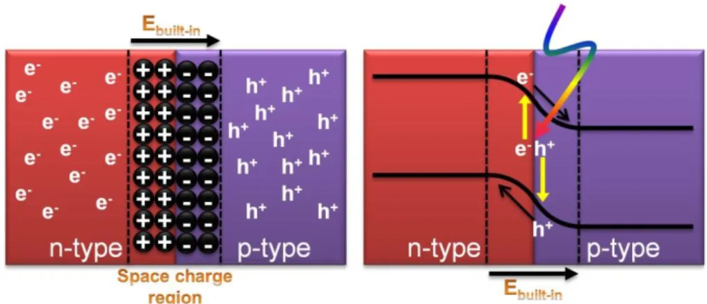
It should be noted that photovoltaic processes in DSSC such as charge separation is different from conventional p-n junction based solar cells. In p-n junction the separation is assisted by built-in electric field across the interface. However, this process is originated from kinetic competition of the excited electrons at the organic/inorganic interface in DSSC.
Solar energy is converted to electrical energy by means of several kinetic-based processes involved inside the solar cell. As shown in Figure 2.3, in the case of conventional p-n junction solar cells, the kinetic is different from the DSSC. When an n-type material comes to the contact with a p-type material, the depletion region will be created at the interface of the p-n junction. As the consequence of this depletion region, a built-in potential will be made in which this potential separates electron and hole pairs. Afterward, electrons will transport via n-type semiconductor and holes will diffuse inside the p-type layer. Considering all of these explanations, all processes including light absorption, charge separation and charge collection are occurred at semiconductors in which these semiconductors can be same or different. However, due to the small dimensions of the photoanode particles in the DSSC, the possibility of depletion region formation is negligible and it works based on kinetic competition of the carriers at organic/inorganic interface. DSSC is a photo electrochemical device in which all of the injection,
15
collection and absorption processes occur at different materials. As the result of these dynamic processes photocurrent and photovoltage are produced.
Figure 2.3: a) Energy band diagram of conventional p-n junction under short circuit
conditions; b) Charge separation under illumination
This photovoltage is equal to differences between the Fermi level of the semiconducting photoanode and the electrolyte redox potential. A number of processes (photoexcitation, electron injection, electron collection, dye regeneration, recombination) that occur inside the cell during its operation can be illustrated in Figure 2.4 and following related reactions are summarized.
Figure 2.4: Processes involved in sunlight conversion to the electricity inside a
16 ( ) ( ) ( ) ( ) ( ) ( ) Cell: ( ) 1. Photoexcitation
When a photon with energy higher than the band gap of the dye comes to the ground state (S) of the dye molecules adsorbed on the photoanode, it generates the electron and hole pairs. During this process, the electron will be excited to the excited state (S*) and hole will stay at the ground state (S). Some portion of these excited carriers will come back to their unexcited state through a relaxation process which is typically a ~ few femtosecond process [42] [43].
2. Electron Injection
After photoexcitation of the dye and before relaxation across the dye band gap, some of the electrons on the excited state will be injected to the conduction band of the semiconductor photoanode layer. Obviously, to have this process possible, the conduction band of semiconductor layer should be at lower energies than the excited state of the dye. The injected dye electrons will be positioned to the conduction band minimum of the photoanode layer via a process called thermalization. Another driving force comes from the entropy differences between the dye and photoanode. Electrons are tending to move in the direction of photoanode due to large number of delocalized states compared to dye molecules. Final mechanism is created by the anchor carboxyl group of dye molecules. To supply the adsorption of dye to
17
photoanode, a photon is donated from anchor group to photoanode. Therefore, the photoanode surface is more positive and dye surface more negative which help to separate charges and reduce recombination [44]. While both photoexcitation and electron injection take place at few femtosecond (fs) and sub-picosecond (sub-ps) scales, respectively, electron relaxation from excited state to ground state occurs at a nanosecond (ns) range [43]. Therefore, it is relatively much slower than injection time and ensures a high injection yield. On the other side, dye will lose one electron and it becomes an oxidized product. So the dye (S*) becomes (S+).
3. Electron Collection
The injected electrons will come to the conduction band of the semiconductor and will be collected by FTO layer. During the collection process, these electrons diffuse inside the TiO2 conduction band and experience several
trapping/de-trapping processes before reaching to the collector. The existence of surface or bulk trap states and the contact between the electrolyte and TiO2
layer can reduce device efficiency considerably by a process called recombination. It is possible for the electrons to recombine with the holes in the dye valance band or electrolyte species (it has been found that the second one is dominant). On the other hand, the existence of the surface and bulk defect states can reduce the collection capability of the device via trapping the electrons. The capability of the electron is mainly depended on the morphology, crystallinity and the mobility of the semiconductor.
4. Dye regeneration
As explained above, when a dye molecule gives an electron to the semiconductor, it turns to an oxidized product. Therefore, there would be a mechanism to regenerate the dye. This occurs with the help of the electrolyte. An electron will pass from the counter electrode (Pt) to the electrolyte to provide the reduction reaction. In other words, the electron is transferred to the electrolyte where it reduces the oxidant species, Ox. Subsequently, the
18
reducing agent formed, Red, oxidizes the excited dye, S+, and returns it to the inactive/ground state, S.
As an instance, for the most typically used I3-/I- (triiodide / iodide) redox couple, I3- reduced to iodide ion I- and subsequently, electrontransfers back to the dye molecule. Afterwards, iodide ion reforms to triiodide and dye molecule will return to inactive state (S). Here, I3- and I- is called as an oxidizing molecule and reducing molecule, respectively. This regeneration process takes place in a μs time scale [42],[43].
5. Recombination
The main detrimental process responsible for device performance is charge recombination. Recombination of the injected electrons is one of most restricting factors which reduce device efficiency considerably. The recombination of the carriers is an unwanted process in which electrons are captured with other species before getting collected at the TCO. This process is mainly between two routes; the reaction between 1) the injected electrons and dye holes and 2) the injected electrons and redox species. Although both mechanisms are responsible for device efficiency reduction but the portion of second process is supposed to be dominant. This recombination, -also called back reaction of the electrons, is a millisecond (ms) scale phenomenon. Therefore, compared to injection response time (which is at the order of 100 ps) its response is quite slow and a big portion of the electrons can be collected by TCO. However, this process has still undeniable detrimental effect on device performance and its impact should be mitigated. In recent years, several studies have been performed to retard electron back reaction and reduce the recombination rate of the carriers. Together with all of these mechanisms, a part of this recombination can occur through trap states in which this localized energy states trap the electrons and pass it to redox species. Considering all of these facts, a low recombination rate can be achieved with proper design structure in that electron back reaction is delayed and surface trap states are passivated.
19
Chapter 3 Characterization Methods
The experiments and characterizations are conducted in the UNAM Cleanroom Facilities (UCF) (class 100 and 1000), Okyay Group Laboratories and other characterization laboratories in UNAM at Bilkent University.
3.1 Material Characterization
Non-destructive analysis technique of X-ray diffraction (XRD) has been utilized to investigate the crystalline phase and morphology of the photoanodes. This has been carried out by X-ray diffractometer (XRD, model Panalytical X’pert Multi-Purpose) and patterns have been collected in the range of 2𝜃 using Bragg–Brentano geometry (Cu K𝞪). Scanning electron microscope (SEM, FEI – Quanta 200 FEG, operated at 10 kV) and transmission electron microscope (TEM, Tecnai G2-F30, FEI, operated at 200 kV) have been employed to characterize the morphology and dimensions of the structure. TEM samples are prepared on a holey carbon coated copper grid. Selected area electron diffraction (SAED) analysis is also utilized to identify the growth direction and crystallinity of the nanowires. Investigations on constituent elements at the surface of the samples have been done using X-ray photoelectron spectroscopy (XPS, Thermoscientic K-Alpha, Al K-Alpha radiation, hʋ=1486.6 eV). Moreover explorations on 1) the band alignments at the core shell interface, 2) elemental analysis and presence of surface defects, have been assisted by XPS performed at survey mode by operating flood gun to prevent charging surfaces. In addition to this, a contact angle meter (OCA 30, Dataphysics) is used to obtain static contact angles of coated samples by using 4µl dispersed water droplet onto the surface.
3.2 Photovoltaic Performance Characterization
The photovoltaic cells have been characterized with home-made current-voltage (I-V) measurement setup and incident photon-to-current conversion efficiency (IPCE) setup.
20
3.2.1 Current-Voltage (I-V) Measurement
Current-voltage (I-V) or current density-voltage (J-V) characteristic is a standard analysis technique to measure the photovoltaic performance of the solar cell. This measurement was carried out using a Keithley 2400 source-meter which is integrated with a AM 1.5 G Newport 67005 solar simulator under a 100 mW/cm2 solar light irradiation.
“AM” is the abbreviation for air mass, so AM 1.5 implies that the light has to travel 1.5 times farther than direct incidence would before reaching ground level. The power of the incident light, Pin, can be adjusted by the distance between the light source and the device, and it is calibrated at a fix amount.
Upon applying light with a well-defined spectrum and intensity (A.M 1.5G solar simulation) to a solar cell and measuring its I-V response, several solar parameters can be deduced as demonstrated in the Figure 3.1 and equations. The important parameters are open circuit voltage (VOC), short circuit current density (JSC)and fill factor (FF) and efficiency (𝞰) which can be used to compare with different devices. The maximum power, Pmax,, of the solar cell is obtained from multiplication of IMP and VMP. The open circuit voltage (VOC) is the potential difference for the case that the net current flow is zero (when I = 0, resistance → ∞). The short circuit current (ISC) is the max current flow at the cell under zero voltage bias (when V = 0, resistance → 0). Often short current density (Jsc) is preferred which defines the ratio of photogenerated current to electrode active area. Fill factor (FF) is the ratio of the maximum power (Pmax) of the device to the theoretical maximum power (product of VOC and ISC) which defines the measure of squareness of the I-V curve. Higher resistance and more recombination in a solar cell reduce the FF. The power conversion efficiency, η, of a solar cell is defined as the ratio of
Pmax to Pin per area. It is the ratio of output energy to the input energy.
21
Figure 3.1: Current Density–Voltage ( J–V ) curve of a conventional DSSC under illumination
Shape of the I-V curves can deviate from a sharp square mainly due to the effect of parasitic resistances. Shunt (RSH) and series (RS) resistances are effective in solar cells and they reduce the fill factor and efficiency [15].
3.2.2 Incident photon to-current conversion efficiency (IPCE)
Incident photon-to-current conversion efficiency (IPCE) is a characterization technique which provides information about how efficiently the device converts photons as a percentage into electrons (current) at each wavelength.
For this aim, a Xenon lamp (150 W) is utilized as an illumination source of the light. Monochromatic light is achieved with a 1200 lines/mm grating and it is chopped by a mechanical chopper at a frequency of 10 Hz. The illuminated monochromatic light has been focused on the sample surface and the cell is biased using a Keithley 2400 source-meter. The voltage of gate terminal is separately biased with a Keithley 2400 voltage supply. A lock-in amplifier is employed to detect and measure the photogenerated current through the anode and cathode ports. In an ideal case, series connection of lock-in amplifier for photocurrent measurement is advised.
The outcoming optical beam has dimensions of 400 μm (width) and 1200 μm (length). To calibrate and measure the incident power density in every single frequency, a calibrated Si photodetector (Newport 918D-UV-OD3R) with a
22
1.1cm-long efficient detection range (which is much wider than the incoming spot) is used.
As explained, the monochromator that we use utilizes a 1200 lines/mm diffraction grating to selectively produce our desired single frequency light from the white incident light. But it should be mentioned that due to the reflections off the diffraction grating, polychromatic light can be made. Therefore, together with the desired wavelength (λ), the polychromatic light is also comprised including second (λ/2), third (λ/3) and larger harmonics (λ/n) of the desired wavelength [54-56]. To suppress the existence of these higher order modes, a 500 nm high-pass filter at (Newport FEL0500) is employed in all of our measurements that are beyond the 500 nm.
The monochromator was incremented through the UV and Visible spectra to generate the IPCE (λ) as defined below
( )
( ) (
)
( ) ( )
where λ is the wavelength, JSC is short-circuit current density (mAcm-2), and
Iinc is the incident power intensity (Wcm−2).
3.3 Time-resolved Transient Characterization
In all solar cells, the incoming light generates electron-hole pair carriers that have a probability to meet their conjugate carriers and recombine with each other. In general, recombination means a dissipation of the free energy provided by the photons to heat inside the cell. In solar cell device recombination reduces the efficiency of power conversion efficiency and it is a must to keep its contribution as low as possible. To scrutinize all of these kinetic processes, a proper time-resolved characterization can provide valuable information about this few micro/nano seconds processes.