Analytic thermal modeling for dc-to-midrange
modulation frequency responses of thin-film high-T
c
superconductive edge-transition bolometers
Mehdi FardmaneshThin-film superconductive edge-transition bolometers are modeled with a one-dimensional analytic thermal model with joule heating, film and substrate materials, and the physical interface effects taken into consideration. The results from the model agree well with the experimental results of samples made of large-meander-line Yba2Cu3O7⫺xfilms on crystalline SrTiO3, LaAlO3, and MgO substrates up to
100 kHz, the limits of the experimental setup. Compared with the results of the SrTiO3substrate
samples, the results from the model of the LaAlO3and the MgO substrate samples deviate slightly from
the measured values at very low modulation frequencies共below ⬃10 Hz兲. The deviation increases for higher thermal-conductive substrate materials. When the model was used, the substrate absorption and the thermal parameters of the devices could also be investigated. © 2001 Optical Society of America
OCIS codes: 230.0040, 040.3060.
1. Introduction
Responsivity versus modulation frequency and ver-sus the temperature of edge-transition superconduc-tive bolometers has previously been investigated and reported in different studies.1–7 Major effects of the
substrate– holder and the substrate–film thermal boundary resistances on the response of this kind of bolometer as well as the modulation frequency de-pendence of the response were reported in previous studies.1–7 From the previously reported
observa-tions, there have been some efforts to predict the response behavior by use of different thermal models for this type of detector.1,3,8 –11 These efforts were in
particular for the sample types used in this study. In this paper a one-dimensional thermal model and its closed-form solution are proposed for the bolomet-ric response of thin-film high-Tc superconductive
edge-transition bolometers on thick crystalline sub-strates. The proposed model is for dc-to-midrange modulation frequencies above which the limits of the
heat diffusion into the film should also be further considered. The samples considered in this paper carry large-area superconductive patterns compared with the thickness of the substrates.
For the samples with large-area superconducting film patterns compared with the substrate thickness, the thermal boundary resistance at the substrate– holder of the samples, Rsc, was found to be consider-ably higher than that of the other sources such as the film–substrate boundary resistance Rfs, the substrate material resistance Rs, and the bulk film thermal
resistance Rf.1,3,12–14 Hence the total thermal
con-ductance of the device, Rt, was close to the value of
Rsc, resulting in Rt ⬇ Rsc. This is found to be the case at the low-end modulation frequencies.3,12 In
such a configuration the response of the samples is expected to follow a basic two-lumped-element R-C model. Then R is determined mainly by the thermal boundary resistance at the substrate– holder inter-face 共i.e., R Rsc兲, and C is mainly due to the heat capacity of the substrate materials, Cs, which is much
higher than that of the film for the considered sam-ples in this paper共i.e., C ⬇ Cs ⬎⬎ Cf兲.15–19 This is
reported to be the case up to frequencies at which the thermal diffusion length L into the substrate mate-rials is more than the substrate thickness Ls when the effect of the substrate– cold-finger interface can be seen by the heat wave propagating into the sub-strate.3,12 The increase of the modulation frequency M. Fardmanesh共[email protected]兲 is with the
Electri-cal and Electronics Engineering Department, Bilkent University, Ankara 06533, Turkey.
Received 12 June 2000; revised manuscript received 21 August 2000.
0003-6935兾01兾071080-09$15.00兾0 © 2001 Optical Society of America
beyond the values at which L⬍ Lscan cause a change in the slope of the response magnitude versus mod-ulation frequency compared with that of the basic R-C model. This was found to happen at a so-called knee frequency fL, which is dependent on the substrate ma-terial and its thickness.1,3,12 Considering the thermal
diffusion length as the characteristic penetration depth of the temperature variation into the substrate, we can determine the knee frequency from3,12
fL⫽
D
Ls2
, (1)
where Lsis the substrate thickness, D⫽ Ks兾Csis the thermal diffusivity of the substrate material, and Ks
and Csare the thermal conductivity and the specific heat 共per unit volume兲 of the substrate materials, respectively.
A different regime of frequency response behavior has been identified based on the above conditions.1,3
For frequencies less than fL, the response was found
to scale as f⫺1following the response for a basic R-C model.3,12,15,16 For frequencies higher than f
L, the
response was found to scale as f⫺1兾2because of the variation of the effective penetration depth of the temperature variation into the substrate.1,3,12 The
response follows the f⫺1兾2dependence up to the fre-quencies at which the thermal resistance of the su-perconducting film–substrate boundary Rfs is
negligible compared with the frequency-dependent thermal conductance of the substrate materials Rs.
The frequency dependence of the thermal conduc-tance of the substrate Rscan be determined from the
thermal diffusion length as
Rs⫽
1
A
冑
CsKsf, (2)
where A is the effective area of the conductive path, f is the modulation frequency in hertz, and is a cor-rection factor for the above approximation of the ef-fective length of the ac heat flow.3,14 The effects of
the temperature dependence of the thermal boundary resistance at the substrate interfaces were also found to be partly responsible for the variation of the re-sponse versus temperature while still following the basic model at any stable state.14 Hence the
ther-mal parameters used in the equations should be ad-justed for each bias temperature.
There have been different efforts made for response modeling of the edge-transition superconducting bo-lometers with and without consideration of the effects of thermal boundary resistance at the substrate in-terfaces and the self-heating or joule heating in the superconducting film.1,8,10,11 Based on the above
proposed effects of the introduced parameters, suc-cessful analyses and predictions have been made of the behavior of the response versus modulation quency curves of the samples that predict the fre-quencies at which the slope of the curve changes共the knee frequency兲.1,3 However, they have not
pre-dicted and matched the responses in all the measured modulation frequency regimes when an analytic model was used. The present proposed models have predicted and matched the measured responses of the samples at low frequencies, showing different consid-erable discrepancies at midrange or higher modula-tion frequencies.1,3 To my knowledge, in all the
proposed models and solutions, only the magnitude of the response has been considered and compared with the experimental values. This is because the phase of the response was found to be a more sensitive characteristic of the response with respect to the model and the chosen or obtained thermal parame-ters of the device.14 In this paper the results
ob-tained from the derived closed-form solution of the proposed one-dimensional model are presented. The results from the model are compared with both the measured values of the magnitude and the phase of the response of the samples.
2. Samples and the Characterization Setup Configurations
The samples studied in this paper were made of 120 –550-nm-thick granular superconducting YBa2Cu3O7⫺x 共YBCO兲 films on 0.025- to 0.05-cm-thick crystalline SrTiO3, LaAlO3, and MgO
sub-strates. The films were deposited by off-axis planar magnetron sputtering at⬃720 °C and pat-terned by a standard photolithography technique 共positive photoresist兲 modified for less damage to the YBCO material.3 The patterns were made of
either a 50-m-wide and 1.9-cm-long meander line, giving a total area of 0.017 cm2, or a 120-m-wide
and 4.8-cm-long meander line, giving a total area of 0.075 cm2, as listed in Table 1. The resistance
ver-sus temperature and the critical temperature Tcof
Table 1. Dimensions and Thermal Parameters of the Samples Obtained the Proposed Thermal Modela
Sample Number Substrate Material ds 共cm兲 Cs
冉
J k cm3冊
Ks冉
W k cm冊
Rsc冉
K W cm2冊
␣ df 共nm兲 A 共cm2兲 Rfs冉
mK W cm2冊
Cf冉
J k cm2冊
dR兾dT冉
⍀ K冊
064-03a MgO 0.05 0.53 3 6.82 2 170 0.075 4.4 642 1000 064-01a SrTiO3 0.05 0.43 0.052 5.6 1.7 220 0.017 44 655 1800 061-02a LaAlO3 0.05 0.59 0.16 8.82 1 550 0.075 27.5 131 670aThe dimensions of the substrates’ area are approximately 0.5 cm⫻ 1 cm for all the samples. d
sis the thickness of the substrate, df
is the thickness of the YBCO film, and Rscis the measured substrate– cold-finger thermal boundary resistance. The factor␣ is the fitting
parameter for the one-dimensional solution obtained from the model. Rfsis the film–substrate boundary resistance, and Cfis the heat
the samples were found to change when the film was exposed to high bias currents or thermal cy-cling under vacuum, and hence the optimal bias temperature was changed.13 The transition
tem-peratures of the samples shifted to lower tempera-tures because of high bias currents under vacuum and were recovered under a few thermal cycles, reaching a stable value under low bias currents.13
Hence the presented data in this paper are obtained with relatively low bias currents under stable con-ditions and Tc. More details about the fabrication
of the samples and their dc characteristics are pre-sented elsewhere.3,13,14
The typical configuration of the studied samples is shown in Fig. 1. The contact areas for the four-probe measurement were coated with either an ⬃85-nm layer of sputtered gold or an ⬃60-nm layer of sput-tered silver. Electrical contacts to the samples were made with copper wire 共32-gauge兲 and silver epoxy dried at room temperature overnight. To character-ize the samples, the second cold stage of a Cryo-Torr 100 was used as the cold finger by a computer-controlled heater. The temperature of the cold fin-ger could be controlled by approximately⫾0.1 K from the set points. More details of the characterization setup and the instrumentation are presented else-where.14,17,20 A sample holder was designed and
made of high purity and highly conductive oxygen-free共OFE兲 copper that was etched in an inert envi-ronment gas and coated by a thin layer of gold without being exposed to the atmosphere. The con-figuration of the holder is shown in Fig. 2.
As shown in Figs. 1 and 2, there are two thermal boundary resistances at the substrate interfaces, one at the film interface and the other at the holder in-terface. There are two major bulk areas that
con-tribute to the overall heat capacity of the samples, one that is due to the superconducting film and one that is due to the substrate materials. Here the OFE copper is considered to be a heat reservoir, the temperature of which is considered uniform at the value measured by the temperature sensor. To ob-tain a better thermal contact, a very thin layer of either Apiezon-N grease or silicon vacuum grease was used to attach the samples to the holder in the model. The effect of the grease is considered to be included in the measured substrate– holder thermal boundary resistance Rsc. The dimensional
parame-ters and the dc electrical and thermal characteristics of interest for the studied samples in this paper are given in Table 1. The given thermal conductivity and the heat capacity of the LaAlO3substrate
mate-rial in Table 1 are obtained by fit of the calculated response versus frequency curve from the model to that obtained experimentally.
The phase and the magnitude of the response ver-sus modulation frequency of the samples, which are the focus of this work, were measured by a lock-in amplifier共EG&G 5406兲, the input signal of which was amplified by an ultra-low-noise preamplifier共Model 030B, Perry Amplifier兲. A light-emitting diode 共HFE4020, Honeywell兲 with a peak radiation wave-length of⬃0.85 m was used as the radiation source for the response versus modulation frequency studies in all the measurements. The diode was placed a few centimeters above the sample, providing uniform radiation on the superconducting film pattern. The response of the samples was found to be proportional to the radiation intensity up to 2.13 mW兾cm2, which
was the limit of the source and the radiation intensity for the measurements of the results presented in this paper.
3. Thermal Modeling
From the dimensions given in Table 1 and also as relatively shown in Fig. 2, the area of the supercon-ducting pattern of the samples is large with respect to the substrate thickness. Hence a one-dimensional model is considered and applied for the studied sam-ples in this paper, with all the parameters considered for per unit area. Because of the partial lateral heat diffusion of the heat wave coming from the film into the substrate共the spreading-resistance effect兲, a cor-rection factor␣ was obtained for applying to the mea-sured Rscvalues and is given in Table 1. The value of ␣ was found to increase with the increase of the thermal conductivity of the substrate material and was highest for MgO. It was also found to increase with a decrease in the superconducting pattern area with respect to the substrate thickness, as given in Table 1, and to be higher for the small pattern film on SrTiO3 compared with that of the LaAlO3substrate
sample. As given in Table 1, the thicknesses of the superconducting films of the samples were also very small compared with those of the substrate. This allowed the consideration of a lumped-film assump-tion on the top surface of the substrate in the model. When the superconducting pattern is considered a
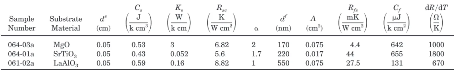
Fig. 1. Typical used superconducting thin film and the electrical contact-area patterns共metallization兲 of the samples on 1 cm ⫻ 0.5 cm area crystalline substrates.
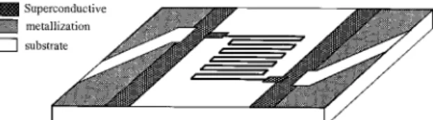
Fig. 2. Configuration of the thin superconducting film samples on a crystalline substrate in contact with the holder and the temper-ature sensor.
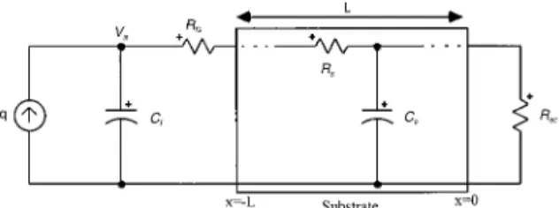
lumped film and the substrate a continuous uniform medium, the thermal equivalent circuit of the sam-ples in contact with the holder can be represented as shown in Fig. 3, where q is the absorbed radiation intensity at the surface of the sample. In this equiv-alent diagram, two thermal boundary resistances are considered at the substrate interfaces. The heat capacitance of the superconducting film is also con-sidered to be a value representing the total heat capacity of the film per unit area. The thermal conductance of the superconducting film was calcu-lated and found to be negligible compared with that of the substrate and the interfaces. For samples with thicker superconducting films, as for the screen-printed materials,17the limited heat conductivity of
the superconducting material, which is the same as that for the substrate, should also be considered. Based on the above considerations in the model as shown in Fig. 3, the derivation of the temperature variation and the corresponding thermal parameters for the samples under a constant bias current are presented in the following subsection.
A. Temperature Variation in the Substrate
To approach the complete closed-form solution to the model given in Fig. 3, first we consider the absorbed radiation power q to be applied directly to the surface of the substrate. This is ignoring the effects of the surface boundary conditions of Cf and Rfs, which
represent the effect of the thermal parameters of the superconducting film at this stage. This particular assumption and the solution to it would be the case for low modulation frequencies. At low modulation frequencies, Cfis much smaller than the contributing
heat capacity of the substrate, which can be deter-mined from Eq.共1兲.3 Also, the film–substrate
ther-mal boundary resistance Rfs, is much smaller than
that of the substrate– holder or the low-frequency
thermal resistance of the substrate Rs, determined from Eq.共2兲.
Based on the above assumptions and the steady-state solution to a general one-dimensional heat propagation equation, the temperature variation at the surface of the substrate,⌬T, is obtained. With-out consideration of the effect of the superconducting film共i.e., Cfand Rfs兲, ⌬T is obtained as follows:
⌬T ⫽ qexp共␥L兲 ⫹ ⌫ exp共⫺␥L兲 exp共␥L兲 ⫺ ⌫ exp共⫺␥L兲
冉
1 jcsks冊
1兾2 , (3)where ␥ is the characteristic thermal impedance of the substrate material defined as
␥ ⫽1⫹ j 共2兲1兾2
冉
cs ks冊
1兾2 , (4) ⌫ ⫽ Rsc⫺冉
1 jcsks冊
1兾2 Rsc⫹冉
1 jcsks冊
1兾2, (5)where is the angular modulation frequency and ks
and csare the heat conductivity and the heat capacity
of the substrate materials, respectively. The value of Rsccan be found from
Rsc⫽
1
G共W兾K兲兾A, (6)
where G is in units of watts per degrees kelvin and is the total thermal conductance of the device at dc or low-end modulation frequencies G共0兲, and A is the film pattern area. This is based on the assumption that
Gfs⬎⬎ Gs⬎⬎ Gsc, where Gfs⫽ 1兾Rfs, Gsis the total heat
conductance of the substrate, and Gsc⫽ 1兾Rsc. This
assumption has been verified for samples with dimen-sions close to those of our samples, which is discussed in detail and presented elsewhere.1,3,12,14,21,22
B. Temperature Variation at the Film
To find the voltage response to the modulated radia-tion intensities, the temperature variaradia-tion in the su-perconductive film of the samples was obtained for all considered frequency ranges. This temperature variation corresponds to the temperature change across Cfin the equivalent circuit of Fig. 3. Hence
the only temperature gradient from the top of the superconducting film into the substrate would be that across the film–substrate interface Rfs. When the
one-dimensional thermal differential equation is solved with complete boundary conditions, as shown in Fig. 3共i.e., with consideration of Cfand Rfs兲,
Fig. 3. Equivalent thermophysical diagram of the samples in
contact with the cryogenic holder, where q is the input radiation power, Cfis the lumped heat capacitance of the film, Csand Rsare the heat capacity and the thermal conductivity of the substrate material, respectively, Rfsand Rscare the thermal boundary re-sistance values at the film–substrate and the substrate– holder interfaces, respectively, and Vais the temperature of the film.
⌬T ⫽ q
冤
exp共␥L兲 ⫹ ⌫ exp共⫺␥L兲 exp共␥L兲 ⫺ ⌫ exp共⫺␥L兲冉
1 jcsks冊
1兾2 ⫹ Rfs exp共␥L兲 ⫹ ⌫ exp共⫺␥L兲 exp共␥L兲 ⫺ ⌫ exp共⫺␥L兲冉
j csks冊
1兾2 Cf⫹ 1 ⫹ jCfRfs冥
, (7)the temperature variation caused by the radiation absorption in the film is found as follows:
where q is the absorbed radiation power in the film per unit area, and Cf and Rfs are the total heat
ca-pacity of the superconducting film and the thermal boundary resistance at the film–substrate interface per unit area, respectively.
The obtained solution of Eq.共7兲 is up to frequencies at which the thermal diffusion length into the super-conducting film共for YBCO material兲 becomes smaller or comparable with the thickness of the film. This occurs while the penetration depth or the absorption coefficient length in the superconducting film is still considered to be much smaller than the film thick-ness. This frequency regime for the samples of Ta-ble 1 with a maximum film thickness of⬃550 nm is found to be much higher than that investigated in this study. As given in Eq. 共7兲, at low frequencies the denominator will approach 1 and Rfswill become negligible compared with the first term of the numer-ator, leading to the results of the one boundary con-dition problem, as given in Eq.共3兲. This is because at low modulation frequencies共below ⬃10 Hz in these samples兲 the temperature variation 共heat wave兲 reaches the bottom of the substrate and hence the heat capacity of the film with respect to that of the whole substrate material under the pattern, and also the thermal boundary resistance at the film– substrate with respect to Rs and Rscbecomes negli-gible.3,12
C. Voltage Response and Bias Current Dependence
Considering a uniform temperature variation in the film, caused by the absorbed radiation ⌬T, we can obtain the voltage response in a dc bias configuration from
dV⫽ Ib⌬T
dR
dT, (8)
where Ibis the dc bias current, dR兾dT is the slope of the R versus T curve at the bias temperature as given in Table 1, and⌬T is the temperature variation in the superconducting film as given in Eq.共7兲. Equation 共8兲 is valid within the temperature variation range within which dR兾dT can be considered constant. The maximum temperature variations of the films caused by the radiation were typically below approx-imately a few millidegrees kelvin, as measured dur-ing the characterizations presented in this paper. The transition widths of the samples were typically a few degrees kelvin, and hence the variation of dR兾dT or the nonlinearity of Eq.共8兲 was found to be negli-gible in the measured and the calculated responses. However, this would not be the case for devices ex-posed to high radiation intensities that are normally voltage biased for further stability.23,24 The effect of
the bias configuration on the response and the feed-back effect of the joule heating for each case of the voltage-biased and current-biased configurations are discussed and presented elsewhere.13
There is also a consecutive temperature variation
that is due to ac joule heating in the film caused by the resistance variation in the superconducting film that is due to the input radiation power. This effect on the response is in the form of positive feedback in the used current-biased configuration as used for the samples in this work. This ac joule heating in a first-order approximation can be considered either as a dependent radiation共or heating兲 source in parallel to the external radiation source q, as shown in Fig. 3,25 or simply as an additional term in the overall
responsivity of the sample as given in the following form3,12
rv⫺t⫽
rv
共1 ⫺ Irv兾兲
, (9)
where rv⫺tis the overall responsivity in volts per watt
and is the absorption coefficient in the film. When the effect of the absorption coefficient in the q factor in Eq. 共7兲 is considered, rvwill be proportionally re-lated to the dV given in Eq.共8兲. The effect of ac joule heating in the response of the samples studied in this study is found to be negligible for the used biased currents.
4. Measured Frequency Response and the Results from the Model
The results from the model were compared with the experimental values for the samples given in Table 1. The frequency response behavior of the samples was found to be strongly dependent on the film and the substrate dimensions as well as on the thermal pa-rameters, whereas the observed dependencies were in good agreement with the thermal model. To cal-culate the response by use of Eq.共7兲, the dc thermal parameters of Rfs, Rsc, Cf, Cs, and Ksof the samples were determined. The measured values of the above parameters are given in Table 1. The values of Rsc,
which are much higher than Rsand Rfs, were mea-sured by the method of the resistive or the dc joule heating in the film close to the transition tempera-ture Tc.14 –16,18 In this method a high bias current is
passed through the film and we measure the temper-ature rise that is due to the joule heating by measur-ing the resistance of the film. Then, knowing the temperature rise and the joule heating power, we obtain the values of Rsc. Parameters such as the film–substrate thermal boundary resistance and the thermal parameters of the substrate or the heat ca-pacity of the samples could also be obtained and ver-ified by use of the fit of the results from the model to the measured values. The values in Table 1 are given per unit area as used in the one-dimensional solution of the model.
The results from the model were investigated for thin-film samples on crystalline SrTiO3, LaAlO3, and
MgO substrate materials. The measured and the calculated magnitude and phase of the response of the meander-line-patterned YBCO films on the 0.05-cm-thick SrTiO3, LaAlO3, and MgO substrate
sam-ples are shown in Figs. 4, 5, and 6, respectively. The response calculated with the basic R-C model used in
Ref. 3 is also plotted for samples 064-01a and 061-02Aa. The calculated response for the basic R-C model is found with
rv⫽
I
G⫹ j2fC
dR
dT, (10)
where G and C are the total thermal conductance and the heat capacity of the device, respectively. The basic R-C model is found to be as useful as the com-plete model in the low-frequency ranges in which the thermal diffusion length into the substrate is much larger than the substrate thickness. This basic R-C model is found to be appropriate for micromachined or freestanding film bolometers. The G and the C values of such bolometers would be constant up to high frequencies at which the thermal diffusion length into the substrate or into the micromachined freestanding base element of the bolometer becomes smaller or comparable with the thickness of the sub-strate or the base element.15,16 In general, the use of
the basic R-C model is appropriate in the frequency regimes in which one period of the modulation fquency is longer than the low-frefquency time re-sponse of the samples,L. TheLis defined asL⫽
C共0兲兾G共0兲, where G共0兲 and C共0兲 are the total low or
so-called dc thermal conductance and the heat
capac-ity of the samples, respectively. In Subsections 4.A– 4.C we compare the results from our model with the measured values and investigate the effects of differ-ent thermal and dimensional parameters on the fit of the model to the experimental values. The compar-ison is done for both the magnitude and the phase of the response in three regimes of low, middle, and high ranges of frequencies.
A. Magnitude of Response at Low Frequencies and the Dependence on the Substrate Material and Dimensions
As given in Table 1, the substrate– holder thermal boundary resistances of the samples Rscare given in per unit area and are found by use of the measured dc thermal conductance of the samples by the shift in the temperature caused by joule heating at elevated bias currents.14 As introduced in Section 3, the
fac-tor␣ was defined for the correction of the Rscvalue
and was found to depend on the area of the pattern A, the substrate thickness ds, and the thermal
conduc-tivity of the substrate materials ks. It increases by the increase of ksand the increase of the ratio of ds兾A,
as expected. The requirement of the factor␣ for a better fit of the calculated response curves to the measured ones is interpreted to be due to the spread-ing thermal resistance effect in the substrate
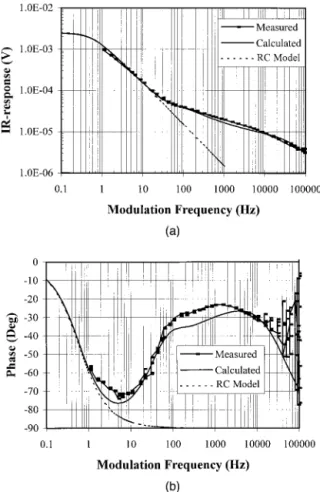
mate-Fig. 4. Response versus modulation frequency of the SrTiO3
sub-strate sample 064-01a at 80 K and 250-mA dc bias current.
Mea-sured and calculated共a兲 magnitude and 共b兲 phase of the response
from both the proposed model and the basic R-C model.
Fig. 5. Response versus modulation frequency of the LaAlO3
sub-strate sample 061-02a at 79.5 K and 500-mA bias current.
Mea-sured and calculated共a兲 magnitude and 共b兲 phase of response from both the proposed model and the basic R-C model.
rial neglected by the one dimensionality of the model. Hence, for a relatively low thermal-conductive sub-strate sample with a small ds兾A ratio, this factor is
expected to approach 1 as obtained for sample 061-02a. By use of the known parameters for the films and the substrates and the obtained values for the␣ and the boundary resistance, the phase and the mag-nitude of the response for the samples were calcu-lated and plotted in Figs. 4 – 6.
As shown in Figs. 4 – 6, at low modulation frequen-cies there is a discrepancy between the results from the model and the measured values. This discrep-ancy was found to increase by the increase of the thermal conductivity of the substrate materials, showing its maximum for the most conductive sub-strate material. This is also interpreted to be due to the one dimensionality of the model, ignoring the lateral heat diffusion in the substrate materials un-derneath the pattern. When the magnitudes of the response curves in Figs. 4, 5, and 6, for SrTiO3, LaAlO3, and MgO, respectively, are compared, the
discrepancy is the most for the most thermal-conductive MgO substrate sample 064-03a of this work. This is also consistent with the variation of␣, which is the highest for the same sample. It is pro-posed that this discrepancy be avoided by use of a three-dimensional solution for the model or use of an
approximate cylindrical solution for a truncated cone structure with a linearly increasing base from the film to the bottom of the substrate. Such approxi-mate solutions can also be applied with simulation programs such asSPICE, in which the parameters can
further be considered as frequency dependent.3 The
preceding alternative approaches that can be applied to any kind of bolometers are presently under way and will be presented elsewhere.
B. Phase of the Response and the High- and the Low-End-Frequency Behavior
The phase of the response of the samples was found to be much more sensitive to the values of the char-acteristic parameters of the samples. In particular, the drop of the phase at high-end-frequency response was the determining factor in finding the equivalent values of Cfand Rfsgiven in Table 1. Although the low-end calculated phase of the response is in good agreement with the experimental results for SrTiO3
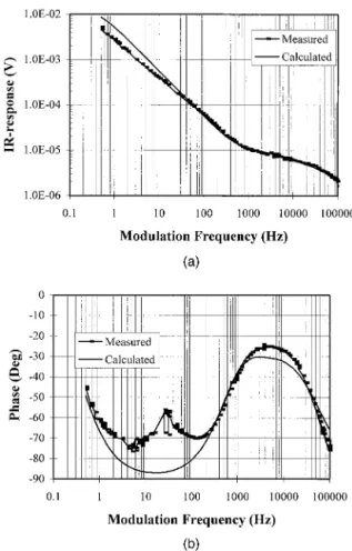
and LaAlO3substrate samples, there is a peak in the frequency range of 10 –100 Hz in the MgO substrate sample that cannot be explained by this model. This behavior was also observed for all other MgO sub-strate samples. This was found to occur at lower frequencies in thinner substrate samples, e.g., at ap-proximately 10 –20-Hz frequencies for 0.025-cm-thick MgO substrate samples compared with those of 0.5-cm-thick MgO substrate sample 064-03a shown in Fig. 6共b兲. One speculated mechanism for this is in-terpreted as possibly being due to the reflection and the interference effect of the acoustical phonons within the boundaries of the substrate underneath the superconducting pattern.14 The possible effect
of the superconducting material on the spectral pho-non density in the substrate and its consequent ef-fects have already been observed in the phase of the response versus temperature of the samples and are presented and discussed elsewhere.14
C. Midrange Frequency Behavior of the Phase and the Magnitude of the Response
There is a slight discrepancy in the midrange fre-quency response curves compared with that of the model. This is clearly seen in the plateau of the phase versus frequency curves for all the samples shown in Figs. 4 – 6. The discrepancy can also be seen partly in the magnitude of the response curves in the same frequency regime. The measured re-sponse in this range was found to be slightly higher in magnitude and more in phase with the radiation sig-nal than the expected values from the model.
The possible effect of the radiation absorption by the open areas of the substrate within the meander lines of the patterns was investigated as a possible source for the discrepancy. This consideration in the model led to a lower phase of the response in-creasing the observed discrepancy in the plateau re-gion of the phase curves, particularly for the SrTiO3
substrate sample. The spectral absorption of the crystalline substrate materials was also measured
Fig. 6. Response versus modulation frequency of the 0.5-cm-thick
MgO substrate sample 064-03a at 79 K and 1-mA bias current.
Measured and calculated共a兲 magnitude and 共b兲 phase of the
from 600 nm to 50m and was found to be approx-imately 12%, 20%, and 8% for the 0.05-cm-thick Sr-TiO3, LaAlO3, and MgO substrates, respectively, at
the 850-nm radiation wavelength. Although the ef-fect of the substrate absorption was found to be neg-ligible in the response of the samples measured at the 850-nm radiation wavelength, it was found to have a major effect on the measured spectral response of the samples at longer wavelengths.3,7,12,20,26 The effect
of the substrate absorption on the spectral response of the detectors in Table 1 was studied and reported elsewhere.7,12
A small and relatively fast component in the time response of the samples was observed and found to increase relatively compared with the total response as the modulation frequency increased. This could not be explained by the thermal response as modeled in this paper. The steady-state time response of Sr-TiO3 substrate sample 064-01a in the
above-mentioned frequency regime is shown in Fig. 7. As observed from the figure, there exist an abrupt jump and drop at the edge of the on and off switching times of the radiation source. The source is a fast near-IR source that is derived by a square-wave voltage sig-nal, as explained in Section 2. The same type of the steady-state time response is observed for all other samples in the same frequency regime. The effect of this fast component of the response is in favor of the discrepancy 共i.e., lowering the phase value and in-creasing the magnitude of the response from those values calculated by the model兲. This is interpreted as the nonthermal component of the response and is a possible source for the discrepancy, which needs to be further investigated.
5. Summary and Conclusions
The phase and the magnitude of response versus modulation frequency of superconducting edge-transition bolometers were shown to be strongly a function of the thermal boundary resistance at the film–substrate and the substrate– holder interfaces. A one-dimensional model based on the above facts is proposed for bolometers with superconducting film patterns larger than or comparable with the
sub-strate thickness. The model, while being a useful tool for design optimizations for such devices, could also be used to monitor the thermal parameters of the detectors. The results from the model confirm the major effects of the thermal boundary resistance’s dominating the effects of the substrate materials at low- and high-end modulation frequencies. The ob-tained thermal boundary resistance at the substrate– holder of the studied samples was found to be the limiting factor at the dc or low modulation frequen-cies.
A good fit between both the measured magnitude and the phase of the response to that obtained from the model could be obtained for the samples from very low modulation frequencies of 0.5 Hz up to⬃100 kHz, the limits of the setup. The fit matched the best for the SrTiO3substrate sample compared with that for the MgO and the LaAlO3 substrates. From the
high-frequency end of the response, the supercon-ducting film–substrate thermal boundary resistance and the heat capacity of the films could be obtained. Both the film–substrate boundary resistance and the superconducting film heat capacity of the samples in this paper were found to be larger than the previously typical reported values in the literature. From the model and from the low and the midrange frequen-cies of the response, the heat capacity and the ther-mal conductivity of the used substrate materials 共SrTiO3, MgO, and LaAlO3兲 and the substrate–
holder thermal boundary resistance could also be ob-tained. The obtained thermal parameters of the substrate materials agree well with the values pre-viously reported in the literature.
In conclusion, the proposed one-dimensional ther-mal model can be used to monitor the therther-mal pa-rameters of the superconducting film, substrate, and the thermal boundary resistance values of an edge-transition superconductive bolometer. Also, the mechanism of heat flow caused by the absorbed ra-diation in the samples can be investigated by use of the results from the model in this kind of device. The response versus modulation frequency of the bo-lometers was found to be the most informative data in this respect. The response of the bolometers with large superconducting pattern areas compared with the substrate thickness was found to be mainly bolo-metric at low and midrange modulation frequencies when following the results from the proposed model. Consideration of a three-dimensional solution to the model would be required for further accurate re-sponse analysis of samples with small superconduct-ing pattern areas compared with the substrate thickness.
References
1. P. E. Phelan, “Thermal response of thin-film high-Tc
supercon-ductors to modulated irradiation,” J. Therm. Phys. Heat Transfer 9, 397– 402共1995兲.
2. S. Zeuner, W. Prettl, and H. Lengfellner, “Fast thermoelectric response of normal state YBa2Cu3O7⫺d films,” Appl. Phys.
Lett. 66, 1833–1835共1995兲.
3. M. Fardmanesh, A. Rothwarf, and K. J. Scoles, “Low and
Fig. 7. Steady-state response versus time of SrTiO3 substrate
sample 064-01a at the 560-mA bias current, radiated by a 20-Hz
midrange modulation frequency response for YBCO infrared detectors: interface effects on the amplitude and phase,” IEEE Trans. Appl. Supercond. 5, 7–13共1995兲.
4. M. Nahum, S. Verghese, and P. L. Richards, “Thermal bound-ary resistance for YBa2Cu3O7⫺xfilms,” Appl. Phys. Lett. 59,
2034 –2036共1991兲.
5. A. V. Sergeev, A. D. Semenov, P. Kouminov, V. Trifonov, I. G. Goghize, B. S. Karasik, G. N. Gol’tsman, and E. M. Gershen-zon, “Transparency of a YBa2Cu3O7-film兾substrate interface
for thermal phonons measured by means of voltage response to radiation,” Phys. Rev. B 49, 9091–9096共1994兲.
6. C. D. Marshal, I. M. Fishman, R. C. Dorfman, C. B. Eom, and M. D. Fayer, “Thermal diffusion, interfacial thermal barrier, and ultrasonic propagation in YBa2Cu3O7⫺x thin films:
surface-selective transient-grating experiments,” Phys. Rev. B
45, 10009 –10021共1992兲.
7. M. Fardmanesh, K. J. Scoles, and A. Rothwarf, “Control of the responsivity and the detectivity of superconductive edge-transition YBa2Cu3O7⫺xbolometers through substrate
prop-erties,” Appl. Opt. 38, 4735– 4742共1999兲.
8. K. Fushinobu, P. E. Phelan, K. Hijikata, T. Nagasaki, and M. I. Flik, “Thermal analysis of the performance of a high-Tc
super-conducting bolometer,” J. Heat Transfer 116, 275–279共1994兲. 9. A. Frenkel, “Mechanism of nonequilibrium optical response of high-temperature superconductors,” Phys. Rev. B 48, 9717– 9725共1993兲.
10. H. Neff, “Modeling and optimization of high-Tc
superconduct-ing bolometers: the effect of film thickness,” J. Appl. Phys.
69, 8375– 8379共1991兲.
11. M. I. Flik, P. E. Phelan, and C. L. Tien, “Thermal model for the bolometric response of high-Tcsuperconducting films to optical
pulses,” Cryogenics 30, 1118 –1128共1990兲.
12. M. Fardmanesh, A. Rothwarf, and K. J. Scoles, “The respon-sivity and detectivity limits for patterned YBa2Cu3O7⫺x
super-conductive IR-detectors,” in Proceedings of the Sixth International Superconductive Electronics Conference, H. Kock and S. Knappe, eds.共Physikaisch-Technidsche Bundesanstalt, Berlin, 1997兲, Vol. 3, pp. 399–401.
13. M. Fardmanesh, K. J. Scoles, and A. Rothwarf, “DC charac-teristics of patterned YBa2Cu3O7⫺xsuperconducting thin film
bolometers: artifacts related to joule heating, ambient pres-sure, and microstructure,” IEEE Trans. Appl. Supercond. 8, 69 –78共1998兲.
14. M. Fardmanesh, A. Rothwarf, and K. J. Scoles, “YBa2Cu3O7⫺x
infrared bolometers: temperature dependent responsivity and deviations from the dR兾dT curve,” J. Appl. Phys. 77, 4568 – 4575共1995兲.
15. A. Jahanzeb, C. M. Travers, Z. Celik-Butler, and D. P. Butler, “A semiconductor YBaCuO microbolometer for room temper-ature IR imaging,” IEEE Trans. Electron Devices 44, 1795– 1801共1997兲.
16. C. M. Travers, A. Jahanzeb, D. P. Butler, and Z. Celik-Butler, “Fabrication of semiconducting YBaCuO surface-micromachined bolometer arrays,” J. Microelectromech. Syst. 6, 271–276共1997兲.
17. M. Fardmanesh, M. Ihsan, A. Rothwarf, K. Scoles, and K. Pourrezaei, “Thick and thin film Y–Ba–Cu–O infrared detec-tors,” AIP Conf. Proc. 251, 681– 691共1991兲.
18. M. Nahum, Q. Hu, P. L. Richards, S. A. Sachtjen, N. Newman, and B. F. Cole, “Fabrication and measurement of high Tc
superconducting bolometers,” IEEE Trans. Magn. 27, 3081– 3084共1991兲.
19. P. L. Richards, J. Clarke, R. Leoni, Ph. Lerch, S. Verghese, M. R. Beasley, T. H. Geballe, R. H. Hammond, P. Rosenthal, and S. R. Spielman, “Feasibility of the high T superconducting bolometer,” Appl. Phys. Lett. 54, 283–285共1989兲.
20. M. Fardmanesh, A. Rothwarf, and K. J. Scoles, “Noise char-acteristics and detectivity of YBa2Cu3O7superconducting
bo-lometers: bias current, frequency, and temperature dependence,” J. Appl. Phys. 79, 2006 –2011共1996兲.
21. H. Chou, H. Z. Chen, M. T. Hong, Y. C. Chen, and T. C. Chow, “Bolometric detection in a precipitation free YBa2Cu3O7⫺xfilm
at 77 K,” Appl. Phys. Lett. 68, 2741–2743共1996兲.
22. J. H. Hao, F. Q. Zhou, X. R. Zhao, H. D. Sun, X. J. Yi, and Z. G. Li, “Responsitivity calculation and measurement of YBaCuO optical detector,” IEEE Trans. Appl. Supercond. 3, 2167–2169 共1993兲.
23. G. D. Poulin, J. Lachapelle, S. H. Moffat, F. A. Hegmann, and J. S. Preston, “Current-voltage characteristics of dc voltage biased high temperature superconducting microbridges,” Appl. Phys. Lett. 66, 2576 –2578共1995兲.
24. K. D. Irwin, G. C. Hilton, D. A. Wollman, and J. M. Martinis, “X-ray detection using a superconducting transition-edge sen-sor microcalorimeter with electrothermal feedback,” Appl. Phys. Lett. 69, 1945–1947共1996兲.
25. Z. M. Zhang and A. Frenkel, “Thermal and nonequilibrium responses of superconductors for radiation detectors,” J. Supercond. 7, 871– 883共1994兲.
26. K. Kamaras, K. L. Barth, F. Keilmann, R. Henn, M. Reedyk, C. Thomsen, M. Cardona, J. Kircher, P. L. Richards, and J. L. Stehle, “The low-temperature infrared optical functions of Sr-TiO determined by reflectance spectroscopy and spectroscopic ellipsometry,” J. Appl. Phys. 78, 1235–1240共1995兲.