Testing Ourselves
Levent Sevgi
Electrical & Computer Engineering Dept. University of Massachusetts Lowell Lowell, MA 01854 USA
Tel: +1 (978) 934-3572; +1 (978) 852-8043 E-mail: [email protected]
http://www3.dogus.edu.tr/lsevgi
T
he tutorials we have published in this column and the MATLAB scripts and packages we have shared with the readers have been used all around the world. We’re encour aged a lot by the positive feedback we have received. I’m glad to inform you that most of those tutorials and simulation codes/ virtual tools are being revised and harmonized with sig nifi cant new material for my new book, Electromagnetic Modeling and Simulation (EM ModSim). This will be pub lished by the IEEE Press/Wiley as part of the IEEE Press Series on Electromagnetic Wave Theory with AP-S sponsor ship. The book will be on the market around June 2013, and will most probably be ready for the AP-S Orlando meeting. Thanks to all the IEEE and Wiley reviewers: their full support was very important in fi nalizing this book.I’ve taught EM ModSim as a graduate-level course at Doğuş University for several years. I proposed and taught it here in UMASS Lowell last semester. I have also organized
New Memristor Applications:
AM, ASK, FSK, and BPSK Modulators
İ. Cem Göknar, Fatih Öncül, and Elham Minayi
Department of Electronics and Communications EngineeringDogus University, Istanbul, Turkey E-mail: [cgoknar, eminayi]@dogus.edu.tr
Abstract
Implementations of amplitude (AM), amplitude-shift keying (ASK), frequency-shift keying (FSK), and binary phase-shift keying (BPSK) modulators with memristors are presented as new applications. The proposed modulators operate in current mode. They contain a preprocessing circuit that converts unipolar bit sequences into an appropriate form for modulation with at most two memristors. Using the memristor model developed by Biolek et al., PSPICE simulations of the proposed modulators that verify the mathematical derivations are presented.
Keywords: Memristor; amplitude shift keying (ASK); frequency shift keying (FSK); binary phase shift keying (BPSK) several short courses and seminars on this topic in nearly a dozen countries. The last one was at ACES 2013, Monterey, in March 2013. The book is the product of all those studies and publications of more than a decade.
Radiowave propagation models have long been used in electromagnetic signal-prediction problems. Different models use different sources: normalized results have therefore usu-ally been compared. Normalization has been done against maximum values, free-space values, or values obtained above a non-penetrable fl at Earth. This is practical and acceptable in long-range propagation modeling, because excitation differ-ences become negligible. Today’s interest and priorities in propagation modeling have shifted to quite short ranges, which necessitates accurate source modeling. ModSim chal lenges and accurate source modeling will be discussed in this column in the next issue, with several useful MATLAB codes.
1. Introduction
I
n 1971, using the missing fourth link between the fl ux and the charge, Leon Chua postulated a new element that he named a “memristor,” (a short form of “MEMory ResISTOR”). This was identifi ed by benefi ting from the rules of symmetry [1]. It was brought to the attention of the Anten nas and Propagation Society with the article in [2]. In 2008, 37 years after it was postulated, HP scientists published a paper announcing the physical realization of the memristor as a sim ple two-terminal element. They thus built a bridge between memristor theories and applications [3]. With this realization and its mathematical model provided by HP, new investiga tions and publications about the applications of the memristor to traditional as well as new circuit structures surfaced. Although the memristor – an analog device by its nature – is popular for nonvolatile memory applications, some approaches to modulation techniques with a memristor have also been considered. There are very few papers about its use in communications [4, 5]. Applications of the memristor’s properties to other types of modulators, oscillators, and fi lters can be found in [6].In this paper, amplitude-shift-keying, frequency-shift-keying, and binary-phase-shift-keying modulators with very simple architectures are proposed. These contain a preproc-essing block and one of HP’s TiO2 memristor for amplitude-shift keying, and two of HP’s TiO2 memristors for frequency-shift keying and binary phase-frequency-shift keying. The amplitude-modulation modulator was the subject of the quiz, with its answer given at the end of the paper. The need for using a preprocessing block arises for converting unipolar bit sequences to an appropriate form for storing the data in the memristor as its memristance. The mathematical analyses and their verifi cations via simulations are also presented.
2. Fundamentals of the Memristor
As introduced in [1], the memristor is a circuit element that is characterized by an algebraic relationship between the fl ux, ϕ, and the charge, q, as follows:
(
,)
0f q ϕ = . (1)
If a memristor that is identifi ed by the relation of Equation (1) is charge controlled, then the relationship becomes
( )
f q
ϕ = . (2)
Assuming a differentiable f, and applying the chain rule gives
( )
d t( )
df q dq( )
( ) ( )
v t M q t i t
dt dq dt
ϕ
= = = , (3)
where M is called the memristance, and has units of Ω. Rewriting Equation (3) in terms of the current,
( )
0 0t( )
( )
v t =M q + i τ τd i t
∫
, (4)showing the dependence of the memristance on the history of the current through it. The voltage at time t depends on the values of the current from time t =0 on, and the initial charge,
0
q , justifying the use of “memory” in the name of the component.
A memristor shows one of its special behaviors with its voltage-current characteristic. Its current will be zero if and only if its voltage is zero. If a sinusoidal current is applied to the memristor, the current-voltage characteristic will show a hysteresis effect, also called a Lissajous curve, as shown in Figure 1. The memristance is affected by the frequency of the applied periodic signal, which is another of the memristor’s “fi ngerprints.” For a sinusoidal current, Equation (4) becomes
( )
0 1 0sin( )
0cos( )
v t M q I ωt I ωt ω = + . (5)Increasing the excitation frequency causes a shrinking in the hysteresis loop, because of the factor 1 ω. With increasing frequency, the shrinking continues, and at very high frequen-cies, the memristor practically behaves like a linear resistor with value M q
( )
, as set by the initial charge. This behavior will be the key property of the memristor in the following applications.3.HP’s
TiO
2Memristor
In 2008, Strukov et al. created a TiO2 two-terminal memristor prototype. This was almost as simple as an ordinary resistor. It showed a switching behavior similar to Chua’s memristor, with a model as described in [3]. In this memristor,
Figure 1. The v-i Lissajous curves for frequencies ω1, ω2
a very thin fi lm of titanium dioxide (TiO2) is sandwiched between two platinum (Pt) contacts, and one side of the TiO2 is doped with oxygen vacancies. Undoped TiO2 is a high-resistance semiconductor. With doping, oxygen vacancies make the TiO2 material conductive. Strukov et al. revealed some fundamental defi ning equations for this memristor, without pointing out that the dopant drift slows down near the Pt contacts because of the boundary effects. The voltage-cur rent relationship of HP’s memristor is given by
( )
ONW t( )
OFF 1 W t( ) ( )
v t R R i t D D = + − , (6a)( )
( )
for 0( )
0 otherwise v ONR dW t i t W t D D dt µ ≤ ≤ = . (6b)The memristance thus becomes
( )
ON W t( )
OFF 1 W t( )
M W t R R D D = + + − . (6c)Here, the values for µv and D are 10−14cm s V2 1− −1 and 10 nm, respectively, with RON =10Ω, ROFF =10kΩ.
In Equation (6), D is the “length” of the titanium-dioxide fi lm, w is the “thickness” of the doped enlargeable region, RON
is the “on-state” available minimum resistance, ROFF is the “off-state” available maximum resistance, q t
( )
is the total charge passing through the memristive device, and µv is the “average drift velocity” or “migration coeffi cient.”Integrating both sides of Equation (6b) gives
( )
min{
( ) ( )
,}
W t = f t u W D , (7)
where u
( )
is the unit step function, and( )
0 v ONR( )
f t W q t
D
µ
= + . (8)
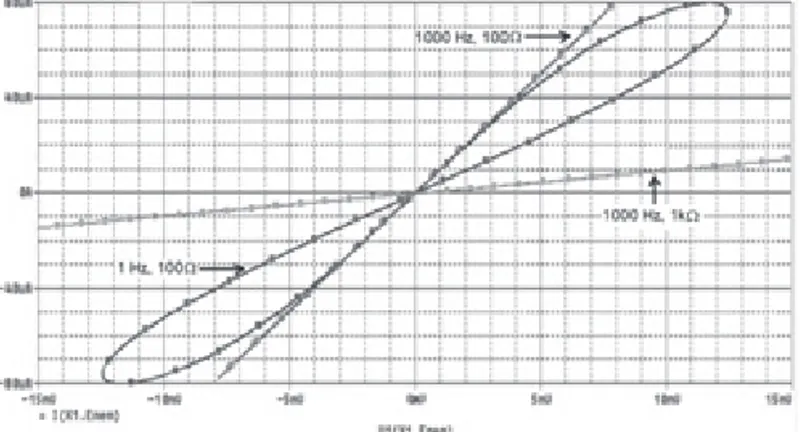
Based on the equalities of Equations (6) and (7), a SPICE model for HP’s TiO2 memristor with nonlinear dopant drift was given in [7]. Three different sinusoidal signals were applied to this model with different initial conditions, and the outcomes are shown in Figure 2. The hysteresis loop was gen erated at 1 Hz, with 100 Ω initial memristance. The linear characteristic with smaller slope was obtained for a 1 kΩ ini tial memristance, with a larger slope for 100 Ω initial memris tance, both at 1 kHz. This behavior indicated that the mem ristor could be used as a linear resistance at high frequencies with memristance values set by the initial charge. All of the signature properties of the memristor were hence satisfi ed.
4. Amplitude-Shift-Keying Modulator
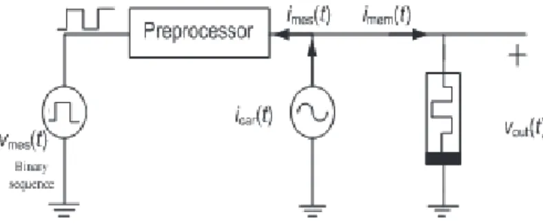
Taking advantage of the memristor’s switching mecha-nism, it is possible to implement amplitude-shift-keying, fre-quency-shift-keying, and binary-phase-shift-keying modula-tors. The advantage of the high frequency behavior of the memristor, which was explained in Section 2 with Equa-tion (5), will again be exploited. However, in order to operate the switching mechanism, there is a need for a “preprocess-ing” stage in these modulators that can convert the unipolar bit sequence into the appropriate form for modulation with the memristor.
If the baseband signal is directly applied to the circuit, the state of memristance is settled to a value, and does not change its state for a changing bit sequence. The preprocess ing circuit can be implemented simply with a DSP (digital signal processor) or with the circuit shown in Figure 3. This simple circuit is made of a voltage-controlled current source (VCCS) and a differentiator, which consists of an RC circuit that recognizes the state changes from 0 to 1 or 1 to 0. The voltage at the output of the differentiator in Figure 3b can be expressed as
( )
( )
( )
0 1RCs V s V s RCsV s RCs = ≅ + for 1 RC ω . (9) The SPICE simulation results for the input baseband signal and the output current of the preprocessing block are shown in Figures 4a and 4b, respectively.A voltage-controlled current source or its equivalent is needed to convert the output voltage of the differentiator to the current that controls the state of the memristor. One bit of the binary signal, v t
( )
, as illustrated in Figure 5, and its output current form from the preprocessor, can be expressed asFigure 2. Plots of current as a function of voltage for sinu-soidal signals applied to a memristor with different initial memristances.
Figure 3. The preprocessing circuit: (a) conceptual, (b) a schematic.
Figure 4. (a) The baseband input signal, (b) the output current, i t
( )
.Figure 5. (a) One bit of the binary signal, (b) the output current.
a very thin fi lm of titanium dioxide (TiO2) is sandwiched between two platinum (Pt) contacts, and one side of the TiO2 is doped with oxygen vacancies. Undoped TiO2 is a high-resistance semiconductor. With doping, oxygen vacancies make the TiO2 material conductive. Strukov et al. revealed some fundamental defi ning equations for this memristor, without pointing out that the dopant drift slows down near the Pt contacts because of the boundary effects. The voltage-cur rent relationship of HP’s memristor is given by
( )
ONW t( )
OFF 1 W t( ) ( )
v t R R i t D D = + − , (6a)( )
( )
for 0( )
0 otherwise v ONR dW t i t W t D D dt µ ≤ ≤ = . (6b)The memristance thus becomes
( )
ON W t( )
OFF 1 W t( )
M W t R R D D = + + − . (6c)Here, the values for µv and D are 10−14cm s V2 1− −1 and 10 nm, respectively, with RON =10Ω, ROFF =10kΩ.
In Equation (6), D is the “length” of the titanium-dioxide fi lm, w is the “thickness” of the doped enlargeable region, RON
is the “on-state” available minimum resistance, ROFF is the “off-state” available maximum resistance, q t
( )
is the total charge passing through the memristive device, and µv is the “average drift velocity” or “migration coeffi cient.”Integrating both sides of Equation (6b) gives
( )
min{
( ) ( )
,}
W t = f t u W D , (7)
where u
( )
is the unit step function, and( )
0 v ONR( )
f t W q t
D
µ
= + . (8)
Based on the equalities of Equations (6) and (7), a SPICE model for HP’s TiO2 memristor with nonlinear dopant drift was given in [7]. Three different sinusoidal signals were applied to this model with different initial conditions, and the outcomes are shown in Figure 2. The hysteresis loop was gen erated at 1 Hz, with 100 Ω initial memristance. The linear characteristic with smaller slope was obtained for a 1 kΩ ini tial memristance, with a larger slope for 100 Ω initial memris tance, both at 1 kHz. This behavior indicated that the mem ristor could be used as a linear resistance at high frequencies with memristance values set by the initial charge. All of the signature properties of the memristor were hence satisfi ed.
4. Amplitude-Shift-Keying Modulator
Taking advantage of the memristor’s switching mecha-nism, it is possible to implement amplitude-shift-keying, fre-quency-shift-keying, and binary-phase-shift-keying modula-tors. The advantage of the high frequency behavior of the memristor, which was explained in Section 2 with Equa-tion (5), will again be exploited. However, in order to operate the switching mechanism, there is a need for a “preprocess-ing” stage in these modulators that can convert the unipolar bit sequence into the appropriate form for modulation with the memristor.
If the baseband signal is directly applied to the circuit, the state of memristance is settled to a value, and does not change its state for a changing bit sequence. The preprocess ing circuit can be implemented simply with a DSP (digital signal processor) or with the circuit shown in Figure 3. This simple circuit is made of a voltage-controlled current source (VCCS) and a differentiator, which consists of an RC circuit that recognizes the state changes from 0 to 1 or 1 to 0. The voltage at the output of the differentiator in Figure 3b can be expressed as
( )
( )
( )
0 1RCs V s V s RCsV s RCs = ≅ + for 1 RC ω . (9) The SPICE simulation results for the input baseband signal and the output current of the preprocessing block are shown in Figures 4a and 4b, respectively.A voltage-controlled current source or its equivalent is needed to convert the output voltage of the differentiator to the current that controls the state of the memristor. One bit of the binary signal, v t
( )
, as illustrated in Figure 5, and its output current form from the preprocessor, can be expressed asFigure 2. Plots of current as a function of voltage for sinu-soidal signals applied to a memristor with different initial memristances.
Figure 3. The preprocessing circuit: (a) conceptual, (b) a schematic.
Figure 4. (a) The baseband input signal, (b) the output current, i t
( )
.Figure 5. (a) One bit of the binary signal, (b) the output current.
( )
1 1 2 2 3 3 4 0 0 At t t V t t t v t V At t t t t t t ≤ < ≤ < = − ≤ < ≤ < , (10)( )
1 1 2 2 3 3 4 0 0 0 A t t t t t i t A t t t t t t ≤ < ≤ < = − ≤ < ≤ < ,where A is the amplitude of the current at the output of the voltage-controlled current source. W t
( )
is therefore found as( )
(
)
(
)
0 1 1 0 1 2 1 0 2 2 3 1 0 3 2 3 4 0 KAt W t t KAt W t t t W t KAt W KA t t t t t KAt W KA t t t t t + ≤ ≤ + ≤ ≤ = + − − ≤ ≤ + − − ≤ ≤ , (11a) which settles at( )
3 0 1(
3 2)
0 W t =W +AKt −AK t −t =W (11b) for a pulse width of T, T t= = −1 t3 t2, with K=µv ONR D.The nonlinearity of Equation (6b) imposes a restriction on the product AT of the pulse that drives the memristor for Equations (11) to hold, and hence for proper operation. To guarantee the condition wOFF ≤w t
( )
≤wON, using Equa-tion (11a), WOFF ≤KAt W1+ 0≤WON, which yields0 0 OFF ON W W W W AT K K − − ≤ ≤ . (11c)
The boundary condition wOFF ≤KAT w+ 0−KAT w≤ ON
yields wOFF ≤w0≤wON, which is no restriction. In fact, the expressions in Equation (11b) show that after an applied pulse of time duration T, if another pulse – opposite in sign but of the same magnitude and duration – is applied, the width, w, turns back to its initial value, w0, at time t3. The memristor preserves one of the high or low states as memristance. The narrow stimuli that are converted from a unipolar binary base band signal by the preprocessor block can change the mem ristance state, due to the sign or the direction of the current. The multiplication of carrier current with the higher memris tance value reached yields an acceptable output voltage. The amplitude-shift-keying modulator with a single memristor is shown in Figure 6.
The change of memristance is expressed in Equation (12) for the given sample bit sequence of Figure 5 (observe the current directions), and using the expression in Equation (10) for t t≥ 3: M W t
( )
=M W{
0 1( )
3( )
( )
2 0 0 t t tmes t mes car
K i τ τd i τ τd i τ τ d
+ − +
∫
∫
∫
.(12)
If ωcar ωmes, the settlement of width W t
( )
for t t≥ 3 is( )
1 3(
)
2
0 mes 0t mes tt car sin car car I W t W K i τ i τ ω t ω = + − + + . (13)
Neglecting the effect of the high-frequency carrier signal because ωcar is very large compared to ωmes, one obtains for
0 ON
W =W (which WON covers the maximum allowed conduc-tive region) the minimum memristor resistance, RON.
The voltage at the output of the memristor is given in Equation (14):
( )
(
(
)
(
)
)
(
)
1 23 4
cos cos
ON mes car car out ON car car M W KI T I t t t t v t M W I t t t t ω ω − ≤ ≤ = ≤ ≤ . (14)
The SPICE simulation results shown in Figure 7 were obtained by using the memristor model given in [6], with parameter values RON =10Ω, ROFF =10 kΩ, and Rinit =20Ω. The nonlinear dopant drift was modeled via the Joglekar window with the parameter P =10. The message was as shown in Figure 7a: the carrier signal had an amplitude of 1 mA and a frequency of 1000 Hz. The memristance value became almost
2 kΩ. The output voltage was approximately 20 mV while the binary state was zero. It increased up to 2 V while the binary state was one.
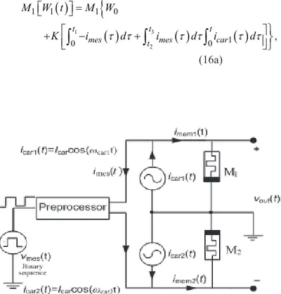
5. Frequency-Shift-Keying Modulator
As mentioned before, the switching mechanism of the memristor can be used to produce ON or OFF states of a base-band signal. A frequency-shift-keying modulator with two
Figure 6. An amplitude-shift-keying modulator using a single memristor.
memristors can therefore be designed by taking advantage of the high-frequency behavior of the memristor.
In order to set the states of the memristor, the preproces sor converts the unipolar binary-message signal to the special form depicted in Figure 8. Each carrier signal (icar1
( )
t and icar2( )
t ) has a high enough value in frequency in order to keep the memristance values unaltered, and to produce the following at the output:( )
(
1)
for binary input0 otherwise
car out ASin t v t = ω
, (15a)
( )
(
2)
for binary input0 otherwise
car out ASin t v t = ω
, (15b)
with the frequency condition of ωcar1≠ωcar2.
The proposed frequency-shift-keying modulator circuit with two memristors is shown in Figure 8. The two memris-tors are needed to produce two output signals with different carrier frequencies. It should be observed that the memristors are connected with each other in opposite polarities. With this confi guration, the memristance of one memristor increases while the other memristance decreases. The output current of the preprocessor alternates the memristances between the high and low states. The message signal positively supplies one of the memristors to set its state to a low memristance, while the other signal is supplied negatively to have its memristance set at high state, or vice versa. As mentioned in amplitude-shift-keying modulation, at the low-memristance state, the voltage of that memristor will be low. If the memristance is high, its voltage will be dominantly high. In this case, this implies that only one memristor is responsible for producing the output at time duration of each binary bit. Hence, the expressions given by Equations (10) and (11) cover the principles of frequency-shift-keying modulation.
The settled memristance value is multiplied by the cur rent of the carrier signal in order to produce the output volt age. The memristors preserve their states as memristances. At the output, the voltage on one of the memristors is close to zero, so one of the modulated signals is suppressed, while the other signal appears as a voltage that is the multiplication of the current signal and the memristance. As a result, the carri ers at different frequencies can be modulated with two mem ristors by storing the binary states as memristances.
The change of memristance is expressed in Equation (16) for the given sample bit sequence of Figure 5a, as implied by Equations (10) and (11).
( )
{
1 1 1 0 M W t =M W 1( )
3( )
( )
2 1 0 0 t t tmes t mes car
K i τ τd i τ τd i τ τ d
+ − +
∫
∫
∫
,(16a)
Figure 7. The PSPICE simulation plots of the amplitude-shift-keying memristor modulator: (a) the unipolar binary sequence, (b) the change of memristance, (c) the output of the amplitude-shift-keying modulator.
Figure 8. A frequency-shift-keying modulator using two memristors.
( )
1 1 2 2 3 3 4 0 0 At t t V t t t v t V At t t t t t t ≤ < ≤ < = − ≤ < ≤ < , (10)( )
1 1 2 2 3 3 4 0 0 0 A t t t t t i t A t t t t t t ≤ < ≤ < = − ≤ < ≤ < ,where A is the amplitude of the current at the output of the voltage-controlled current source. W t
( )
is therefore found as( )
(
)
(
)
0 1 1 0 1 2 1 0 2 2 3 1 0 3 2 3 4 0 KAt W t t KAt W t t t W t KAt W KA t t t t t KAt W KA t t t t t + ≤ ≤ + ≤ ≤ = + − − ≤ ≤ + − − ≤ ≤ , (11a) which settles at( )
3 0 1(
3 2)
0 W t =W +AKt −AK t −t =W (11b) for a pulse width of T, T t= = −1 t3 t2, with K=µv ONR D.The nonlinearity of Equation (6b) imposes a restriction on the product AT of the pulse that drives the memristor for Equations (11) to hold, and hence for proper operation. To guarantee the condition wOFF ≤w t
( )
≤wON, using Equa-tion (11a), WOFF ≤KAt W1+ 0≤WON, which yields0 0 OFF ON W W W W AT K K − − ≤ ≤ . (11c)
The boundary condition wOFF ≤KAT w+ 0−KAT w≤ ON
yields wOFF ≤w0≤wON, which is no restriction. In fact, the expressions in Equation (11b) show that after an applied pulse of time duration T, if another pulse – opposite in sign but of the same magnitude and duration – is applied, the width, w, turns back to its initial value, w0, at time t3. The memristor preserves one of the high or low states as memristance. The narrow stimuli that are converted from a unipolar binary base band signal by the preprocessor block can change the mem ristance state, due to the sign or the direction of the current. The multiplication of carrier current with the higher memris tance value reached yields an acceptable output voltage. The amplitude-shift-keying modulator with a single memristor is shown in Figure 6.
The change of memristance is expressed in Equation (12) for the given sample bit sequence of Figure 5 (observe the current directions), and using the expression in Equation (10) for t t≥ 3: M W t
( )
=M W{
0 1( )
3( )
( )
2 0 0 t t tmes t mes car
K i τ τd i τ τd i τ τ d
+ − +
∫
∫
∫
.(12)
If ωcar ωmes, the settlement of width W t
( )
for t t≥ 3 is( )
1 3(
)
2
0 mes 0t mes tt car sin car car I W t W K i τ i τ ω t ω = + − + + . (13)
Neglecting the effect of the high-frequency carrier signal because ωcar is very large compared to ωmes, one obtains for
0 ON
W =W (which WON covers the maximum allowed conduc-tive region) the minimum memristor resistance, RON.
The voltage at the output of the memristor is given in Equation (14):
( )
(
(
)
(
)
)
(
)
1 23 4
cos cos
ON mes car car out ON car car M W KI T I t t t t v t M W I t t t t ω ω − ≤ ≤ = ≤ ≤ . (14)
The SPICE simulation results shown in Figure 7 were obtained by using the memristor model given in [6], with parameter values RON =10Ω, ROFF =10 kΩ, and Rinit =20Ω. The nonlinear dopant drift was modeled via the Joglekar window with the parameter P =10. The message was as shown in Figure 7a: the carrier signal had an amplitude of 1 mA and a frequency of 1000 Hz. The memristance value became almost
2 kΩ. The output voltage was approximately 20 mV while the binary state was zero. It increased up to 2 V while the binary state was one.
5. Frequency-Shift-Keying Modulator
As mentioned before, the switching mechanism of the memristor can be used to produce ON or OFF states of a base-band signal. A frequency-shift-keying modulator with two
Figure 6. An amplitude-shift-keying modulator using a single memristor.
memristors can therefore be designed by taking advantage of the high-frequency behavior of the memristor.
In order to set the states of the memristor, the preproces sor converts the unipolar binary-message signal to the special form depicted in Figure 8. Each carrier signal (icar1
( )
t and icar2( )
t ) has a high enough value in frequency in order to keep the memristance values unaltered, and to produce the following at the output:( )
(
1)
for binary input0 otherwise
car out ASin t v t = ω
, (15a)
( )
(
2)
for binary input0 otherwise
car out ASin t v t = ω
, (15b)
with the frequency condition of ωcar1≠ωcar2.
The proposed frequency-shift-keying modulator circuit with two memristors is shown in Figure 8. The two memris-tors are needed to produce two output signals with different carrier frequencies. It should be observed that the memristors are connected with each other in opposite polarities. With this confi guration, the memristance of one memristor increases while the other memristance decreases. The output current of the preprocessor alternates the memristances between the high and low states. The message signal positively supplies one of the memristors to set its state to a low memristance, while the other signal is supplied negatively to have its memristance set at high state, or vice versa. As mentioned in amplitude-shift-keying modulation, at the low-memristance state, the voltage of that memristor will be low. If the memristance is high, its voltage will be dominantly high. In this case, this implies that only one memristor is responsible for producing the output at time duration of each binary bit. Hence, the expressions given by Equations (10) and (11) cover the principles of frequency-shift-keying modulation.
The settled memristance value is multiplied by the cur rent of the carrier signal in order to produce the output volt age. The memristors preserve their states as memristances. At the output, the voltage on one of the memristors is close to zero, so one of the modulated signals is suppressed, while the other signal appears as a voltage that is the multiplication of the current signal and the memristance. As a result, the carri ers at different frequencies can be modulated with two mem ristors by storing the binary states as memristances.
The change of memristance is expressed in Equation (16) for the given sample bit sequence of Figure 5a, as implied by Equations (10) and (11).
( )
{
1 1 1 0 M W t =M W 1( )
3( )
( )
2 1 0 0 t t tmes t mes car
K i τ τd i τ τd i τ τ d
+ − +
∫
∫
∫
,(16a)
Figure 7. The PSPICE simulation plots of the amplitude-shift-keying memristor modulator: (a) the unipolar binary sequence, (b) the change of memristance, (c) the output of the amplitude-shift-keying modulator.
Figure 8. A frequency-shift-keying modulator using two memristors.
( )
{
2 2 2 0 M W t =M W 1( )
3( )
( )
2 2 0 0 t t tmes t mes car
K i τ τd i τ τd i τ τ d
+ − +
∫
∫
∫
.(16b)
The settlement of the width, W t
( )
, is negligibly degenerated by the high-frequency condition, because both ωcar1 and ωcar2are very large compared to ωmes. Neglecting the effect of the high-frequency carrier signal, as was done in Equa tion (13), the settled widths are given in Equations (17a) and (17b) for memristors M1 and M2, respectively, for the initial width
0 ON W =W :
( )
1 2 1 3 4 , , ON mes ON W kI T t t t W t W t t t − ≤ ≤ = ≤ ≤ , (17a)( )
1 2 2 3 4 , , ON ON mes W t t t W t W kI T t t t ≤ ≤ = − ≤ ≤ . (17a)During time interval
[
t t1 2,]
, memristor M1 is highly resis tive, due to the narrow width, Equation (17a); the carrier sig nal (car1) appears at the output as a voltage with high magni tude, Equation (18a). In this case, M2 still keeps the initial memristance, RON, with the upper limit of width WON, Equa-tion (17b).During time interval
[
t t3 4,]
, the carrier signal (car1) produces a negligibly small voltage at the output, due to the highly conductive memristor M1 with the width turning backto the initial length and memristance RON as expressed in Equation (17a). However, in this case, the memristor M2 is highly resistive as defi ned in Equation (17b), and the carrier signal (car2) appears at the output as a higher voltage, Equa-tion (18b).
Each binary state can thus be modulated via two memris-tors by storing 1 bits with carrier signal (car1) on memristor
1
M , and 0 bits with carrier signal (car2) on memristor M2, as memristances.
( )
(
)
(
)
(
1)
1 31 42cos , cos ,
ON mes car car out ON car car M W kI T I t t t t V t MW I t t t t ω ω − ≤ ≤ = ≤ ≤ (18a)
( )
(
)
(
)
2(
2)
13 24 cos , I cos , ON car car outON mes car car
MW I t t t t V t M W kI T t t t t ω ω ≤ ≤ = − ≤ ≤ . (18b)
Restrictions similar to Equation (11c) also hold for the “Amplitude-Period product,” AT, of the pulses that drive the memristor.
The SPICE simulation results shown in Figure 9 were realized by using the memristor in [6], with parameter values of
10
ON
R = Ω, ROFF =10 kΩ, Rinit=20Ω for M1, and
10
ON
R = Ω, ROFF =10 kΩ, Rinit =2050Ω for M2. Nonlin-ear dopant drift was modeled via the Joglekar window with the parameter P =10. Sinusoidal carrier signals had an amplitude of 1 mA and a frequency of 1000 Hz forIcar1, and an amplitude of 1 mA and a frequency of 100 Hz forIcar2.
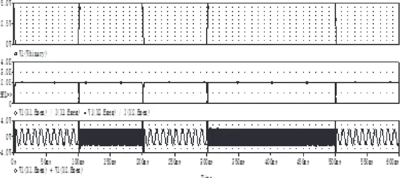
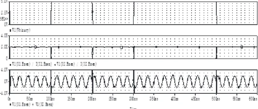
Figure 9. PSPICE simulation plots of the frequency-shift-keying memristor modulator: (a) the unipolar binary input, (b) the change of states of the memristance, (c) the output of the frequency-shift-keying modulator.
6. Binary-Phase-Shift-Keying Modulator
Binary-phase-shift-keying modulation can also be achieved using two memristors, because of their switching behavior. Furthermore, the circuit that was designed for fre-quency-shift-keying modulation is suitable for binary-phase-shift-keying generation by simply connecting a single carrier source instead of two, as shown in Figure 10. The operating principle of the circuit for binary-phase-shift-keying modula-tion using memristors is the same as the principle menmodula-tioned for frequency-shift keying. In frequency-shift keying, each memristor is responsible of storing one bit as a memristance at the time duration of each binary bit. Each memristor can be interpreted as implementing frequency-shift keying for differ-ently phased carrier signals at different times. The expressions mentioned in Equations (12) and (13) hence cover the princi-ples of binary-phase-shift-keying modulation.
The voltage at the output of the memristor is given in Equation (19):
( )
(
(
)
)
(
)
1 23 4
I cos , cos 0,
ON mes car car out ON car car M W kI T t t t t V t MW I t t t t ω ω − ≤ ≤ = ≈ ≤ ≤ (19a)
( )
(
(
)
)
(
)
1 2 3 4 cos 0, cos , ON car car outON mes car car
MW I t t t t V t M W kI T I t t t t ω ω ≈ ≤ ≤ = − ≤ ≤ (19b) These are obtained as follows.
For t1≤ ≤t t2, the memristor M1 is highly resistive, due to the narrow width, Equation (19a). The carrier signal,
( )
car
i t , produces the dominant output voltage, vout
( )
t , as expressed in Equation (19a). During this time interval, M2 still has the low initial memristance, RON, with the upper limit of width WON, Equation (17b).For t3≤ ≤t t4, the carrier signal, icar
( )
t , produces anegligibly small voltage at the output. This is due to the highly conductive state of memristor M1, which has memristance
ON
R , its width being back to the initial length as expressed in Equation (17a). However, in this case, the memristor M2 is highly resistive, as defi ned in Equation (17b). The carrier sig-nal, −imem
( )
t , now causes a detectable voltage with a minus sign at the output, as given in Equation (19b).Figure 11. The memristor binary-phase-shift-keying modulator’s PSPICE simulation plots: (a) the unipolar binary sequence, (b) the change of states of the memris tance, (c) the output of the frequency-shift-keying modula tor.
Figure 10. The binary-phase-shift-keying modulator using two memristors.
( )
{
2 2 2 0 M W t =M W 1( )
3( )
( )
2 2 0 0 t t tmes t mes car
K i τ τd i τ τd i τ τ d
+ − +
∫
∫
∫
.(16b)
The settlement of the width, W t
( )
, is negligibly degenerated by the high-frequency condition, because both ωcar1 and ωcar2are very large compared to ωmes. Neglecting the effect of the high-frequency carrier signal, as was done in Equa tion (13), the settled widths are given in Equations (17a) and (17b) for memristors M1 and M2, respectively, for the initial width
0 ON W =W :
( )
1 2 1 3 4 , , ON mes ON W kI T t t t W t W t t t − ≤ ≤ = ≤ ≤ , (17a)( )
1 2 2 3 4 , , ON ON mes W t t t W t W kI T t t t ≤ ≤ = − ≤ ≤ . (17a)During time interval
[
t t1 2,]
, memristor M1 is highly resis tive, due to the narrow width, Equation (17a); the carrier sig nal (car1) appears at the output as a voltage with high magni tude, Equation (18a). In this case, M2 still keeps the initial memristance, RON, with the upper limit of width WON, Equa-tion (17b).During time interval
[
t t3 4,]
, the carrier signal (car1) produces a negligibly small voltage at the output, due to the highly conductive memristor M1 with the width turning backto the initial length and memristance RON as expressed in Equation (17a). However, in this case, the memristor M2 is highly resistive as defi ned in Equation (17b), and the carrier signal (car2) appears at the output as a higher voltage, Equa-tion (18b).
Each binary state can thus be modulated via two memris-tors by storing 1 bits with carrier signal (car1) on memristor
1
M , and 0 bits with carrier signal (car2) on memristor M2, as memristances.
( )
(
)
(
)
(
1)
1 31 42cos , cos ,
ON mes car car out ON car car M W kI T I t t t t V t MW I t t t t ω ω − ≤ ≤ = ≤ ≤ (18a)
( )
(
)
(
)
2(
2)
13 24 cos , I cos , ON car car outON mes car car
MW I t t t t V t M W kI T t t t t ω ω ≤ ≤ = − ≤ ≤ . (18b)
Restrictions similar to Equation (11c) also hold for the “Amplitude-Period product,” AT, of the pulses that drive the memristor.
The SPICE simulation results shown in Figure 9 were realized by using the memristor in [6], with parameter values of
10
ON
R = Ω, ROFF =10 kΩ, Rinit=20Ω for M1, and
10
ON
R = Ω, ROFF =10 kΩ, Rinit =2050Ω for M2. Nonlin-ear dopant drift was modeled via the Joglekar window with the parameter P =10. Sinusoidal carrier signals had an amplitude of 1 mA and a frequency of 1000 Hz forIcar1, and an amplitude of 1 mA and a frequency of 100 Hz forIcar2.
Figure 9. PSPICE simulation plots of the frequency-shift-keying memristor modulator: (a) the unipolar binary input, (b) the change of states of the memristance, (c) the output of the frequency-shift-keying modulator.
6. Binary-Phase-Shift-Keying Modulator
Binary-phase-shift-keying modulation can also be achieved using two memristors, because of their switching behavior. Furthermore, the circuit that was designed for fre-quency-shift-keying modulation is suitable for binary-phase-shift-keying generation by simply connecting a single carrier source instead of two, as shown in Figure 10. The operating principle of the circuit for binary-phase-shift-keying modula-tion using memristors is the same as the principle menmodula-tioned for frequency-shift keying. In frequency-shift keying, each memristor is responsible of storing one bit as a memristance at the time duration of each binary bit. Each memristor can be interpreted as implementing frequency-shift keying for differ-ently phased carrier signals at different times. The expressions mentioned in Equations (12) and (13) hence cover the princi-ples of binary-phase-shift-keying modulation.
The voltage at the output of the memristor is given in Equation (19):
( )
(
(
)
)
(
)
1 23 4
I cos , cos 0,
ON mes car car out ON car car M W kI T t t t t V t MW I t t t t ω ω − ≤ ≤ = ≈ ≤ ≤ (19a)
( )
(
(
)
)
(
)
1 2 3 4 cos 0, cos , ON car car outON mes car car
MW I t t t t V t M W kI T I t t t t ω ω ≈ ≤ ≤ = − ≤ ≤ (19b) These are obtained as follows.
For t1≤ ≤t t2, the memristor M1 is highly resistive, due to the narrow width, Equation (19a). The carrier signal,
( )
car
i t , produces the dominant output voltage, vout
( )
t , as expressed in Equation (19a). During this time interval, M2 still has the low initial memristance, RON, with the upper limit of width WON, Equation (17b).For t3≤ ≤t t4, the carrier signal, icar
( )
t , produces anegligibly small voltage at the output. This is due to the highly conductive state of memristor M1, which has memristance
ON
R , its width being back to the initial length as expressed in Equation (17a). However, in this case, the memristor M2 is highly resistive, as defi ned in Equation (17b). The carrier sig-nal, −imem
( )
t , now causes a detectable voltage with a minus sign at the output, as given in Equation (19b).Figure 11. The memristor binary-phase-shift-keying modulator’s PSPICE simulation plots: (a) the unipolar binary sequence, (b) the change of states of the memris tance, (c) the output of the frequency-shift-keying modula tor.
Figure 10. The binary-phase-shift-keying modulator using two memristors.
Each binary state can thus be modulated on two memris-tors by storing 1 bits on the memristor M1 and 0 bits on the memristor M2 as memristance, with opposite-in-phase carrier signals imem
( )
t and −imem( )
t generating the output voltage. The SPICE simulation results shown in Figure 11 were obtained by using the memristor model given in [6], with parameters RON =10Ω, ROFF =10 kΩ, Rinit =2050Ω for1
M , and RON =10Ω, ROFF =10 kΩ, Rinit =20Ω for M2. Nonlinear dopant drift was modeled via the Joglekar window with the parameter P =10. The carrier signal was a sinusoidal wave with an amplitude of 1 mA and a frequency of 50 Hz.
7. Conclusion
In this paper, memristor-based amplitude-shift-keying, frequency-shift-keying, and binary-phase-shift-keying modu-lators were introduced. In all the modumodu-lators, the binary mes-sage was stored in the memristor as a high or low value of the memristance, by taking advantage of a proposed preprocessor implemented in SPICE at the transistor level. The amplitude-shift-keying modulator used a single memristor, and its output voltage was either zero or followed the sinusoidal carrier. For the frequency-shift-keying modulator, two memristors were used. The digital information was transmitted using two car rier signals with distinct frequencies. Depending on the mes sage bit, one carrier was transmitted to the output through memristor
1
M with high memristance while the memristance of M2 was low, and vice versa for the other carrier. The out put voltage was the algebraic summation of the two voltages. Finally, the binary-phase-shift-keying modulator had the same structure as that for frequency-shift-keying, with the exception that a single carrier was used. The phase of the output changed by 180°in accordance with the message signal, which again switched the memristance values to high/low. In all of these applications, the mathematical derivations were verifi ed with simulation results.
Further applications, such as low/high/bandpass fi lters, and a Wien bridge oscillator, were developed, simulated via SPICE, and presented in [7].
Finally, the two newly defi ned memdevices, the memca-pacitor and meminductor [8], together with the memristor, can be used instead of the classical resistive, capacitive, and inductive elements. The classic elements take up a huge amount of room in integrated-circuit implementations, and this should help with micro-miniaturization of new devices.
A fi nal note: While preparing the manuscript for print,
the authors became aware that researchers at Oregon State University, led by Prof. John Conley, have created the fi rst memristors from cheap and readily-available zinc tin oxide. This is much less expensive than HP’s memristor, which requires the use of titanium dioxide [9]. However, at this stage, no mathematical model has yet been developed for the new memristor [10].
8. Answers to the Quiz
All numbering in what follows refers to numbers in the quiz.
1. Integrating the expression in Equation (2b) yields
( )
0 v ON mescos(
mes)
car cos(
car)
mes mes R I I W t W t t D µ ω ω ω ω − = + +
for WOFF ≤W t
( )
≤WON. Neglecting the term with ωcar in the denominator inside the brackets, and substituting the sim plifi ed expression into Equation (2a) results in Equation (3).2. The bottom fi gure in Figure 2 looks like a perfect DSB amplitude-modulation signal, but don’t let appearances fool you: it is not. The memristor current being the sum of
( )
( )
( )
mem mes car
i t =i t i+ t , integration of Equation (2b) yields a term with ωmes in the denominator only if the message con-tains a single sinusoidal waveform; otherwise, for an arbitrary signal, the integral will remain as an operator.
3. Having studied the paper carefully by now, you know what to do: just use the preprocessing unit, which takes the deriva tive of the message waveform, as was done for all the modu lators in the paper.
9. References
1. L. Chua, “Memristor: The Missing Circuit Element,” IEEE Transactions on Circuit Theory, 18, September 1971, pp. 507- 519.
2. İ. C. Göknar, “Models and Modeling: Be Careful and Use Your Imagination,” IEEE Antennas and Propagation Maga-zine, 50, 5, October 2008, pp. 215-221.
3. D. B. Strukov, G. S. Snider, D. R. Stewart, and R. S. Williams, “The Missing Memristor Found,” Nature, 453, May 2008, pp. 80-83.
4. T. A Wey and S. Benderli, “Amplitude Modulator Circuit Featuring TiO2 Memristor with Linear Dopant Drift,” Elec-tronics Letters, 45, October 2009, pp. 1103-1104.
5. K. Witrisal, “Memristor-Based Stored-Reference Receiver – The UWB Solution?” Electronics Letters, 45, July 2009, pp. 713-714.
6. Z. Biolek, D. Biolek, and V. Biolkova, “SPICE Model of Memristor with Nonlinear Dopant Drift,” Radioengineering,
18, June 2009, pp. 210-214.
7. F. Öncül, “Memristor and its Applications,” MSc Thesis, Institute of Technology, Dogus University, 2011.
8. M. D. Ventra, Y. V. Pershin, and L. O. Chua, “Circuit Ele-ments with Memory: Memristors, Memcapacitors and Meminductors,” Proceedings of the IEEE, 97, 2009, pp. 1717-1724.
9. G. Halfacree, “Researchers Develop Transparent Memristor Tech,” September 18, 2012, available at www.bit-tech.net/ news/hardware/2012/09/18/oregon-memristor/1.