Experimental demonstration of photonic crystal based waveguides
B. Temelkuran and E. Ozbay
Citation: Appl. Phys. Lett. 74, 486 (1999); doi: 10.1063/1.123163 View online: http://dx.doi.org/10.1063/1.123163
View Table of Contents: http://apl.aip.org/resource/1/APPLAB/v74/i4
Published by the American Institute of Physics.
Additional information on Appl. Phys. Lett.
Journal Homepage: http://apl.aip.org/
Journal Information: http://apl.aip.org/about/about_the_journal
Top downloads: http://apl.aip.org/features/most_downloaded
Information for Authors: http://apl.aip.org/authors
Experimental demonstration of photonic crystal based waveguides
B. Temelkurana) and E. Ozbay
Department of Physics, Bilkent University, Bilkent, Ankara, 06533 Turkey
~Received 25 August 1998; accepted for publication 18 November 1998!
We report the experimental demonstration of waveguides built around layer-by-layer photonic crystals. An air gap introduced between two photonic crystal walls was used as the waveguide. We observed full ~100%! transmission of the electromagnetic ~EM! waves through these planar waveguide structures within the frequency range of the photonic band gap. The dispersion relations obtained from the experiment were in good agreement with the predictions of our waveguide model. We also observed 35% transmission for the EM waves traveling through a sharp bend in an L-shaped waveguide carved inside the photonic crystal. © 1999 American Institute of Physics.
@S0003-6951~99!01904-X#
Photonic crystals are periodic dielectric structures with energy band diagrams exhibiting a forbidden energy region for electromagnetic ~EM! waves, similar to electronic band gaps that appear in semiconductor crystals.1–9In the past few years, there were numerous attempts to fabricate photonic crystals at optical frequencies.10–12However due to techno-logical difficulties related to fabrication of submicron struc-tures, photonic crystals with a full band gap have been ac-complished at only microwave, millimeter wave, and far infrared frequencies. As an example, the layer-by-layer pho-tonic crystal that was proposed by Ho et al.13 was success-fully fabricated ~with a full photonic band gap! at frequen-cies ranging from 15 GHz to 30 THz.14–16 Various applications of photonic crystals were proposed and experi-mentally demonstrated at these frequencies. These include efficient reflectors,17 millimeter-wave antennas,18 high qual-ity resonators,19and efficient detectors.20Although photonic crystal based waveguides were also proposed,3,4,5,21,22 there have been no experimental demonstrations. In this letter, we report our experimental results where we have observed waveguiding in photonic crystal structures.
The basic motivation in photonic crystal based waveguides aroused when the following properties of these crystals, which are essential for many applications, were considered.4First, photonic crystals have the property of re-flecting the EM waves within the band gap frequencies in all directions. Second, defect structures in which the EM wave is trapped, can be created by breaking the periodicity of the crystal. Combining these two properties, an opening carved all through an otherwise-perfect crystal ~which resembles a continuous defect structure!, may serve as a waveguide.5 Once the EM wave is coupled inside the guide, the trapped wave, which has no where else to go, is guided through the opening inside the crystal. This guiding mechanism is supe-rior to traditional waveguides which rely on total internal reflection of the EM waves.6 The serious leakage problem for the EM waves traveling around tight corners in a tradi-tional waveguide can be solved by using a photonic crystal based waveguide, and smaller scale optoelectronic integrated circuits can be successfully built.23
In our experiments, we used a layer-by-layer dielectric photonic crystal based on square shaped alumina rods ~0.32 cm30.32 cm315.25 cm!, with center to center separation of 1.12 cm. The crystal exhibits a three dimensional photonic band gap with a mid-gap frequency around 12 GHz.14Figure 1 shows the schematics of the measurement setup that was used in our experiments. We used an HP 8510C network analyzer and microwave horn antennas to measure the transmission-phase and transmission-amplitude properties of the two different waveguide structures investigated in this letter: a parallel-plate waveguide and an L-shaped wave-guide.
We constructed the parallel-plate type waveguide by us-ing two separate three unit cell thick layer-by-layer photonic crystals. The crystals were brought together along the stack-ing direction with a separation width (d) between them, while keeping a mirror type of symmetry between the rods of the two crystals~see Fig. 1!. This is very similar to a Fabry– Perot type cavity, where the two crystals act as the mirrors of the resonator. In a Fabry–Perot type cavity, the propagation direction of the EM wave is perpendicular to the plane of the cavity. If the propagation direction is chosen to be parallel to the plane of the cavity, the structure will have the geometry of a parallel-plate waveguide. We expect the wave to be guided through the introduced air gap, starting from a cutoff frequency which depends on the width of the gap. The guid-ing is limited with the full band gap frequency range of the
a!Electronic mail: [email protected] FIG. 1. Experimental setup used to investigate the parallel-platecase! and L-shaped ~lower case! waveguide structures. ~upper
APPLIED PHYSICS LETTERS VOLUME 74, NUMBER 4 25 JANUARY 1999
486
0003-6951/99/74(4)/486/3/$15.00 © 1999 American Institute of Physics
photonic crystal, for which the crystal has the property of reflecting the EM waves in all directions.
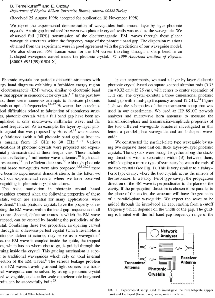
We tested this waveguiding agrument, by measuring the transmission properties of these structures along the plane of the cavity. Figure 2 shows the transmission properties of the waveguide structure for different separation widths. We ob-served full transmission ~100%! of the EM waves along a certain frequency range. The waveguiding was first observed at a minimum separation width around 10 mm, and the cutoff shifted to lower frequency values as the width of the air gap was increased. Independent of the width of the cavity, the guiding was observed to vanish at a fixed upper cutoff fre-quency ~13.2 GHz!, which corresponds to the upper band edge of the photonic band gap. This is along our expectations as the crystals do not act as mirrors~in all directions! beyond the full band gap frequencies. The lower cutoff frequency is determined by the width of the cavity and corresponds to the resonant frequency of the Fabry–Perot resonator. This reso-nant frequency can easily be predicted by a Fabry–Perot defect model we have used in our earlier work.24
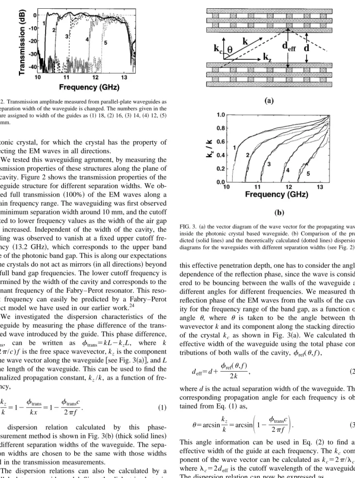
We investigated the dispersion characteristics of the waveguide by measuring the phase difference of the trans-mitted wave introduced by the guide. This phase difference,
ftrans, can be written as ftrans5kL2kzL, where k
5(2p/c) f is the free space wavevector, kzis the component
of the wave vector along the waveguide@see Fig. 3~a!#, and L is the length of the waveguide. This can be used to find the normalized propagation constant, kz/k, as a function of
fre-quency, kz k 512 ftrans kx 512 ftransc 2pf . ~1!
The dispersion relation calculated by this phase-measurement method is shown in Fig. 3~b! ~thick solid lines! for different separation widths of the waveguide. The sepa-ration widths are chosen to be the same with those widths used in the transmission measurements.
The dispersion relations can also be calculated by a parallel-plate waveguide model. Since the dielectric photonic crystal walls of the waveguide has a certain penetration depth that can be calculated using the reflection-phase infor-mation from the walls of the cavity, we can define an effec-tive width for the waveguide. This approach was previously used to investigate the defect characteristics built around di-electric and metallic photonic crystals.24In the calculation of
this effective penetration depth, one has to consider the angle dependence of the reflection phase, since the wave is consid-ered to be bouncing between the walls of the waveguide at different angles for different frequencies. We measured the reflection phase of the EM waves from the walls of the cav-ity for the frequency range of the band gap, as a function of angle u, where u is taken to be the angle between the wavevector k and its component along the stacking direction of the crystal kc as shown in Fig. 3~a!. We calculated the
effective width of the waveguide using the total phase con-tributions of both walls of the cavity,fref(u, f ),
deff5d1fref~u, f!
2k , ~2!
where d is the actual separation width of the waveguide. The corresponding propagation angle for each frequency is ob-tained from Eq.~1! as,
u5arcsinkkz5arcsin
S
12ftransc2pf
D
. ~3! This angle information can be used in Eq. ~2! to find an effective width of the guide at each frequency. The kccom-ponent of the wave vector can be calculated as kc52p/lc,
wherelc52deffis the cutoff wavelength of the waveguide. The dispersion relation can now be expressed as
kz
k 5
A
k22kc2
k . ~4!
Note that, since kc is considered to be constant, after some
frequency, the square root becomes real, so that the waves after that cutoff frequency ~defined by kc) can propagate in
FIG. 2. Transmission amplitude measured from parallel-plate waveguides as the separation width of the waveguide is changed. The numbers given in the plot are assigned to width of the guides as~1! 18, ~2! 16, ~3! 14, ~4! 12, ~5! 10.5 mm.
FIG. 3. ~a! the vector diagram of the wave vector for the propagating wave inside the photonic crystal based waveguide.~b! Comparison of the pre-dicted~solid lines! and the theoretically calculated ~dotted lines! dispersion diagrams for the waveguides with different separation widths~see Fig. 2!.
487
Appl. Phys. Lett., Vol. 74, No. 4, 25 January 1999 B. Temelkuran and E. Ozbay
the guide. For frequencies less than the cutoff frequency, kz
is imaginary, and such modes ~evanescent modes! cannot propagate in the waveguide.25 Figure 3~b! compares the parallel-plate waveguide model dispersion relations @ob-tained from Eq. ~5!, dotted lines# with the dispersion rela-tions obtained from the transmission phase measurements
@using Eq. ~1!, solid lines#. As can be seen from the plots, the
results are in good agreement for different separation widths of the guide, except for the higher frequency regions of the waveguide. This discrepancy is mainly related to the inaccu-rate reflection phase information ~due to experimental limi-tations! at higher incidence angles, u.70°.
As we have pointed earlier, photonic crystal based waveguides were predicted to have the property of guiding the wave through sharper bends.6To demonstrate this effect, we constructed an L-shaped waveguide in the following manner. We coupled the output of the previously described planar waveguide structure, to the input of an other but iden-tical waveguide making 90° with the first one, as shown in the second configuration of the setup~Fig. 1!. Each wall of the waveguide is a two unit cell photonic crystal. The width of the cavity is kept at a value of 2 cm, for which the fre-quency range of the waveguide will overlap with the full band gap of the crystals. Figure 4 shows the transmission of the EM waves through the L-shaped waveguide. The maxi-mum magnitude of the transmitted single was 35% of the incident signal. The frequency range of the L-shaped wave-guide again covers the full band gap frequencies of the pho-tonic crystal. As can be seen from Fig. 1, the L-shaped wave-guide is slightly asymmetric. We checked the effect of this asymmetry by interchanging the positions of the receiver and transmitter antennas, and measuring the transmission proper-ties of the waveguide. The resulting transmission character-istics of the waveguide were very similar to the original mea-surements. The relatively poor performance of the transmission magnitude can be further increased by a proper design of the bend. These results show that photonic crystals
can be used for various waveguide configurations.
In summary, we have experimentally verified that EM wave can be guided with 100% transmission, using three dimensional photonic crystals. We have developed a parallel-plate waveguide model for our structures. The dis-persion diagrams calculated using the transmitted phase mea-surements and by the waveguide model were in good agree-ment. We also observed 35% transmission for the EM waves traveling through a sharp bend in an L-shaped waveguide.
This work is supported by the Turkish Scientific and Technical Research Council of TURKEY~TU¨BI˙TAK! under Contract No. 197-E044, NATO Grant No. SfP971970, Na-tional Science Foundation Grant No. INT-9512812, and NATO-Collaborative Research Grant No. 950079.
1K. M. Ho, C. T. Chan, and C. M. Soukoulis, Phys. Rev. Lett. 65, 3152
~1990!.
2E. Yablonovitch, T. J. Gmitter, and K. M. Leung, Phys. Rev. Lett. 67,
2295~1991!.
3S. John, Phys. Rev. Lett. 58, 2486~1987!. 4
For a recent review, see articles in Photonic Band Gap Materials, edited by C. M. Soukoulis~Plenum, New York, 1996!.
5J. D. Joannopoulos, P. R. Villeneuve, and S. Fan, Nature~London! 386,
143~1997!.
6J. D. Joannopoulos, R. D. Meade, and J. N. Winn, Photonic Crystals
~University of Princeton Press, Princeton, NJ, 1995!.
7V. Kuzmiak and A. A. Maradudin, Phys. Rev. B 55, 7427~1997!. 8M. M. Sigalas, C. T. Chan, K. M. Ho, and C. M. Soukoulis, Phys. Rev. B
52, 11744~1995!.
9D. F. Sievenpiper, E. Yablonovitch, J. N. Winn, S. Fan, P. R. Villeneuve,
and J. D. Joannapoulos, Phys. Rev. Lett. 80, 2829~1998!.
10M. J. Bloemer and M. Scalora, Appl. Phys. Lett. 72, 1676~1998!. 11C. C. Cheng, R.-C. Tyan, A. Scherer, Y. Fainman, G. Witzgall, and E.
Yablonovitch, J. Vac. Sci. Technol. B 15, 2764~1997!.
12
J. C. Knight, T. A. Birsk, P. St. J. Russel, and D. M. Atkin, Opt. Lett. 21, 1547~1996!.
13K. M. Ho, C. T. Chan, C. M. Soukoulis, R. Biswas, and M. Sigalas, Solid
State Commun. 89, 413~1994!.
14E. Ozbay, J. Opt. Soc. Am. B 13, 1945~1996!. 15
M. C. Wanke, O. Lehmann, K. Muller, Q. Wen, and M. Stuke, Science
275, 1284~1997!.
16S. Noda~personal communication!.
17E. R. Brown and O. B. McMahon, Appl. Phys. Lett. 67, 2138~1996!. 18
E. R. Brown and O. B. McMahon, Appl. Phys. Lett. 68, 1300~1996!.
19
S.-Y. Lin, V. M. Hietala, S. K. Lyo, and A. Zaslavsky, Appl. Phys. Lett.
68, 3233~1996!.
20B. Temelkuran, E. Ozbay, J. P. Kavanaugh, and G. Tuttle, Appl. Phys.
Lett. 72, 2376~1998!.
21
J. G. Maloney, M. P. Kesler, B. L. Shirley, and G. S. Smith, Microwave Opt. Technol. Lett. 14, 261~1997!.
22T. F. Krauss, B. Vogele, C. R. Stanley, and R. M. De La Rue, IEEE
Photonics Technol. Lett. 9, 176~1997!.
23
A. Mekis, J. C. Chen, I. Kurland, S. Fan, P. R. Villeneuve, and J. D. Joannapoulos, Phys. Rev. Lett. 77, 3787~1996!.
24E. Ozbay and B. Temelkuran, Appl. Phys. Lett. 69, 743~1996!. 25J. D. Jackson, Classical Electrodynamics, 2nd ed. ~Wiley, New York,
1975!. FIG. 4. Transmission characteristics of the L-shaped waveguide.
488 Appl. Phys. Lett., Vol. 74, No. 4, 25 January 1999 B. Temelkuran and E. Ozbay