Optical properties of selenium sulfide thin film produced
via chemical dropping method
İ. Afşin Kariper1 · Şadan Özden2 · Fatma Meydaneri Tezel3
Received: 9 February 2018 / Accepted: 9 November 2018 / Published online: 14 November 2018 © Springer Science+Business Media, LLC, part of Springer Nature 2018
Abstract
This paper describes the production of selenium sulfide (SeS2) crystalline thin film on commercial glass substrates, via chemical bath deposition. Transmittance, absorption, die-lectric constant and refractive index of the produced films were investigated by UV/VIS Spectrum. It was found that changes occurred on the characteristics of the films and they were determined as a function of selenium sulfide concentration, which varied between 2 × 10⁻³ and 5 × 10⁻³ M. The structure of the film was analyzed using FTIR spectrum. The calculated refractive index values fell between 1.5 and 1.6, whereas the transmission ratio of the films was around 80–90%. Moreover, a peak in the reflectance was observed at 320–330 nm for all investigated samples. The highest dielectric constant for the films was obtained at the deposition concentration of 0.005 M. This study is believed to be useful for thin film production.
Keywords SeS2 thin films · Chemical dropping · Thin film · Selenium sulfide · Organic thin film
1 Introduction
Selenium and Sulfur are important elements for optical and photonic applications. Both elements are widely used in many areas, from solar batteries to photoelectric sensors, from laser printers to X-ray devices and from waveguides to lenses (Chaudhary and Mehta 2014; Mansour et al. 2018; Cui et al. 2013). However, studies on optical and electronic prop-erties of selenium and sulfide compound are limited in the literature (Khan et al. 2010;
This article is part of the Topical Collection on Optics in Materials, Energy and Related Technologies 2018.
Guest Edited by Yen-Hsun Su, Songnan Qu, Yiting Yu, Wei Zhang. * İ. Afşin Kariper
1 Education Faculty, Erciyes University, 38039 Kayseri, Turkey 2 Faculty of Science, Muğla Sıtkı Koçman University, Muğla, Turkey 3 Engineering Faculty, Karabük University, Karabük, Turkey
Premchander et al. 2004). A suitable manufacturing method of this compound will allow the production of photonic devices at low cost and high capacity compared to semiconduc-tor alternatives.
The production of selenium sulfide film from selenium cation and sulfide anion is very difficult. Selenium sulfide mixtures synthesized from selenium and sulfur give rise to numerous “alloys”. Thus, selenium sulfide film cannot be produced via chemical bath deposition. Selenium disulfide, which is referred as selenium sulfide, has a composition similar to SeS2. But, as used in proprietary formulations, it is not a pure chemical com-pound, it is a mixture with Se:S ratio = 1:2. Its components are cyclic Se–S rings con-taining a variable number of S and Se atoms, SenS8−n (Steudel and Laitinen 1982). There were several isomers depending on the relative placement of the selenium atoms in the ring: 1,2; 1,3; 1,4; 1,5 (Maaninen et al. 1999). Isomer 1,2 can be prepared by the reaction of chlorosulfanes and dichlorodiselane with potassium iodide in carbon disulfide (Laitinen et al. 1989). Many isomers of selenium sulfide are soluble in carbon disulfide, which cre-ated an advantage to be used in chemical dropping method.
The aim of this paper is describing the production of SenS8−n thin film via chemical dropping method and examining structural, optical and electrical properties of the pro-duced thin films. This type of thin film has not been propro-duced successfully up to now, thus there is no information about its structural, optical, and electrical properties.
2 Experimental
Selenium sulfide and carbon disulfide were procured as analytical pure material from Sigma Aldrich. Solutions containing different amount of selenium disulphide were pre-pared in carbon disulphide solvent. The concentrations of the solutions were 2 × 10⁻³ − 3 × 10⁻³ − 4 × 10⁻³ – 5 × 10⁻³ M. 20 ml of the solution was coated on glass substrates by dipping three times at room temperature (dip coating method). Then, all films were dried at room temperature. After 15 min, the carbon disulphide solvent on the films was evapo-rated and eventually selenium disulphide was deposited on the surface. The optical meas-urements of SenS8−n film were determined by Hach Lange DR 5000 Spectrophotometer at room temperature. An uncoated identical commercial glass substrate was placed in the ref-erence beam during the measurements. The optical spectrum of thin films was recorded in the wavelength range of 300–1100 nm at room temperature. The infrared spectrum of the SenS8−n was recorded by a Perkin Elmer Spectrum 400 spectrometer with a resolution of 4 cm−1 using a DTGS detector and 10 scans for each spectrum. The film thicknesses were measured with a Veeco Multi Mode AFM (Controller = NanoScope 3D). Thicknesses were measured in a 10 × 10 μm area with tapping mode.
3 Results and discussion
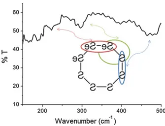
The vibrational spectrum of SeS thin film that is given in Fig. 1 was recorded by Perkin Elmer Spectrum 400 spectrometer (TGS detector).
• The S–S band (stretching) vibrations were observed at 464–488 cm−1. • The Se–Se band (stretching) vibrations were observed at 270–290 cm−1. • The Se–S stretching vibrations were observed at 371–387–390 cm−1.
These results are in line with the literature (Alparone 2012; Komulainen et al. 2002; Riv-ero et al. 2002). Eysel and Sunder (1979) showed that the vibration bands of SenSn-1 were in the range of 340–386 cm−1 for Se–S. Hendra and Park (1968) showed that S–S bonds were around 455 and 309 cm−1 and Se–Se bonds were 244–280 cm−1, approximately.
The transmittance (T) of sulfide thin film has been calculated by using reflectivity (R) and absorbance (A) spectra from the equation:
The transmittance (T) and reflectance (R) ratios are shown in Fig. 2 as a function of wave-length, for different concentrations. As expected, transmittance decreases as concentration increases. Transmittance ratio, which is in the range of 80–90% dramatically decreases to 60% for the sample with 0.004 M concentration. These results are similar for reflectance.
A characteristic reflectance spectrum peak occurred in the range of 320–330 nm for all the samples. The refractive index (n) and extinction coefficient (k) are calculated by using the following equations;
(1)
T =(1 − R2) e−A
Fig. 1 FTIR spectrum of SeS2 Thin Film
Fig. 2 Transmittance (T) and reflectivity (R) for selenium sulfide thin films at different concentrations 400 600 800 1000 50 60 70 80 90 100 0.002 M 0.003 M 0.004 M 0.005 M % T Wavelength (nm) 400 600 800 1000 4 8 12 16 % R Wavelength (nm) 60 50 I- 40 30 20 200 300 400 500 -1 Wavenumber ( cm ) • 0
"'
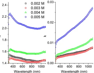
•As shown in Fig. 3, refractive index values obtained from the computations are around 1.5–1.6.
As the concentration increases, n values raise for the first three samples and rapidly hits 2 for the sample with 0.005 M concentration; whereas k values vary linearly with the wavelength and for the sample with 0.005 M density, the slope of this linear change is larger than others.
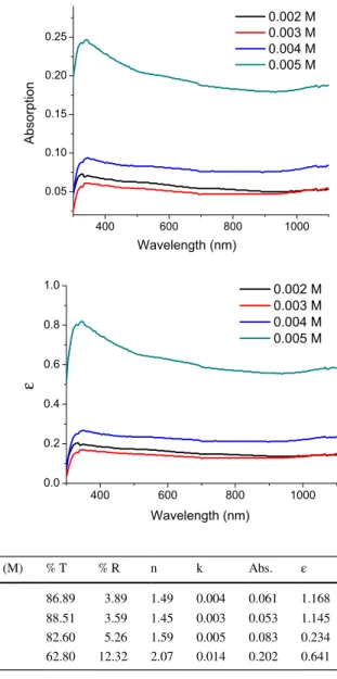
Figure 4 shows absorbance and dielectric constant of selenium sulfide thin films as a function of concentration. The absorption values are found to be in the range of 0.05–0.01 for the samples with low concentration, but it reaches 0.20–0.25 for the film with 0.005 M concentration. A similar wavelength-dependent behavior is also observed for dielectric constant. The material that we measure should not have any magnetic fea-ture, since n = √µ.ε. Usually, it is assumed that the materials with µ = 1 lack magnetic properties and the equation of refractive index is derived.
In addition, all these parameters are calculated in the visible region (550 nm) as a function of concentration and the results are summarized in Table 1. In terms of vis-ible light applications, the prepared SeS2 films displayed high transmittance and low reflectance up to the 0.004 M concentration. These parameters obviously change for the samples with larger concentration than the density mentioned above. The refrac-tive index (n) values are around 1.5 and k values are in the range of 0.003–0.005 for first three samples, with low concentration. However, for the sample with 0.005 M con-centration, n exceeds 2 and k increases rapidly. Greater unity dielectric constant values are obtained for the samples with 0.001 M and 0.002 M concentration, in this visible region. An organic thin film material having these properties can be used as a detector in the far IR region with its high transmittance (Negas et al. 1992) and it is useful for Fresnel lens application because of its low transmittance in the UV region (Xi et al.
2007). Additionally, dielectric constant value of the film is quite low, which makes it useful in wide areas of material applications owing to containing small cracks in the (2) n = (1 + R) (1 − R)+ √ 4R (1 − R2)− k 2 k = 𝛼𝜆 4n
Fig. 3 The refractive index (n) and the extinction coefficient (k) for selenium sulfide thin films at different concentrations 400 600 800 1000 1.4 1.6 1.8 2.0 2.2 2.4 0.002 M 0.003 M 0.004 M 0.005 M n Wavelength (nm) 400 600 800 1000 0.00 0.01 0.02 0.03 k Wavelength (nm) • 0
structure, no exposing to metal corrosion and having low thermal coefficient (Xi et al.
2007; Volksen et al. 2010).
As can be seen from Fig. 5, film thickness increases as the chemical spent increases (except 0.003 molar bath concentration), which is expected from chemical bath method. Film thickness varied between 85 mm and up to 450 mm, which is reflected on the opti-cal parameters as well. With the increase of film thickness, % T optiopti-cal transparency decreases, whereas refraction index, absorption and dielectric constant increase. Similar results have been underlined by Kariper (2015, 2016), who has revealed that optical transparency decreases and absorption and refraction index increase with the increase of film thickness.
Fig. 4 The optical absorbance and the dielectric constant values of selenium sulfide at different concentrations 400 600 800 1000 0.05 0.10 0.15 0.20 0.25 Absorption Wavelength (nm) 0.002 M 0.003 M 0.004 M 0.005 M 400 600 800 1000 0.0 0.2 0.4 0.6 0.8 1.0 Wavelength (nm) 0.002 M 0.003 M 0.004 M 0.005 M ε
Table 1 The optical values in the visible region (550 nm) as function concentration Conc. (M) % T % R n k Abs. ε 0.002 86.89 3.89 1.49 0.004 0.061 1.168 0.003 88.51 3.59 1.45 0.003 0.053 1.145 0.004 82.60 5.26 1.59 0.005 0.083 0.234 0.005 62.80 12.32 2.07 0.014 0.202 0.641
According to these results, selenium disulfide can be used for developing mid-infrared photonics integrated circuits like as silicon and germanium (Cheng et al. 2012; Xiao et al.
2018). As we can see in the Fig. 1, selenium disulfide can be used as ring resonator down to 200–300 cm−1 wavelength. And also, it can be used filter up to 500 cm−1 wavelength.
4 Conclusion
Selenium sulfide (SeS2) crystalline thin films were produced via chemical bath deposition on commercial glass substrates. By changing the concentration of SeS2, four different thin films were produced and their optical properties were examined. Up to 0.004 M concen-tration, thin films displayed high optical transmittance and had low reflectivity. When the concentration of the solution exceeded 0.005 M, these optical values changed dramatically. Similar concentration-dependent behavior was also observed for n, k, ε values and absorb-ance. These parameters were examined in detail within the visible region. For the sam-ples with 0.002 M and 0.003 M concentration, dielectric constant values were found to be greater than unity and high transmittance properties were observed for samples with a concentration 0.003 M and below. SeS2 thin films deposited in lower concentration can be produced easily via chemical bath and can be used as a transparent layer for different opti-cal applications.
References
Alparone, A.: Density functional theory Raman spectra of cyclic selenium clusters Sen (n = 5–12). Comput. Theor. Chem. 988, 81–85 (2012)
Chaudhary, S., Mehta, S.K.: Selenium nanomaterials: applications in electronics, catalysis and sensors. J. Nanosci. Nanotechnol. 14(2), 1658–1674 (2014)
Cheng, Z., Chen, X., Wong, C.Y., Xu, K., Tsang, H.K.: Mid-Infrared suspended membrane waveguide and ring resonator on silicon-on-insulator. IEEE Photonics 4, 1510–1519 (2012)
Cui, S., Chahal, R., Boussard-Plédel, C., Nazabal, V., Doualan, J.-L., Troles, J., Bureau, B.: From selenium- to tellurium-based glass optical fibers for infrared spectroscopies. Molecules 18(5), 5373–5388 (2013)
0,002 0,003 0,004 0,005 100 200 300 400 500 d (nm) Bath Concentration Fig. 5 Film thickness according to bath concentration
Eysel, H.H., Sunder, S.: Homonuclear bonds in sulfur-selenium mixed crystals: a Raman spectroscopic study. Inorg. Chem. 18, 2626–2627 (1979)
Hendra, P.J., Park, P.J.D.: The vibrational spectra of sulphur and selenium Monohalides. J. Chem. Soc. A (1968). https ://doi.org/10.1039/J1968 00009 08
Kariper, İ.A.: Optical and structural properties of zinc iodine thin films. Opt. Mater. 44, 78–83 (2015) Kariper, İ.A.: Structural, optical and porosity properties of CdI2 thin film. J. Mater. Res. Technol. 5, 77–83
(2016)
Khan, M.A.M., Khan, M.W., Alhoshan, M., AlSalhi, M.S., Aldwayyan, A.S., Zulfequar, M.: Structural, optical and electrical characterization of selenium sulphide nanostructured thin film. Mater. Lett.
64(17), 1929–1932 (2010)
Komulainen, J., Laitinen, R.S., Suontamo, R.J.: A theoretical study of the 77Se NMR and vibrational spec-troscopic properties of SenS8n ring molecules. Canad. J. Chem. 80, 1435–1443 (2002)
Laitinen, R.S., Pekonen, P., Hiltunen, Y., Pakkanen, T.A.: The 77Se NMR spectroscopic identification of heterocyclic selenium sulfides prepared by the reactions of chlorosulfanes and dichlorodiselane with potassium iodide. Acta Chem. Scand. 43, 436–440 (1989)
Maaninen, A., Chivers, T., Parvez, M., Pietikäinen, J., Laitinen, R.S.: Syntheses of THF solutions of SeX2(X = Cl, Br) and a new route to selenium sulfides SenS8−n (n = 1 − 5): X-ray crystal structures of SeCl2(tht)2 and SeCl2·tmtu. Inorg. Chem. 38, 4093–4097 (1999)
Mansour, B.A., Zawawi, I.K.E.L., Elsayed-Ali, H.E., Hameed, T.A.: Preparation and characterization of optical and electrical properties of copper selenide sulfide polycrystalline thin films. J. Alloy. Compd.
740, 1125–1132 (2018)
Negas, T., Yeager, G., Bell, S., Coates, N., Minis, I.: BaTi4O9/Ba2Ti9O20—based ceramics resurrected for modern microwave applications. Am. Ceram. Soc. Bull. 72, 80–89 (1992)
Premchander, P., Arivuoli, D., Baskar, K.: Investigations of structural and optical analysis of SeS and SeSnS2 microcrystals. J. Cryst. Growth 267(1–2), 166–172 (2004)
Rivero, C., Schulte, A., Richardson, K.: Structure-property relationships in As–S–Se glasses for waveguide applications probed by waveguide Raman spectroscopy. Ceram. Trans. 126, 79–85 (2002)
Steudel, R., Laitinen, R.S.: Cyclic selenium sulfides. Top. Curr. Chem. 102, 177–197 (1982)
Volksen, W., Miller, R.D., Dubois, G.: Low dielectric constant materials. Chem. Rev. 110, 56–110 (2010) Xi, J.Q., Schubert, M.F., Kim, J.K., Schubert, E.F., Chen, M., Lin, S.Y., Liu, W., Smart, J.A.: Optical thin
film materials with low refractive index for broadband elimination of Fresnel reflection. Nat. Photonics
1, 176–179 (2007)
Xiao, T.H., Zhao, Z., Zhou, W., Chang, C.Y., Set, S.Y., Takenaka, M., Tsang, H.K., Cheng, Z., Goda, K.: Mid-infrared high-Q germanium microring resonator. Optic Let. 43, 2885–2888 (2018)