COLLOIDAL PHOTONICS OF
SEMICONDUCTOR NANOCRYSTALS:
FROM POLARIZED COLOR CONVERSION
TO EFFICIENT SOLAR CONCENTRATION
a dissertation submitted to
the graduate school of engineering and science
of bilkent university
in partial fulfillment of the requirements for
the degree of
doctor of philosophy
in
electrical and electronics engineering
By
Kıvan¸c G¨
ung¨
or
July 2018
COLLOIDAL PHOTONICS OF SEMICONDUCTOR NANOCRYS-TALS: FROM POLARIZED COLOR CONVERSION TO EFFI-CIENT SOLAR CONCENTRATION
By Kıvan¸c G¨ung¨or July 2018
We certify that we have read this dissertation and that in our opinion it is fully adequate, in scope and in quality, as a dissertation for the degree of Doctor of Philosophy.
Hilmi Volkan Demir(Advisor)
Fatih ¨Omer ˙Ilday
Mehmet Selim Hanay
Sefer Bora Li¸sesivdin
Emre Sarı
ABSTRACT
COLLOIDAL PHOTONICS OF SEMICONDUCTOR
NANOCRYSTALS: FROM POLARIZED COLOR
CONVERSION TO EFFICIENT SOLAR
CONCENTRATION
Kıvan¸c G¨ung¨or
Ph.D. in Electrical and Electronics Engineering Advisor: Hilmi Volkan Demir
July 2018
Effective photon management is pivotal to the success of future photonic applica-tions. The demand for high-performance electronic displays and solar light har-vesters has been increasingly growing, ever with high expectations in advancing their power efficiencies. Semiconductor nanocrystals are highly promising for use in such advanced photonic applications. However, conventional device architec-tures and fabrication methods cannot fully exploit their potential. To address the need for their effective utilization, in this thesis, we proposed and demonstrated novel photon managing methods for colloidal nanocrystals to target polarized color conversion and efficient solar concentration. Nanocrystals possess an un-matched color purity for next-generation displays but color enrichment in displays suffers from the inherent random polarization in their photoluminescence. Instead of clipping the undesired polarization, we show a new class of v-shaped backlight unit (v-BLU) creating Fano resonances to enforce isotropic quantum emitters of the integrated color-conversion nanocrystals to emit polarized light. While en-abling a front-panel configuration, the proposed v-BLU of nanocrystals allows for a strong modification of the density of optical states via resonance coupling. This control over the density of states for isotropic quantum dots empowers the realization of high polarization contrast ratios while sustaining their optical trans-mission. Similar to color conversion, colloidal nanocrystals are also instrumental to light harvesting, in particular using atomically flat nanocrystals with their step-like absorption profile making them potentially ideal candidates for lumi-nescent solar concentrators (LSCs). Nevertheless, practically zero Stokes shift in their photoluminescence fundamentally limits their utilization. Here we overcame this limitation by proposing the doping of such colloidal quantum wells inducing a large Stokes shift with near-unity photoluminescence quantum efficiency. We
iv
quantum wells outperforming the LSCs of their undoped counterparts and doped quantum dots. The LSCs of such Cu-doped quantum wells offer record optical flux gain compared to other colloids. We believe that the findings presented in this thesis will advance the applications of colloidal nanocrystals boosting the performance of their next-generation photonic devices to unprecedented levels.
¨
OZET
YARI˙ILETKEN NANOKR˙ISTALLER˙IN KOLO˙IDAL
FOTON˙I ˘
G˙I: POLAR˙IZE RENK D ¨
ON ¨
US
¸ ¨
UM ¨
UNDEN
VER˙IML˙I G ¨
UNES
¸ IS
¸I ˘
GI YO ˘
GUNLAS
¸TIRILMASINA
Kıvan¸c G¨ung¨or
Elektrik ve Elekronik M¨uhendisli˘gi, Doktora Tez Danı¸smanı: Hilmi Volkan Demir
Temmuz 2018
Etkili foton y¨onetimi gelecekteki fotonik uygulamaların ba¸sarısı i¸cin ¸cok ¨
onemlidir. Y¨uksek performanslı elektronik ekranlar ve g¨une¸s ı¸sı˘gı toplayıcılarına y¨onelik talep, ¨ozellikle g¨u¸c verimlili˘gini artırmaya y¨onelik y¨uksek beklentilerle, birlikte giderek artmaktadır. Yarı iletken nanokristaller, bu t¨ur geli¸smi¸s fo-tonik uygulamalarda kullanım i¸cin olduk¸ca ¨umit vericidir. Ancak, geleneksel cihaz mimarileri ve ¨uretim y¨ontemleri bu nanokristallerin potansiyellerini tam olarak kullanamamaktadır. Etkili kullanım gereksinimini kar¸sılamak ama¸clı, bu tezde polarize renk d¨on¨u¸s¨um¨u ve verimli g¨une¸s konsantrasyonunu hede-fleyen koloidal nanokristaller i¸cin yeni foton y¨onetme y¨ontemlerini ¨onerdik ve g¨osterdik. Nanokristaller, yeni nesil ekranlar i¸cin e¸ssiz bir renk saflı˘gına sahip olmakla birlikte, g¨or¨unt¨ulerdeki renk zenginli˘gi, kuantum noktacıkların rasgele polarizasyona sahip fotol¨uminesansından muzdariptir. ˙Istenmeyen polarizasyonu kesmek yerine, t¨umle¸sik renk d¨on¨u¸st¨ur¨uc¨u nanokristallerin izotropik kuantum yayıcılarını polarize ı¸sık yaymaya zorlayan, Fano rezonansları yaratan yeni bir sınıf v-¸sekilli arka ı¸sık birimi (v-BLU) g¨osterdik. On panel konfig¨¨ urasyonuna imkan verirken, ¨onerilen v-BLU nanokristalleri, rezonans e¸sle¸smesi yoluyla op-tik durum yo˘gunlu˘gunun kuvvetli bir modifikasyonunu m¨umk¨un kılmaktadır. ˙Izotropik kuantum noktacıklarının durum yo˘gunlu˘gu ¨uzerindeki bu kontrol, optik iletimlerini s¨urd¨ur¨urken y¨uksek polarizasyon kontrast oranlarının elde edilmesini sa˘glar. Renk d¨on¨u¸s¨um¨une benzer ¸sekilde, koloidal nanokristaller ı¸sıyan g¨une¸s ı¸sı˘gı yo˘gunla¸stırıcılarında (LSC’ler) kullanım i¸cin olduk¸ca etkilidir. ¨Ozellikle basamak benzeri so˘gurma profiline sahip atomik olarak d¨uz nanokristaller, LSC’ler i¸cin potansiyel olarak ideal adaylardır. Bununla beraber, fotol¨uminesanslarında pratikte sıfır olan Stokes kaymaları, kullanımlarını sınırlandırmaktadır. Bu sınırlamanın, %100’e yakın bir fotol¨uminesans kuantum verimlili˘gi ile b¨uy¨uk bir
vi
¨
ustesinden geldik. Geli¸stirdi˘gimiz bakır katkılı kuantum kuyucuklarından yapılan LSC panellerinin, katkısız muadillerinin ve katkılı kuantum noktacıklarının LSC’lerinden daha y¨uksek performanslı oldu˘gunu g¨osterdik. Bu t¨ur bakır katkılı kuantum kuyucuklarının LSC’leri, di˘ger koloidlere kıyasla rekor d¨uzeyde optik akı kazancı sunmaktadır. Bu tezde sunulan bulguların, yeni nesil fotonik cihazların performansını daha ¨once g¨or¨ulmemi¸s seviyelere ta¸sıyacak koloidal nanokristallerin uygulamalarını ilerletece˘gine ve geli¸stirece˘gine inanıyoruz.
Acknowledgement
First, I would like to thank my advisor Prof. Hilmi Volkan Demir. It was 2008 summer when I first met with Prof. Demir trying to introduce myself as a fellow Ankara Science High School graduate and I was impressed with his passion and excitement about his research. Looking back after ten years, I can clearly say that it was a life-changing moment for me. I was enthusiastic to achieve greater things and lucky to have a mentor like him who has been a great role model and visionary scientist. I hope that I have learned a lot from him and I would like to express my sincere gratitude to him for his positive attitude.
I would like to thank my thesis monitoring committee members Prof. Fatih ¨
Omer ˙Ilday, Asst. Prof. Selim Hanay and Prof. Ayhan Altınta¸s for their support and valuable discussions. I would like to sincerely thank my jury members Prof. Sefer Bora Li¸sesivdin and Asst. Prof. Emre Sarı for serving in my Ph.D. jury and for their comments and suggestions. I would like to also thank Prof. Orhan Aytur, Prof. D¨on¨u¸s Tuncel and Prof. ¨Ozay Oral for their support during my Ph.D. and Prof. Sergey V. Gaponenko and Asst. Prof. Sedat Nizamo˘glu for their support during my postdoctoral position applications.
I would like to acknowledge and thank TUB˙ITAK-B˙IDEB for the financial support throughout this thesis.
Ph.D. is a team work and I had the best team; I would like to thank my broth-ers and sistbroth-ers from Office 306: Emre ¨Unal, ¨Ozg¨un Aky¨uz, Dr. Yusuf Kele¸stemur, Dr. Burak G¨uzelt¨urk, Dr. Can Uran, Dr. Talha Erdem, Dr. Zeliha Soran Erdem, Dr. Aydan Yeltik, Onur Erdem and Dr. Murat Oluta¸s for all the fun and friend-ship. My deepest gratitude goes to Dr. Manoj Sharma who has been a friend and mentor to me. I also thank past and present Demir Group members: Dr. Sedat Nizamo˘glu, Dr. Evren Mutlug¨un, Dr. Emre Sarı, Dr. Rohat Melik, Dr. Ahmet Fatih Cihan, Dr. Urartu ¨Ozg¨ur S¸afak S¸eker, Dr. Nihan Kosku Perkg¨oz, Dr. Pedro Ludwig Hernandez-Martinez, Dr. Vijay Kumar Sharma, Ashma Sharma, Dr. Sava¸s Delikanlı, Dr. Tuncay ¨Ozel, Dr. ˙Ilkem ¨Ozge ¨Ozel, Dr. Akbar Alipour, Berkay Bozok, Halil Akcalı, ˙Ibrahim Akcalı, C¨uneyt Ero˘glu, Dr. Onur Akın, Dr. Mustafa Akın Sef¨un¸c, Yasemin Co¸skun, Dr. Sayım G¨okyar, Dr. Veli Tayfun
viii
Yerli, Didem Dede, Shahab Akhavan, Nima Taghipour, Togay Amirahmadov, Can Fırat Usanmaz, Dr. Negar Gheshlaghi, Dr. Volodymyr Sheremet, Dr. Yem-liha Altınta¸s, Muhammad Hamza Humayun, Selim Bozdo˘gan, Farzan Shabani, Ulviyya Quliyeva, Mustafa Sak and ˙Ibrahim Tanrı¨over. I strongly believe that Dr./non-Dr. ratio in this list will tremendously increase in the near future. Also, Birsen Bilgili deserves a special thank for taking care of us and delicious organi-zations.
I thank all the technical and administrative staff at UNAM, Advanced Re-search Labs and EEE Department, especially M¨ur¨uvet Parlakay, Duygu Kazancı, Ay¸seg¨ul Torun, Mustafa Do˘gan, Mustafa G¨uler and Murat G¨ure, who made ev-erything easier.
There is no way I can truly express my gratitude to my parents -Aynur and Mehmet- and my brother ˙Inan¸c. I have the best family one can imagine, and their support is invaluable. I am fortunate to have a brother that knows and understands me better than anyone else, I hope that our fun never ceases.
Finally, my special thanks go to my lovely wife, Yasemin. I also would like to thank my family-in-law for their support and sharing Yasemin with me. She is the joy and color of my world. In my M.S. thesis, I had written “I miss our undergraduate years a lot, yet too excited to see forthcoming years.”, now, after all these years, I am more excited than ever. Together with her, we are the best team and our journey just began.
Contents
1 Introduction ... 1
1.1 Organization of the thesis ...4
2 Basics... 6
2.1 Semiconductors ...7
2.2 Understanding Quantum Effects ... 11
2.3 Density of States for Electrons and Holes ... 14
2.4 Colloidal Semiconductor Nanocrystals ... 20
2.5 Plasmonics: Colorful Metals of Nanoworld ... 26
3 Fabrication and Characterization Techniques ... 35
3.1 Additive Methods ... 35
3.1.1 Thermal Deposition ... 36
3.1.2 Electron Beam Deposition ... 37
3.2 Etching Methods ... 38
3.2.1 Wet Etching ... 39
3.2.2 Dry Etching ... 42
3.3 Patterning Methods ... 45
3.3.1 Electron Beam Lithography (EBL) ... 46
3.3.2 Focused Ion Beam (FIB) Lithography ... 47
3.3.3 Template Stripping ... 49
3.4 Imaging Methods ... 51
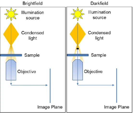
3.4.1 Brightfield and Darkfield Optical Microscopy ... 52
3.4.2 Back Focal Plane Imaging ... 54
3.4.3 Electron Microscopies ... 59
3.5.1 Absorption and Photoluminescence Spectroscopies ... 62
3.5.2 Absolute Quantum Efficiency Measurement ... 65
4 Polarized Color Conversion of Colloidal Nanocrystals Coupled to Plasmonic Surfaces ... 70
4.1 Motivation and Review ... 71
4.2 Working Principle ... 74
4.3 Fabrication of v-BLU Structure ... 77
4.4 Plasmonic Characterization of v-Grooved Surface ... 79
4.4.1 Optical Transmission Spectral Characterization of v-BLU ... 79
4.4.2 Numerical Simulations and Fano Resonance Line-shape ... 83
4.5 Photoluminescence Characterization of Coupled QDs ... 85
4.5.1 Steady-State Polarization Dependent Photoluminescence Measurements ... 85
4.5.2 Emission Kinetics Analysis of Plasmonically Coupled Quantum Dots ... 89
4.5.3 Dipole Orientation of Quantum Dots when Coupled to Plasmonic Surface 92 4.6 Proof-of-Concept LCD Application using v-BLU Backlighting ... 94
4.7 Summary ... 97
5 Luminescent Solar Concentration of Colloidal Nanocrystals ... 99
5.1 Motivation and Review ... 100
5.2 Structural and Optical Characterization of Cu-doped Nanoplatelets ... 104
5.3 Reabsorption Characterization of Cu-doped Nanoplatelets ... 117
5.4 Flux Gain Prediction of Cu-doped Nanoplatelets ... 127
5.5 Fabrication and Optical Characterization of Luminescent Solar Concentrators of Cu-doped Nanoplatelets ... 129
5.6 Optical Efficiency Characterization of Fabricated Nanoplatelet Luminescent Solar Concentrators ... 132
5.7 Summary ... 137
6 Conclusions and Future Outlook ... 138
6.1 General Conclusions ... 138
6.2 Outlook ... 140
6.3 Contributions of This Thesis to the Literature ... 142
List of Figures
Figure 2.1 Illustration of the band filling for different types of materials. ...9 Figure 2.2 A more realistic band structure of a direct bandgap semiconductor. ... 10 Figure 2.3 Illustration of infinite (left) and finite (right) square potential well problems for a particle with mass. ... 14 Figure 2.4 Different dimensionalities and their corresponding density of states illustrated from bulk to 0D. ... 19 Figure 2.5 The product of Fermi distribution and the density of states determines the absorption profile. The product of (1 − 𝑓(𝐸)) and the three-dimensional density of states (𝑔3𝐷(𝐸)) at 𝑇2 > 0 K successfully illustrates a typical absorption tail of a semiconductor. ... 20 Figure 2.6 Effect of quantum confinement on bulk semiconductor energy band diagram given in Figure 2.2. Quantization restricts only certain k values on the band diagram. 21 Figure 2.7 Bandgaps and relative band alignments of commonly used semiconductors for colloidal nanocrystals. After [27] © IOP Publishing. Reproduced with permission. All rights reserved. ... 24 Figure 2.8 Illustration of different types of the band alignments and their corresponding electron and hole wavefunction across the heterostructures of each nanocrystal. ... 25 Figure 2.9 Various 4 ML Type I and Type II CQWs under ambient lighting (top) and UV illumination (bottom) showing bright colors all across the visible spectrum from green to red (Demir Group). ... 25 Figure 2.10 The first known example of a plasmonic application: Lycurgus Cup. Dichroic behavior of the glass is originated from the incorporated metallic nanoparticles. © Trustees of the British Museum [29]. ... 27
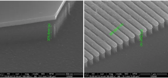
Figure 2.11 Kretschmann prism configuration for creating of SPPs (left) and the dispersion curve illustration (right) for the excitation mechanism. ... 30 Figure 3.1 Thermal deposition technique illustration. Evaporation material is heated inside a high critical-temperature evaporation boat under ultrahigh vacuum. A beam of material vapor is deposited uniformly on the substrate while the deposition thickness is tracked via a thickness monitor. ... 37 Figure 3.2 Electron beam deposition technique illustration. Inside a crucible, evaporation material is heated with a high current electron beam under ultrahigh vacuum. A beam of material vapor is deposited uniformly on the substrate while the thickness is tracked with a thickness monitor. ... 38 Figure 3.3 Si (100) surfaces imaged following different KOH etch recipes under the same contrast, brightness and magnification. ... 41 Figure 3.4 Anisotropic etching of Si (100) surface before (left) and after (right) Cr mask removal. ... 42 Figure 3.5 Anisotropic dry etching of silicon surface. While conventional Bosch process leaves nanometric trenches (left), the modified Bosch process leaves a smooth vertical profile (right)... 44 Figure 3.6 Modified Bosch process applied to silicon oxide (left) and chromium (right) etch masks on silicon surface. ... 44 Figure 3.7 a) Fabricated checkerboard structure with sharp corners. b) Monodisperse gold blocks with nanometer sized features. c) 50% duty cycle grating structure with a periodicity of 100 nm. ... 47 Figure 3.8 a) Gold bullseye structure with very thin lines. b) Nickel nanowire slicing for nanodisc fabrication. c) FIB milling for cross-sectional imaging of anisotropically etched Si masked by gold. ... 48 Figure 3.9 Silanization process illustration on a hot plate. ... 50 Figure 3.10 Results of our development of the template stripping from silicon surface having micrometer sized features. 300 nm silicon oxide masked surface of silicon is etched using anisotropic dry etching and silanized. A deposited thin layer of gold is peeled off the template using a supporting polymer layer. ... 50 Figure 3.11 Results of our additional examples of the template stripping from silicon surface. This time a thin chromium layer is used to mask the surface of silicon during anisotropic dry etching. After silanization, deposited thin layer of gold is peeled off the template with a supporting polymer layer. The wavy surface observed in some small structures is due to the supporting polymer swelling due to heating under the bombardment of the electron beam during SEM imaging. ... 51
Figure 3.12 Brightfield and darkfield microscopy configurations for the inverted optical microscope. ... 53 Figure 3.13 BFP pattern formation of aligned dipoles. When a polarizer is placed at the collection end, the modified polarization state of the light can be identified according to the propagation direction... 57 Figure 3.14 BFP imaging configuration. Depending on the application, a luminescent sample can be excited and a lens (called Bertrand lens) placed at one focal length behind the image plane images the BFP at one focal length behind the lens. ... 58 Figure 3.15 Our BFP imaging setup used to measure the dipole orientations of our emitters. A laser beam excites our nanocrystals from the top and a microscope objective collects the emitted light. Using a Bertrand lens the BFP is imaged on CCD. ... 58 Figure 3.16 Interaction mechanisms illustrated for a highly energetic electron beam interacting with material. Different interaction mechanisms are used for different analysis methods. (SEM: scanning electron microscopy, TEM: transmission electron microscopy, HR-TEM: high-resolution TEM, EDX: energy dispersive X-ray scattering, CL: cathodoluminescence, EELS; electron energy loss spectroscopy)... 61 Figure 3.17 Absorption spectroscopy. Generally, a broadband excitation source is used. However, to avoid errors with the excitation, the collection wavelength should be the same as the excitation and, if any, emission wavelength should be rejected. ... 63 Figure 3.18 Emission spectroscopy. A fluorophore is excited via a selected wavelength band of a broadband source. During this fixed excitation, the PL spectrum is scanned. ... 64 Figure 3.19 Photoluminescence excitation (PLE) spectroscopy. In contrast to PL spectroscopy, here the fluorophore emission wavelength is fixed. With the emission collected at this fixed wavelength, the excitation wavelength is scanned, and the PL intensity is recorded for tuned excitation wavelength. ... 65 Figure 3.20 Three configurations of the absolute PL QE: the blank, sample and scattering measurements are illustrated. ... 68 Figure 3.21 Exemplary spectra for the absolute PL QE calculation. Blank, sample and scattering spectra are shown with the excitation and emission portions. ... 69 Figure 4.1 Working principle of the v-grooved surface utilizing SPCE for highly polarized light generation at surface normal direction... 75 Figure 4.2 Proposed display architecture of v-BLU surface. Randomly polarized blue LED in surface normal configuration excites isotropic QDs on the v-BLU surface, however, emitted light from the QDs integrated intimately with the v-BLU is strongly linearly polarized towards liquid crystal cells. Inset figure illustrates excitation configuration of proposed v-BLU design. ... 76
Figure 4.3 Fabrication steps for mold with v-grooved surface features are shown. Starting with the pattern definition using EBL and consecutive Cr deposition and liftoff serves as protective layer for anisotropic dry etching step. After highly anisotropic silicon dry etch using ICP-RIE, modified anisotropic KOH wet etch of silicon defines the v-groove features on silicon surface. Finally, characteristic 54.7° angle is observed under cross-sectional imaging. ... 78 Figure 4.4 (a) Illustration of the developed fabrication method and final structure of the proposed v-BLU. After metal layer deposition, v-BLU together with support layer polymer is stripped off from silicon mold. (b) Cross-sectional SEM image of the fabricated mold structure. (c) Cross-sectional image of the replicated gold v-BLU with QDs. ... 79 Figure 4.5 (a) Transmission spectra of gold v-BLUs having different red QD layer thicknesses. Thicker QD layer results in red-shifted and increased transmission response for TM polarization. TE polarization for thin QD layered structures is similar to flat gold film transmission response plotted in gray shaded curve. (b) Transmission TM/TE ratio for gold v-BLU shows an increased polarization performance for structures with QDs. Around red QD emission peak wavelength (620 nm) TM/TE ratio is ~5 for both structures. Gray shaded curve of flat gold film TM/TE ratio is unity as expected. ... 81 Figure 4.6 (a) Transmission spectra of silver v-BLU before and after green QD layer deposition. Presence of QD layer results in red-shifted and increased transmission response for TM mode similar to gold v-BLU. (b) Transmission TM/TE ratio for silver v-BLU shows an increased polarization performance after QDs deposition. Around green QD emission peak wavelength (540 nm) TM/TE ratio is ~7. ... 82 Figure 4.7 (a) Experimental and simulated transmission spectra of gold v-BLU. (b) Experimental and simulated transmission spectra of silver v-BLU. ... 82 Figure 4.8 FDTD modeling of gold v-BLU without a QD layer. TM and TE polarization orientations are illustrated on the left and when deposited on v-BLU, the position of QDs are shown in red color. TM polarization transmission response resembles Fano type resonance line shape and observed higher transmission for higher energies is an indication for forward scattering configuration. Electric field intensity maps are showing increased transmission for the lower wavelengths than resonance wavelength of 615 nm. Also, the gap where QDs are deposited shows an increased electric field intensity, which increases the optical density of states for QDs. TE polarization shows no sign of strong resonance behavior and both transmission and electric field density values are significantly lower than TM polarization. ... 84 Figure 4.9 Farfield polarization dependent PL intensity measurement setup. Similar to LCD operation mechanism, emitted light of isotropic QDs coupled to v-BLU passes through an analyzer and a color filter to cancel out laser light. Using a spectrometer, we measure the intensity spectrum of the under different angles of the analyzer. Laser excitation polarization is 45° to the groove directions ensuring equal excitation of both TM and TE polarizations. ... 86
Figure 4.10 Absorption and emission spectra of red (λPL = 620 nm) and green (λPL = 540 nm) QDs used in this study are shown with corresponding TM polarization transmission spectra of gold and silver v-BLUs. ... 87 Figure 4.11 Analyzer angle dependent PL intensity for red QDs follows a well-defined cos2 dependence with CR=9.70. Gray spheres are PL intensity of QDs on flat gold film
and the absence of cos2 dependence is an indicator for the absence of measurement
system related anisotropy. ... 87 Figure 4.12 Analyzer angle dependent PL intensity for green QDs follows a well-defined cos2 dependence with CR=4.32. ... 88
Figure 4.13 Maximum and minimum PL spectra of red and green QDs in TM and TE polarizations showing high CR and no significant peak wavelength change... 88 Figure 4.14 Conventional in solution anisotropy measurement configuration using time resolved fluorescence measurement setup. In vertical polarization excitation, only vertical dipole is created and allows to measure the anisotropy in this configuration. To eliminate the system related anisotropies G factor calculation is required. Created dipole in horizontal configuration is isotropic with respect to the collection end and any measured anisotropy must be system related... 90 Figure 4.15 Our proposed anisotropy measurement configuration for in-film measurements. 45° placed groove orientation of the sample ensures the excitation both polarization states. G factor is calculated from nonpatterned QD film which would give 0 anisotropy inherently. TM and TE polarization measurements are corrected according to this measured G factor. ... 91 Figure 4.16 Time resolved fluorescence analysis of red QD films shows a strong modification in density of optical states for QDs. While average lifetime of plain QD film is 10.08 ns, decay rate increases when QDs are in a proximity of gold layer (for QDs on plain gold layer 𝜏𝑎𝑣 = 0.70 ns). Increased PL intensity and the fastest decay (𝜏𝑎𝑣 = 0.39 ns) observed in TM polarization PL of QDs indicate a pronounced anisotropy which is measured as 0.76 from transient analysis agreeing well with steady-state measurements. Inset figure zooms into the initial times of the decay curves and shows similar transient response for TE polarization and plain gold film emissions. Gray curve corresponds to instrument response function of our measurement system. ... 92 Figure 4.17 Dipole orientations of red QDs under different configurations are measured using BFP imaging: (a,b) QD film on fused silica, (c,d) QD film on plain gold layer and (e,f) QD film on gold v-BLU. QDs on fused silica and plain gold are isotropic for any analyzer angle. On v-BLU, when TM polarization is cancelled by analyzer in (e) PL emission in 𝑘𝑥 and 𝑘𝑦 directions are absent in BFP image indicating an orientated dipole. In vertical orientation of analyzer, dominant polarization is allowed to pass in all directions (f). ... 94
Figure 4.18 Fabricated bendable v-BLUs under ambient lighting. On the same film there are two structures with perpendicular groove orientations to minimize system and sample preparation related anisotropies. ... 95 Figure 4.19 Analyzer dependent photographs of two structures on the same substrate: QD PL emission with UV back-illumination and reflection under ambient lighting. As expected perpendicular orientations of analyzer turn on and off each structure. At 45° the response of both structures is the same. ... 96 Figure 4.20 Rear polarizer orientation dependent letters on transparent LCD clock is shown to explain display operation. (a) Background is bright, letters are dark when front and rear polarizers are parallel. (b) Bright and dark areas are reversed when front and rear polarizers are perpendicular. (c) “DATE” writing is created using gold v-BLU with red QDs used as back illumination replacing the rear polarizer. Both configurations observed in (a) and (b) for orthogonal orientations of v-grooves on the same substrate. Letters are only visible on the structures indicating display operation enabled by the polarization response of v-BLUs. ... 97 Figure 5.1 Absorption and PL spectra of 4 ML undoped CQW. ... 103 Figure 5.2 a) HAADF-STEM images of 1.1% of Cu-doped 3 ML CdSe NPLs. b-d) EDS maps of cadmium, selenium and copper. Reprinted with permission from [126]. Copyright 2017 WILEY-VCH Verlag GmbH & Co. KGaA, Weinheim... 105 Figure 5.3 ICP:MS analysis of 3 (a) and 4 ML (b) Cu-doped NPLs having different Cu precursors used during synthesis. Reprinted with permission from [126]. Copyright 2017 WILEY-VCH Verlag GmbH & Co. KGaA, Weinheim. ... 106 Figure 5.4 High-resolution XPS spectra of Cu 2p region in 3 ML Cu (11.3%) doped CdSe NPLs (inset: high-resolution spectra for different Cu concentrations in CdSe NPLs). Reprinted with permission from [126]. Copyright 2017 WILEY-VCH Verlag GmbH & Co. KGaA, Weinheim. ... 107 Figure 5.5 a) UV-visible absorption and PL spectra of 3 and 4 ML Cu-doped and undoped CdSe NPLs. Color pictures of the 3 ML and 4 ML undoped and Cu-doped CdSe NPLs illuminated by 365 nm UV lamp are shown next to the corresponding PL spectra. b) Energy band diagram for the undoped and Cu-doped NPLs. Herein, solid arrows show processes involving photons, and dashed arrows show nonradiative processes. Reprinted with permission from [126]. Copyright 2017 WILEY-VCH Verlag GmbH & Co. KGaA, Weinheim. ... 108 Figure 5.6 ICT/ITOT and absolute PL QE measured from the 3, 4 ML Cu-doped NPLs plotted vs. added Cu precursor values used in the reaction. Reprinted with permission from [126]. Copyright 2017 WILEY-VCH Verlag GmbH & Co. KGaA, Weinheim.110 Figure 5.7 PLE spectra of Cu-doped 3 (a) and 4 (b) ML CdSe NPLs at different energies of Cu-related and excitonic emissions. Emission energies at which PLE spectrum is recorded has been shown by colored dotted lines for both 3 and 4 ML NPLs and their
corresponding PLE spectrum are shown in same color with solid lines. Reprinted with permission from [126]. Copyright 2017 WILEY-VCH Verlag GmbH & Co. KGaA, Weinheim. ... 111 Figure 5.8 a) Electronic absorption (solid, blue and red), and PLE (dotted, blue and red, monitored at 650 and 700 nm for 3 and 4 ML NPLs, respectively) spectra of Cu-doped CdSe NPLs. b) TRF decays of the trap- and Cu-related emission at room temperature for undoped and Cu-doped 3 and 4 ML CdSe NPLs, respectively. Reprinted with permission from [126]. Copyright 2017 WILEY-VCH Verlag GmbH & Co. KGaA, Weinheim.113 Figure 5.9 UV-visible absorption and PL spectra of undoped 3+1 (i.e., CdSe/CdS), doped 3+1 ML (i.e., CdSe:Cu/CdS), undoped 4+1 (i.e., CdSe/CdS), and doped 4+1 (i.e., CdSe:Cu/CdS) core-shell NPLs. Reprinted with permission from [126]. Copyright 2017 WILEY-VCH Verlag GmbH & Co. KGaA, Weinheim. ... 116 Figure 5.10 Illustration and photographs for 1D LSC measurement. Reprinted with permission from [126]. Copyright 2017 WILEY-VCH Verlag GmbH & Co. KGaA, Weinheim. ... 118 Figure 5.11 4 ML, (a) 3 ML (b) NPL PL intensities at different optical distances. Insets show the normalized PL emission of the same data to visualize redshift in the PL emission clearly. Reprinted with permission from [126]. Copyright 2017 WILEY-VCH Verlag GmbH & Co. KGaA, Weinheim... 120 Figure 5.12 Experiment and semi-empirical calculation comparison. Reprinted with permission from [126]. Copyright 2017 WILEY-VCH Verlag GmbH & Co. KGaA, Weinheim. ... 121 Figure 5.13 PL peak emission wavelength and half maximum wavelength values for different LSC emitters studied. Reprinted with permission from [126]. Copyright 2017 WILEY-VCH Verlag GmbH & Co. KGaA, Weinheim. ... 121 Figure 5.14 Spectrally integrated PL intensities for different luminophores as a function of excitation distance by both experimental and numerical modeling. The dashed lines indicate half-lengths, which for a given sample represent the value of length corresponding to 50% probability of reabsorption. Reprinted with permission from [126]. Copyright 2017 WILEY-VCH Verlag GmbH & Co. KGaA, Weinheim. ... 122 Figure 5.15 Dilute 4 ML doped NPLs to observe possible waveguide loss mechanisms other than reabsorption losses. Reprinted with permission from [126]. Copyright 2017 WILEY-VCH Verlag GmbH & Co. KGaA, Weinheim. ... 123 Figure 5.16 a) Reabsorption probability, plotted versus reduced length. b) Monte Carlo ray tracing simulation for the intensity decay using 4 ML NPL absorbance at the dopant emission and PL QE values. The dashed lines indicate half-lengths, which for a given sample represent the value of length corresponding to 50% probability of reabsorption. Reprinted with permission from [126]. Copyright 2017 WILEY-VCH Verlag GmbH & Co. KGaA, Weinheim. ... 126
Figure 5.17 Ray-tracing Monte Carlo simulation for 4 ML NPLs. Reprinted with permission from [126]. Copyright 2017 WILEY-VCH Verlag GmbH & Co. KGaA, Weinheim. ... 127 Figure 5.18 1D FGs for different LSC luminophores. Reprinted with permission from [126]. Copyright 2017 WILEY-VCH Verlag GmbH & Co. KGaA, Weinheim. ... 129 Figure 5.19 a) 2D LSCs consisting of Cu-doped 3 ML, 4 ML NPLs, and QDs incorporated in PLMA showing their high uniformity and high transmissivity under daylight. b) The real-color photograph of fabricated 3 ML NPL, 10 × 10 cm2 LSC
incorporated in PLMA matrix shown under UV illumination. Reprinted with permission from [126]. Copyright 2017 WILEY-VCH Verlag GmbH & Co. KGaA, Weinheim.131 Figure 5.20 Photographs of different 10 × 10 cm2 LSCs in PLMA matrix shown under
(a) UV illumination and, (b) dim room light. Upper left (bare PLMA), upper right (Cu-doped CdSe QDs in PLMA), bottom left (Cu-(Cu-doped 4 ML CdSe NPLs in PLMA), bottom right (Cu-doped 3 ML CdSe NPLs in PLMA). Reprinted with permission from [126]. Copyright 2017 WILEY-VCH Verlag GmbH & Co. KGaA, Weinheim. ... 132 Figure 5.21 a) UV-vis absorption and PL spectra of Cu-doped 3 and 4 ML NPLs in toluene solution and in PLMA matrix. b) PL decay curves of 3 and 4 ML NPLs in toluene, LMA monomer solution and in PLMA solid films. Reprinted with permission from [126]. Copyright 2017 WILEY-VCH Verlag GmbH & Co. KGaA, Weinheim.132 Figure 5.22 a) Measured optical efficiencies at different A values of the 3 ML and 4 ML samples and one concentration for the QD sample. Inset shows measured quantum efficiency of final devices using integrating sphere. b) Calculated flux gain values for G=25 case with the measured PL QEs in the PLMA polymer matrix and with in-solution PL QEs for determining upper performance limit. c) Similar calculated flux gain values for LSCs having G=250. Reprinted with permission from [126]. Copyright 2017 WILEY-VCH Verlag GmbH & Co. KGaA, Weinheim. ... 135 Figure 5.23 Measured short-circuit current (a), open-circuit voltage (b), and filling factor value (c) for the studied LSCs. Inset shows measured absolute quantum efficiency of final device using integrating sphere. Reprinted with permission from [126]. Copyright 2017 WILEY-VCH Verlag GmbH & Co. KGaA, Weinheim. ... 136
Chapter 1
Introduction
Photonics is an enabling tool in numerous field of applications. Among them, one of the most important is the field of electronic displays. The growing demand for high color purity, high-resolution and high-brightness electronic displays is a driving force in photonics research for displays. Color quality and comfort requirements of future displays cannot be achieved with current lighting technologies. Increasing energy demand and environmental concerns require efficient photonic solutions. To this end, colloidal semiconductor nanocrystals offer key potential solutions to reach these targets. Three decades of research in semiconductor nanocrystal [1] resulted in colloidal quantum emitters having near-unity efficiency, [2] high stability [3]–[5], and strongly tailorable emission characteristics. [6] Organic synthesis routes allow to tune the size, the shape, the composition and the structure of colloidal nanocrystals. Effective utilization of the quantum confinement effects at nanoscale in semiconductor nanocrystals is instrumental to control optical and electrical properties.
Color conversion in electronic displays is the first successful large-scale commercial application of nanocrystals. [7]–[9] Unlike phosphors with spectrally broadband
photoluminescence, colloidal nanocrystals offer very narrow emission enriching color purity and boosting spectral energy efficiency in electronic displays. Nevertheless, conventional architecture in electronic displays for the integration of color converters cannot exploit fully the potential of nanocrystals. Existing nanocrystal-based color-converting displays have similar architectures with the conventional phosphor-based displays. Liquid crystal displays require linearly polarized light coming from the backplane. Polarization state of this linearly polarized light can be controlled by liquid crystal cells. Therefore, a rear polarizer at the back clips the undesired polarization state if the backlight illumination is unpolarized. In this way, each liquid crystal cell provides switching capability for each individual pixel. The process of eliminating the undesired polarization of the randomly polarized back illumination naturally wastes half of the generated light.
Randomly polarized light generation is inherent to isotropic colloidal quantum dots having spherical shape. In this thesis, we propose and show that such isotropic nanocrystal emitters coupled to a special patterned surface are forced to radiate polarized light by modifying their density of optical states. On our designed and fabricated structure, one polarization state is favored by Fano resonance coupling. Modifications in the emission kinetics of these nanocrystals were monitored with time-resolved fluorescence measurements and the emission dipole orientation were observed with back focal plane imaging. Experimental observation of highly polarized emission into the farfield encouraged us to realize a proof-of-concept display demonstration using our nanocrystal architecture as the back-illumination source.
Similar to the growing demand for densely populated city centers with a growing number of consumers accessing high-technology products have increased the energy demand and costs tremendously and are now in need of energy solutions. Photovoltaics is one of the best environmental-friendly solutions for energy generation. However, high-power generating “solar farms” require very large areas which cannot be found near the densely populated city centers and rooftop installations of photovoltaic cells are not sufficient. [10] Luminescent solar concentrators (LSCs) offer a remedy to convert all windows and building façades into electrical power generators at reduced costs without disturbing the aesthetics of buildings. Incorporated with luminescent particles having preferably zero self-absorption of their emission, LSCs are semitransparent panels and may be the key technology for the envisioned zero-energy buildings concept. LSCs were first proposed over four decades ago [11] and since then, a variety of different emitters have been tested to create high-performance LSCs including dyes, phosphors and fluorescent proteins. Among these materials, inorganic semiconductor nanocrystals have the potential to provide the best stability and optical performance that can lead to the commercialization of LSCs. [12]–[14] A good LSC emitter should feature nearly zero absorption around the photoluminescence while being very strong across most of the solar spectrum. Among different nanocrystals, atomically flat ones, commonly known as colloidal quantum wells (CQWs) are ideal LSC materials thanks to their step-like absorption spectrum inherent to one-dimensional quantum confinement. However, this step-like absorption profile coincides with almost zero Stokes-shifted emission spectrum in CQWs. In this thesis, we employed copper doping in CQWs to artificially induce a large Stokes shift and reduce the reabsorption losses. The Cu-doping also increases the spectral matching of the emission with the peak power conversion efficiency of silicon
photovoltaic cells, which in turn increases the overall efficiency. We characterized the reabsorption losses and our findings enabled prediction of the efficiency levels of LSC panels. Characterization of our fabricated LSCs showed that copper-doped CQWs outperform undoped CQWs and doped quantum dots, which is a benchmark prior to our work for the doped nanocrystals.
In this thesis, we studied and demonstrated innovative techniques to engineer photon management using colloidal semiconductor nanocrystals. Here, plasmonically coupled emission of isotropic quantum dots is shown to be an effective way of generation polarized light, which is critical for efficient electronic display operation. Also, we showed that copper doping in CQWs creates an instrumental material class for LSC emitters which can pave the way for high power conversion efficiency LSCs and realization of environmental friendly zero-energy buildings.
1.1 Organization of the thesis
This thesis work is organized as follows:
In Chapter 2, we introduce the basic concepts and physics required to realize this thesis with examples of various semiconductors, quantum confinement effects and plasmonics.
Chapter 3 presents the fabrication and characterization techniques used throughout the thesis work. Fabrication techniques on patterning and etching methods are explained and characterization techniques are introduced through electron-beam and optical imaging methods. Also, information on back focal plane imaging, which is an important
method to identify dipole orientations of quantum emitters, along with its experimental setup and underlying physics is given.
In Chapter 4, we presented our results on polarized color conversion of isotropic semiconductor quantum dots coupled to our designed plasmonic surface. Working principle, fabrication steps and optical characterizations are provided. Using our designed structure, a proof-of-concept display application is demonstrated. This study is a successful output of a Global Research Outreach program project supported by Samsung.
In Chapter 5, we demonstrated that copper-doping is a useful method to utilize step-like absorption profile of two-dimensional colloidal nanocrystals in luminescent solar concentrators. Without altering absorption characteristics, we introduced highly Stokes-shifted emission and fabricated luminescent solar concentrator panels showing promising efficiency values.
Finally, in Chapter 6, we make concluding remarks and give a future outlook related to this thesis.
Chapter 2
Basics
In this chapter, we will briefly explain the basic physics behind the research work presented in this thesis. To understand the properties of colloidal semiconductor nanocrystals, first we will explain what semiconductor is and discuss the necessary conditions to make a material semiconductor. Then we will review the solutions of the simplest quantum mechanical problems to understand quantization effects observed in nanocrystals. It is possible to obtain different shapes of nanocrystals having anisotropic quantum confinement, and dimensionality of the quantum confinement significantly changes the properties of semiconductors. We will derive three-dimensional to zero-dimensional density of states to differentiate the zero-dimensionality effects. After discussing possible advanced heterostructures of colloidal nanocrystals on the foundations of the given concepts in semiconductor physics, we will finally introduce the theory of plasmonic interaction between metallic structures and quantum emitters to understand possible enhancement mechanisms for plasmon-coupled quantum emitters, as presented in this thesis.
2.1 Semiconductors
The basic understanding of band formation in semiconductors requires quantum mechanical calculations of an electron. In this section, we will briefly introduce the band formation mechanism and the related basic semiconductor properties. For this reason, we start with the time-independent Schrödinger equation for a free electron having mass 𝑚. The solution gives a well-known parabolic relation between the electron’s energy (𝐸) and its wavenumber (𝑘) as 𝐸 = ℏ2𝑘2/2𝑚. Unlike ideal free electron model, an electron in a semiconductor always “feels” the presence of a potential especially in the vicinity of an atom. Attractive potentials for electrons can have various forms, however, the simplest potential barrier is taken to be infinite, resulting in an infinite well for bounded particles, which will be briefly explained in the next section. In an infinite potential well, the energy levels of an electron are discretized by the square of integer steps. If the potential barriers become finite, electron acts like in an infinite well inside the potential well with slight tunneling into the barriers. Above the barrier, although there is a probability of scattering at the barrier, it is similar to a free electron. A crystalline structure, which contains an ordered stacking of many atoms, can be approximated as a periodic array of finite square potential wells using the Kronig-Penny model, which is a reasonable assumption for atomic potentials. In this periodic potential, electron is quasi-free particle implying that it has a parabolic energy dependence similar to that of a quasi-free electron, however, its energy dispersion curve is not continuous. Forbidden regions between these allowed energy states open up bandgaps for electrons. Even with this simple approach, we can obtain a basic understanding of the crystalline structure band formation. By using more advanced formalisms such as k•p band theory, pseudopotential
and ab initio calculations, it is possible to compute and predict the band diagrams of different materials.
Using the relation between the energy and the wavenumber (𝐸 = ℏ2𝑘2/2𝑚), we can
assign an effective mass (𝑚𝑒𝑓𝑓) for each band as:
𝑚𝑒𝑓𝑓= ( 1 ℏ2 𝜕2𝐸 𝜕𝑘2) −1 2.1 The effective mass is an important parameter that defines the main characteristic of an electron in a specific band and it will be required in many calculations in the following parts. In most of the semiconductors, the effective mass of electrons is smaller than the free electron mass, meaning that it is easier for electrons to accelerate in a semiconductor.
Electrons, being fermions, obey the Fermi-Dirac distribution and the electron concentration inside a solid strictly determines its Fermi level. A change in the Fermi level significantly modifies the material properties. As illustrated in Figure 2.1, the Fermi level dictates the lowest energy state that an electron can occupy and, according to this level, a material can become insulator, metal, semimetal, or semiconductor. While an insulator does not allow any electron movement under electric field, a metal allows for electron movement even at absolute zero. The difference between a semimetal and semiconductor comes from this absolute zero behavior: a semiconductor becomes an insulator at absolute zero, but semimetal can still transfer electrons. Also, increasing the temperature of a semiconductor increases its conductivity in contrast with metals. This
difference was one of the first observations for semiconductors as a new class of materials.
Figure 2.1 Illustration of the band filling for different types of materials.
In semiconductors, the lowest unoccupied molecular orbit and the highest occupied molecular orbit are known as the valence and conduction bands, respectively. At this point, we introduce a pseudoparticle called “hole” for the deficiency of an electron to simplify the understanding and make calculations easier. Holes are also fermions and obey the Fermi-Dirac statistics. Their energy increases in the negative direction of electrons and holes have their own effective masses, typically much larger than the electrons. In comparison to Figure 2.1, a more realistic band structure of a direct bandgap semiconductor is shown in Figure 2.2. While there is only one conduction band with two-fold degeneracy due to spin, the valence band structure consists of three different bands. Inside the semiconductor, interacting electron and hole create a hydrogen-like pseudoparticle called exciton. Excitonic interaction significantly changes the absorption and emission kinetics depending highly on the dimensionality of the semiconductor.
Figure 2.2 A more realistic band structure of a direct bandgap semiconductor.
Heating can increase the conductivity of semiconductors. Also, depending on the semiconductor bandgap, another approach to control the conductivity of a semiconductor is to apply a potential difference across the material to create electric field inside the material. This capability to switch the material conductivity can be considered as one of the milestones for today’s semiconductor technology. By making a junction with different Fermi-level structures having similar bandgaps, it is possible to create a built-in electric field inside the material and control the electrical conductivity of the material with the applied potential from outside. Changing the Fermi level is possible via doping with various atoms in semiconductors. Doping with electron deficient materials is used in p-type doping and electron rich dopants, in n-type doping.
Fermi level dictates the material type; however, the electronic structure of materials also depends on the density of electronic states. In the quantum confinement regime, the density of states changes dramatically. In Section 2.3, we present the calculations for different dimensionalities of confinement.
2.2 Understanding Quantum Effects
At the end of 19th century, many observations remained unexplained with classical
mechanics. The discoveries of electron and its bizarre wave-particle duality in addition to the discovery of wave-particle duality of light can be considered as the dawn of quantum mechanics. Later, many experiments strongly confirmed that unlike the predictions of classical mechanics, nature is quantized. Many new quantized particles are introduced theoretically and observed experimentally. Schrödinger equation provides the basic toolkit for quantum mechanics. Under constant potential 𝑉, a particle with mass 𝑚 is subject to:
− ℏ 2 2𝑚 𝑑2𝜓 𝑑𝑥2 + 𝑉𝜓 = 𝐸𝜓 2.2 For a free electron, we take 𝑉 = 0 since the potential is a relative quantity, we end up with 𝐸 = ℏ2𝑘2/2𝑚 as we presented in the previous section. The general solution of this
equation is:
𝜓 = 𝐴 sin 𝑘𝑥 + 𝐵 cos 𝑘𝑥
2.3 This general solution can be interpreted as the summation of stationary waves, which implies that the electron represented in this solution is everywhere. For physical problems with proper boundary conditions this picture will change.
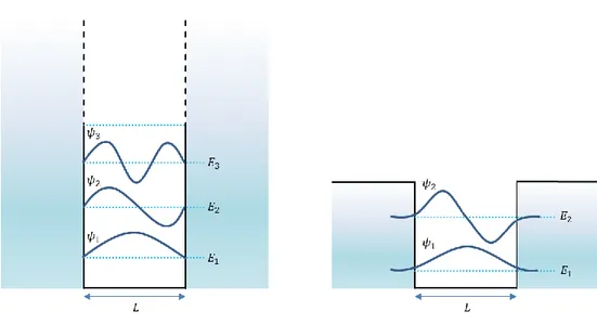
In this thesis, we showed device applications of semiconductor nanocrystals and, as we discussed, many novel properties of these nanocrystals originate from the quantum confinement. Here we start with an infinite square well problem, which is the most basic derivation of quantized energy levels. This is analogous to Fabry-Perot cavity for electromagnetic waves. Instead of a refractive index difference, there is a potential barrier. For an infinite square well having a well width 𝐿, discrete energy levels are characterized by an integer 𝑛 = 1, 2, 3, …
𝐸𝑛 =
𝑛2𝜋2ℏ2 2𝑚𝐿2
2.4 When we apply the infinite potential boundary conditions to the free electron, the wavefunction solutions become:
𝜓𝑛(𝑥) = √2 𝐿 sin ( 𝑛𝜋 𝐿 𝑥) 2.5 The first three energy levels and their corresponding wavefunction functions are illustrated in Figure 2.3 (left panel). Even the ground state has nonzero a energy and the wavefunctions are exactly zero at the potential barriers. An important result of the infinite well problem is the successful illustration of quantum confinement on the energy level separation: 𝐸𝑛 is inversely proportional to the square of the well width. Narrower
the well, higher the separation energies. This dependence is a direct consequence of quantum confinement. We observe this behavior with the size effect of nanocrystals:
smaller sizes of quantum dots (QDs) result in larger effective bandgaps, as we will discuss in the following sections.
Although, the infinite square well problem gives insight about the energy discretization, the infinite potential well is rather uncommon. Instead, a finite potential square well is more realistic and provides a good basic understanding on the core/shell heterostructures of nanocrystals. When coated over the core region, a higher bandgap shell creates a potential barrier for electrons and holes in the nanocrystal. The solution of the finite square well problem requires a slightly complicated approach and do not provide any significant understanding here. Instead, we will discuss the outputs of the solution. As shown in Figure 2.3 (right panel), wavefunctions inside the well have similar confined forms as the infinite well. However, above the potential barrier, electrons will be reflected and transmitted with corresponding probabilities, and they will be similar to free electrons. The states that reside within the energy of the well are the bound states and their energy levels change similar to the infinite well problem. Those outside the energy range of the well are the unbounded states.
There are two major observations for the finite well potential: there is always a bound state regardless of the potential depth and the particles always tunnel partially into the barrier. Indeed, the tunneling is another fascinating result of quantum formalism which classical physics cannot explain. Such tunneling of particles is an important concept to understand heterostructures of the semiconductor nanocrystals as well as various semiconductor devices.
Figure 2.3 Illustration of infinite (left) and finite (right) square potential well problems for a particle with mass.
2.3 Density of States for Electrons and Holes
Absorption and emission processes in quantum emitters can be explained by using Fermi’s golden rule. Quantum mechanical absorption rate for each allowed transition between discrete states is given by:
𝑊𝑖→𝑗 = 2𝜋 ℏ |⟨𝑖|𝐻 ′|𝑗⟩|2𝛿(𝐸 𝑗− 𝐸𝑖− ℏ𝜔) 2.6 For continuum of states observed in semiconductors, Fermi’s golden rule becomes
𝑊𝑖→𝑗 =
2𝜋 ℏ |⟨𝑖|𝐻
′|𝑗⟩|2𝑔(ℏ𝜔)
where 𝑔(ℏ𝜔) is the density of available states. [15] The unitless term |⟨𝑖|𝐻′|𝑗⟩|2 is called
the oscillator strength related to the strength of the corresponding oscillation among all allowed oscillations in the system. 𝐻′ is the interaction Hamiltonian between the states 𝑖
and 𝑗. Using Fermi’s golden rule for the upward transition (absorption process) and the downward transition (emission process), as a directly measurable quantity, we can calculate absorption coefficient (which is given per length) denoted as 𝛼 for direct bandgap semiconductors. The difference between the upward and downward transitions per unit number of incident photons gives the net absorption [16]
𝛼(ℏ𝜔) = ℏ𝑒 2 2𝑚0𝑐𝜖0 1 𝑛𝑟 𝐸𝑝 ℏ𝜔𝑔𝑗(ℏ𝜔)[1 − (𝑓𝑒+ 𝑓ℎ)] 2.8 where 𝑛𝑟 is the refractive index, 𝐸𝑝 is a material parameter that comes from k•p theory,
and 𝑔𝑗(ℏ𝜔) is the joint density of states of electron and hole. 𝑓𝑒 and 𝑓ℎ are Fermi
distributions of electrons and holes at the corresponding energy level and temperature defined as 𝑓𝑒(𝐸, 𝑇) = (1 + 𝑒 𝐸−𝜇 𝑘𝐵𝑇) −1 , 𝑓ℎ(𝐸, 𝑇) = 1 − (1 + 𝑒 𝐸−𝜇 𝑘𝐵𝑇) −1 2.9 As stated, the absorption and emission processes of a semiconductor are directly related with the electronic band structure. Changing the carrier concentrations, hence the Fermi levels, can also modify the material properties significantly. It is possible to adjust the carrier concentration by changing the temperature and or by applying external electric
field, which in turn change the chemical potential 𝜇. Under intense electrical or optical pumping, Equations 2.9 change significantly and 1 − (𝑓𝑒+ 𝑓ℎ) term becomes negative
in Equation 2.8, meaning that there is a net optical gain induced in the semiconductor instead of optical absorption. This relation is useful to understand the basic conditions to achieve optical gain in semiconductors.
Using this absorption coefficient and Einstein coefficients, the spontaneous emission rate per unit volume can be found as
𝑟𝑠𝑝𝑜𝑛𝑡(ℏ𝜔) =
8𝜋𝑛𝑟2
ℏ3𝑐2[ℏ𝜔]2𝑓𝑒𝑓ℎ𝛼(ℏ𝜔)
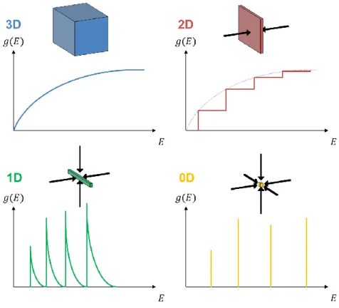
2.10 In both the absorption and emission processes, the density of states has critical importance and strongly depends on the dimensionality of quantum confinement. To understand optical properties of highly confined nanocrystals in different shapes, we need to understand the density states behavior of carriers.
The solution for the density of states requires to work in the reciprocal space under the infinite crystal approximation. Three-dimensional reciprocal space wavevector components for lattice constants 𝑎, 𝑏 and 𝑐 are
𝑘𝑥 = 𝜋 𝑎, 𝑘𝑦 = 𝜋 𝑏, 𝑘𝑧 = 𝜋 𝑐 2.11 In the reciprocal space, the density of states 𝑔(𝑘) is defined as 𝑔(𝑘) = 𝑑𝑛/𝑑𝑘. In three-dimensions, 𝑛 is the number of states per real unit cell volume defined (𝑉 = 𝑎𝑏𝑐) as
𝑁 = 2Ω 8𝑘𝑥𝑘𝑦𝑘𝑧 = 𝑉𝑘 3 3𝜋2 , 𝑛 = 𝑁 𝑉 = 𝑘3 3𝜋2 2.12 where Ω is the octant of the reciprocal space
Ω =4𝜋 3 𝑘
3
2.13 and since the total number of states are fixed, 𝑔(𝐸)𝑑𝐸 = 𝑔(𝑘)𝑑𝑘. Using the wavenumber and energy relation for a particle, we have
𝑘 =√2𝑚𝐸 ℏ , 𝑑𝑘 𝑑𝐸= 1 ℏ√ 𝑚 2𝐸 2.14 and the resulting three-dimensional density of states 𝑔3𝐷 is calculated as
𝑔3𝐷(𝑘) = 𝑘2 𝜋2, 𝒈𝟑𝑫(𝑬) = √2𝑚3(𝐸 − 𝐸𝑔) 𝜋2ℏ3 2.15 In bulk form, semiconductors have 1/2 power dependence on the energy as sketched in Figure 2.4.
The two-dimensional density of states is the case under strong quantum confinement in one dimension. We have a real space unit cell area (𝐴), the quadrant of reciprocal space for calculations and the number of states per unit cell area as follows
𝐴 = 𝑎𝑏, Ω = 𝜋𝑘2, 𝑁 = 2Ω 4𝑘𝑥𝑘𝑦 =𝐴𝑘 2 2𝜋 , 𝑛 = 𝑁 𝐴 = 𝑘2 2𝜋 2.16 The resulting two-dimensional density of states 𝑔2𝐷(ℏ𝜔) is give by
𝑔2𝐷(𝑘) = 𝑘 𝜋, 𝒈𝟐𝑫(𝑬) = 𝑚 𝜋ℏ2 2.17 which is energy independent. Under quantum confinement, each state energy will have abrupt jumps creating a series of step functions as shown in Figure 2.4.
Under the two-dimensional confinement, the one-dimensional density of states can be calculated using unit cell length 𝑙 and half of the reciprocal space
𝑙 = 𝑎, Ω = 𝑘, 𝑁 = 2Ω 2𝑘𝑥 =𝑙𝑘 𝜋 , 𝑛 = 𝑁 𝑙 = 𝑘 𝜋 2.18 The one-dimensional density of states is then
𝑔1𝐷(𝑘) = 1 𝜋, 𝒈𝟏𝑫(𝑬) = 1 𝜋ℏ√ 𝑚 2(𝐸 − 𝐸𝑔) 2.19 Equation 2.19 shows the inverse square root energy dependence within and, like 𝑔2𝐷(ℏ𝜔), here the quantum confinement creates discrete energy states within this
the zero-dimensional QDs, 𝑔0𝐷, consists of delta functions at the corresponding
quantized energies as shown in Figure 2.4.
Figure 2.4 Different dimensionalities and their corresponding density of states illustrated from bulk to 0D.
In Figure 2.5, Fermi distributions at the absolute zero and elevated temperatures are illustrated. Since the net absorption coefficient 𝛼 is a product of (1 − 𝑓𝑒− 𝑓ℎ) and 𝑔𝑗,
the change in the number of states with temperature is also shown here. 𝑁(𝐸) with respect to 𝐸 for 𝑇2> 0 K case is quite similar to the absorption tail of semiconductors.
Figure 2.5 The product of Fermi distribution and the density of states determines the absorption profile. The product of (1 − 𝑓(𝐸)) and the three-dimensional density of states (𝑔3𝐷(𝐸)) at 𝑇2> 0 K successfully illustrates a typical absorption tail of a semiconductor.
2.4 Colloidal Semiconductor Nanocrystals
Semiconductor nanocrystals can be obtained using different methods. Before colloidal synthesis of QDs, QDs were obtained in molten glass and their optical properties were correctly attributed to the quantum confinement effects. [17] the first systematic studies have been performed on these quantum confined nanocrystals, however, this method had inherently limited control over the shape, material composition and uniformity of the structures. These initial studies paved the way for semiconductor nanocrystal research and showed promising properties of nanocrystals including strong absorption [18], tunable PL emission even from indirect bandgap materials [19], and strong optical gain performance [20], which attracted attention of researchers and engineers. After the first colloidal synthesis of semiconductor nanocrystals, [1] tremendous research efforts have been made, which allowed for different sizes, various shapes and alloyed compositions of semiconductor nanocrystals. After 30 years of research, the commercialization of
colloidal QDs has created a promising market especially as primary color convertors in electronic displays. [7]–[9] The capability of size and shape control of nanocrystals through solution-processed synthesis methods make advanced heterostructures possible. Zero-dimensional atom-like QDs [1], one-dimensional quantum rods (nanorods) [21], [22]and two-dimensional quantum wells (nanoplatelets) [23]together provide us with an exciting toolbox for nanocrystal research.
In Figure 2.6, the effect of quantum confinement on semiconductor energy band diagram is shown. Unlike a continuous energy band diagram presented in Figure 2.2, the discretization of energy levels allows only certain transitions and due to the sharp curves of conduction and valence bands around the bandgap, the number of possible transitions is limited. This limited number of states require interaction of electrons and holes through the higher energy states, hence effectively leading to an increase in the energy bandgap.
Figure 2.6 Effect of quantum confinement on bulk semiconductor energy band diagram given in Figure 2.2. Quantization restricts only certain k values on the band diagram.
𝐸 𝑘 Conduction Band Valence Bands Heavy-hole Light-hole Split-off 𝐸𝑔
The sizes of nanocrystals is in the order of exciton Bohr radius. Since an exciton is a quasi-particle consisting an electron and a hole, it resembles a hydrogen atom. [24] the 1s orbital energy of hydrogen and its orbital radius (Bohr radius) can be calculated for an exciton in bulk semiconductor as
𝐸𝑒𝑥= 1 4𝜋𝜖0 𝜇𝑒4 2𝜖2ℏ2 2.20 𝑎𝐵∗ = 4𝜋𝜖0 𝜖ℏ2 𝜇𝑒2. 2.21 In Equations 2.20 and 2.21, 𝜖 is the dielectric constant of the semiconductor medium and 𝜇 is the reduced effective mass of the electron-hole pair. Under the one-dimensional confinement, 𝐸𝑒𝑥 and 𝑎𝐵∗ take their two-dimensional form related to their
three-dimensional values as [25]
𝐸𝑒𝑥,2𝐷= 4𝐸𝑒𝑥,3𝐷, 𝑎𝐵,2𝐷∗ =
𝑎𝐵,3𝐷∗
2
2.22 Four-fold increase in the exciton binding energy is a strong modification for two-dimensional systems and allows to observe strong excitonic features in the absorption spectrum even at room temperature. Generally low exciton binding energies of semiconductors are below 𝑘𝐵𝑇 value at room temperature (~26 meV) and cannot be
observed in the absorption spectrum. In Chapter 5, colloidal quantum wells will be introduced and their quasi-two-dimensional nature dictates an exciton binding energy
between 𝐸𝑒𝑥,2𝐷 and 𝐸𝑒𝑥,3𝐷. Heavy-hole, light-hole and split-off excitonic features are
clearly visible in their absorption spectra.
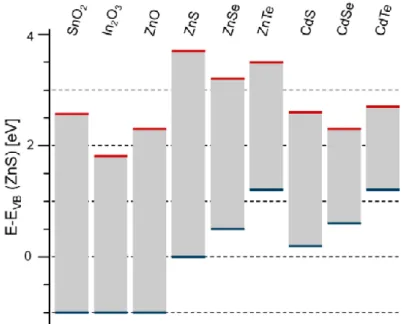
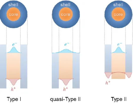
In addition to the size tuning to control the electronic band structure of nanocrystals, heterostructures can add another degree of freedom for the-so-called bandgap engineering. In Figure 2.7, bandgaps and relative positions of the band offsets are shown for commonly used semiconductor compounds. Effective positioning of different materials allows for designing nanocrystals with high stability [3]–[5], enhanced optical gain performance [26], extremely Stokes-shifted emission and increased charge separation [2], [6]. Different combinations of heterojunctions are illustrated in Figure 2.8. According to the barrier height, the localization of electrons and holes varies. Like core-only nanocrystals, the localization of electron and hole in the same core region is referred to as Type I structure. The opposite is also possible when the localization of both carriers occurs in the shell region, which is known as the inverse Type I. When carriers are separated in different regions of the nanocrystal, e.g., electrons in the core and holes in the shell or vice versa, the structure exhibits Type II band alignment. If the barrier is shallow for one carrier allowing to delocalize through the entire structure and the other carrier is strongly localized in one region, the structure is called as quasi-Type II structure. This control over the distributions of the carriers changes the overlap between them and directly effects the oscillator strength. For example, while the oscillator strength is quite strong in Type I structures, this tight confinement in the same region increases the nonradiative Auger recombination losses, creating a killer effect for the optical gain performance. Type II and quasi-Type II band alignments offer a remedy for Auger recombination at a cost of considerably reduced oscillator strength and broadened PL emission. In Figure 2.9, various different types of CdSe quantum well
colloids are shown under ambient and UV illumination exemplifying the possible engineering of the absorption and emission properties of these nanocrystals.
Figure 2.7 Bandgaps and relative band alignments of commonly used semiconductors for colloidal nanocrystals. After [27] © IOP Publishing. Reproduced with permission. All rights reserved.
Figure 2.8 Illustration of different types of the band alignments and their corresponding electron and hole wavefunction across the heterostructures of each nanocrystal.
Figure 2.9 Various 4 ML Type I and Type II CQWs under ambient lighting (top) and UV illumination (bottom) showing bright colors all across the visible spectrum from green to red (Demir Group).
2.5 Plasmonics: Colorful Metals of Nanoworld
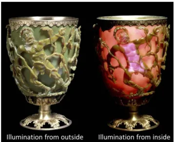
Semiconductor nanocrystals show novel physical properties at the nanoscale thanks to the quantum confinement. In metals, electrons are nearly free and does not experience periodic potential of ordered atoms as electrons do in semiconductors. Yet, physical properties of metals significantly change at the nanometer scale as well. One of the first observations was the color change in the beaten metallic leaves of gold and silver by Michael Faraday in 1857. [1] This effect was due to the collective oscillations of nearly-free electrons inside the tens of nanometers thick metallic films. Like a plasma, electrons are free to move in a collective oscillation at a frequency called plasma frequency in bulk form. Hence the name plasmon is coined for the quanta of collective electron oscillation in an electron-rich material and plasmonics has become one of the very active fields of nanoscience research. [28] One of the first applications of plasmonic interactions goes back to the 4th century AD. Lycurgus Cup is one of well-known ancient artifacts in
plasmonics community, for it can change its color depending on the illumination location. As shown in Figure 2.10, when illuminated from the inside, the cup is red and its color changes to green when illuminated from outside. This is the result of absorption and scattering behavior of the metallic nanoparticles embedded in the glass. Such metallic nanoparticle-incorporated glasses are still being used for stained glass manufacturing but this time we know its underlying physics.
Figure 2.10 The first known example of a plasmonic application: Lycurgus Cup. Dichroic behavior of the glass is originated from the incorporated metallic nanoparticles. © Trustees of the British Museum [29].
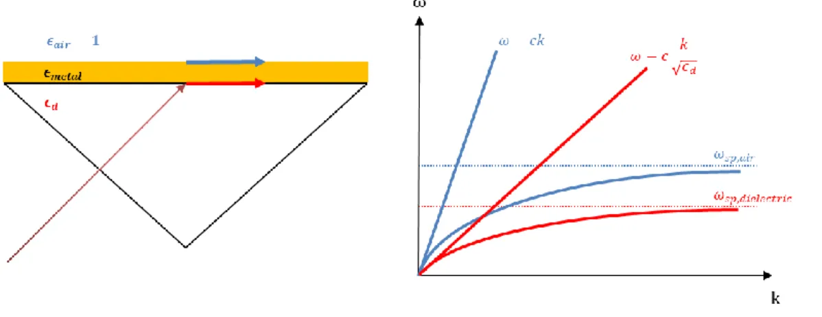
Bulk volume plasma frequency (𝜔𝑝) of electrons in a metallic structure depends on
the number of electrons per unit volume (𝑛) and the effective mass of electron in the material (𝑚𝑒𝑓𝑓):
𝜔𝑝2=
𝑛𝑒2 𝜖0𝑚𝑒𝑓𝑓
2.23 Equation 2.23 gives the resulting frequency of the nearly free electron oscillations under the restoring force created from the electric field of electron motion in Drude model. The solution to this restoring force problem comes from a simple harmonic oscillator and it is purely classical. Even though the plasmonic effects can be observed at the nanometric scale, the plasmonic response of metals can be predicted by classical mechanics with high precision. Quantum mechanics is only involved in the density of electrons and