.лій:і!іС*гіУсі/й^0 о і У г 2£ í é s ’'P.P''í / /** т<і i¡¿ -W W * J 'J J I Iw ^ '■^· *i «Ir {· Г-Л* 'Я*»Ѵ. .-^'T ** J V Ί ’■?
m
PARTIA!, FTLFIJuLMËMT ’.Г;■*, VT - ~ . > i/ -··; г ,· · «,*. ^ ·AUGa,_:,As/GaAs GRADED INDEX SEPARATE
CONFINEMENT HETEROSTRUCTURE SINGLE
QUANTUM WELL LASERS
A THESIS
SUBMITTED TO THE DEPARTMENT OF PHYSICS AND THE INSTITUTE OF ENGINEERING AND SCIENCE
OF BILKENT UNIVERSITY
IN PARTIAL FULFILLMENT OF THE REQUIREMENTS FOR THE DEGREE OF
MASTER OF SCIENCE
By
Miimtaz Koray Bozkurt
February 1994
(9 9 ί|
I certify that I have read this thesis and th at in my opinion it is fully adequate, in scope and in quality, as a thesis for the degree of Master of Science.
Prof. Atilla Aydınlı (Supervisor)
I certify th at I have read this thesis and th at in my opinion it is fully adequate, in scope and in quality, as a thesis for the degree of Master of Science.
/
c
Prof. Atilla Erjelebi
I certify that I have read this thesis and th at in my opinion it is fully adequate, in scope and in quality, as a thesis for the degree of Master of Science.
Assoc.Prof. Recai Ellialtioglu
Approved for the Institute of Engineering and Science:
Prof. Mehmet Bara^
A b stract
AU G ai-.A s/G aA s GRADED INDEX
SEPARATE CONFINEMENT HETEROSTRUCTURE
SINGLE QUANTUM WELL LASERS
Mümtaz Koray Bozkurt
M. S. in Physics
Supervisor: Prof. Atilla Aydınlı
February 1994
"Stimulated emission of photons could be produced in semiconductors by recombination of carriers injected across a p-n junction
This idea was first suggested by Basov et al} in 1961. Soon afterwards diode lasers were first demonstrated at cryogenic temperatures in pulsed operation in 1962 by separate groups in US.^"® Until the first use of heterostructures in diode la s e rs ^ in 1969, advances in the diode laser area were not as good as was expected. New era of the diode Icisers begin with use of the heterostructures in laser diode technology which allowed them to run at room temperatures in continuous wave operations. Also, introduction of MBE and LPE techniques in crystal growth area supplied the forecoming materials and enabled growing of nanocrystal layers for semiconductor laser diode applications. Reaching to reliable, compact and an efficient components for applications is the major factor which forces the laser diode designs to maturity.
In this work, ridge type Single Quantum Well Graded Index Separately Confined Heterostructure lгıser diodes which were made by reactive ion etching in CCI2F2 and lift-off of low temperature PECVD SİO2, is taken from its crystal growth aspects through design and fabrication steps to its characterization.
K eyw ords : Laser diode, single quantum well, graded-index. Gallium Arsenide, plasma enhanced chemical vapor deposition (PECVD).
ö z e t
A l,G aı-,A s/G aA s DEĞİŞKEN KIRILMA İNDİSLİ
AYRIK HARİSLİ HETEROYAPI
TEK KUVANTUM KUYULU LAZERLER
Mümtaz Koray Bozkurt
Fizik Yüksek Lisans
Tez Yöneticisi: Prof. Atilla Aydınlı
Şubat 1994
“Yarıiletkenlerde uyarıirruş foton yayımı yük taşıyıcılarının p-n eklemi üzerinden basılması ile elde edilebilir.”
Bu fikir ilk defa Basov ve arkadaşları’ tarafından 1961 de önerilmiştir. Kısa bir sûre sonra düşük sıcaklıklarda darbeli olarak çalışan ilk lazer diyotlar A.B.D. de farklı birkaç grup^“® tarafından gerçekleştirilmiştir. Heteroyapıların 1969 da ilk defa liizer diyot yapımında kullanılmasına kadar®^ bu alandaki gelişmeler beklendiği ölçüde olmamıştır. Lcizer diyot teknolojisinde heteroyapıların kullanımı ile birlikte oda sıcaklığında sürekli çalışabilen lazerlerin elde edilmesi bu teknolojide yeni bir dönem açmıştır. M BE ve LPE tekniklerinin kristal büyütme alanına girmesi, yarıiletken lazer diyot uygulamaları için nanokristal tabakaların büyütülmesine olanak sağlamıştır. Uygulamalar için güvenilir, küçük ve verimli elemanların elde edilmesi lazer diyot tasarım teknolojisini olgunluğa sevk eden faktörlerdir.
Bu çalışmada, CCI2F2 ile reaktif iyon aşındırma ve alçak sıcakhklarda plazma ile hızlandırılmış kimyîisal fazdan büyütülen SİO2 in kaldırılması ile elde edilen sırt şerit tipi tek kuvantum kuyulu değişken kırılma indisli ve ayrık hapisli heteroyapı lazer diyotlarm, tasarımı, üretimi ve karakterizasyonu aşamaları gerçekleştirilmiştir.
A n a h ta r K elim eler : Lazer diyot, tekli kuvantum kuyu, degi§ken ktnima indisi. Galyum Arsenit, plazma ile hızlandırılmış kimyasal fazdan depolama.
A cknow ledgem ent
My sincere thanks are due to my parents for their understanding, moral support, and especially for their patience.
I would like to express my gratitude to my supervisor Prof. Atilla Aydmb for his constant guidance and encouragement throughout this work. I would like to thank to Assoc. Prof. Recai Ellialtioglu for his help. I appreciate the support provided by A.F. Ioffe Physico-Technical Institute and the members of the Optics Laboratory. I wish to express my special thanks to senior research scientist Feodor N. Timofeev.
I would like to thank to my colleague A. Kamuran Tûrkoğlu for his collaboration. Many thanks to process engineer Murat Güre and to our laboratory technician Güngör Sincer for their help in this work.
This project was performed under the auspices of Ministry of Defense, Undersecretariat for Defense Industries, Grant No: SSM-90-033.50.
C ontents
A bstract O zet 11 Acknowledgem ent 111• ·· C ontents IV List of Figures v il1 History and Evolution of Laser D iodes 1
2 Heterojunotions and Quantum Well Lasers 6
2.1 Heterostructures ... 6
2.2 Quantum Well S tr u c tu r e s ... 9
2.3 Separate C o n fin em en t... 15
3 Process 17 3.1 Laser Diode S tr u c tu r e ... 17
3.2 Cleaning and Wafer preparation... 18
3.3 Photolithography... 20
3.3.1 Photoresists... 22
3.3.2 P rin tin g ... 22
3.3.3 E xperim ental... 23
3.3.4 Process n o t e s ... 27
3.4 Reactive Ion Etching ( R I E ) ... 28
3.5 Anodic O xidation... 36
3.5.1 Process n o t e s ... 37
3.6 PECVD and Lift off of Si0 2 ... 39
3.7 M etalization... 48
3.7.1 T hinning... 49
3.7.2 A n n e a lin g ... 51
4 Characterization 53 4.1 Laser diode p aram eters... 53
4.2 I-V Characterization and Series resistance R , ... 54
4.3 Emission spectra of the G R IN S C H ... 56
4.3.1 Optical resonant cavity and its m odes... 56
4.3.2 Effect of operating temperature on the emission wavelength 58 4.4 I-P Characterization ... ... 59
4.4.1 Threshold C u r r e n t ... 60
4.4.2 Differential quantum efficiency i/d ... 65
4.5 Spontaneous Emission and L a s i n g ... 68
4.6 Far Field P a t t e r n ... 72
4.7 Near Field P a t t e r n ... 75
5 D iscussion and Conclusions 78
List o f F igures
1.1 Laser with a Fabry Perot resonator... 1 1.2 Broad-contact semiconductor l<iser mounted on heat sink, with
lead wire... 2 2.1 (a) The band diagram of two different disconnected semiconduc
tors 1 and 2, with energies shown relative to the vacuum. The line up of band structures of lattice-matched semiconductors 1 and 2 forming a heterojunction. It is assumed th at materials are undoped and that the effect of charge transfer at the interface is negligibly small... 7 2.2 Infinitely deep quantum-well energy levels and wave functions. . . 11 2.3 First two bound energy levels and wave functions in a finite
quantum w e l l ... 12 2.4 Graphical solution of the energy levels for a finite well Solutions
are the intersections of the straight line with slope k~^ with curves y = cos{kL/2) (with tan(A:L/2) > 0 ; ---; even wavefunctions) or y = sin{kL/2) (with ta,n(kL/2) < 0 ; --- ; odd wavefunctions. 13 2.5 1-e to Ihh Transition energy vs. Quantum well w i d t h ... 14 2.6 1-e to llh Transition energy vs. Quantum well w i d t h ... 15 2.7 Confined energy levels for a 39
A
thick quantum well... 16 3.1 Layers and basic energy band diagram of SQW-GRINSCH . . . . 18 3.2 SEM micrograph of S Q W -G R IN S C H ... 19 3.3 (100) oriented GaAs wafer illustrating cleavage planes andanisotropic as evidenced by a raised mesa and etched slots . . . . 20
3.4 Schematic of refractive optics reduction projection printer... 21
3.5 Positive and Negative Photoresist behavior after the develop . . . 22
3.6 Mercury lamp output for resist exposure... 23
3.7 Basic schematic of MJB-3 UV-300 Mask A l i g n e r ... 24
3.8 Basic schematic of R I E ... 28
3.9 Isotropic(left) and anisotropic e tch in g (rig h t)... 30
3.10 A parallel-plate ” Reinberg” style reactor with radial gas flow. . . 31
3.11 Dependence of on RF power (RIE) for O2 and CCljFj; P= 0.8 P a ... 32
3.12 Profiles of the 5/xm and I2fim stripes: (a) Before etching (b) After first etching step... 34
3.13 Etching profiles of the 5/im and 12/xm stripes after second etching step... 35
3.14 Anodic oxidation setup... 37
3.15 Oxide etching characteristic of H C L ... 38
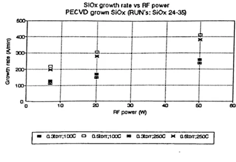
3.16 Parallel plate /ip-Dp80 plasma reactor in PECVD configuration . 40 3.17 SiOi Films on Si p-type (100). D ata in parenthesis indicate the thickness
of
the film inA
... 423.18 IR absorption spectra for thermally grown films at 1 atm of dry oxygen a t temperatures of 700, 800 and 1000“C. 0 atom motion for rocking, bending and stretching vibrations are also indicated . 43 3.19 SiO*-24 absorption spectra ... 44
3.20 RF power (W) vs. Growth Rate
(A/min)
... 473.21 Thinning characteristic of GaAs wafers in Ammonia sol.+ H2O2 (1:10) ... 50
4.1 I-V Characteristic of the GRINSCH Laser Diode ... 55
4.2 Lasing emission spectra of the GRINSCH laser d i o d e ... 57
4.3 Dependence of the band-gap energy of GaAs on temperature. . . 58
4.4 I-P Measurement setup ... 59
4.5 I-P charticteristic of GRINSCH ... 60
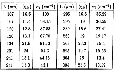
4.6 Jtfc vs. L (a) For 5pm stripe width (b) For 12pm stripe width . . 62
4.7 Ijfc vs. L (a) For 5μη\ stripe width (b) For 12/im stripe width . . . 63 4.8 Schematic of the waveguide and reference coordinates... 64 4.9 1/Differential Quantum Efficiency Ι/η ο vs. cavity length L, (a)
For 5/im stripe width (b) For 12μτη stripe width... 66 4.10 Spontaneous emission spectra at different cavity lengths. Peak
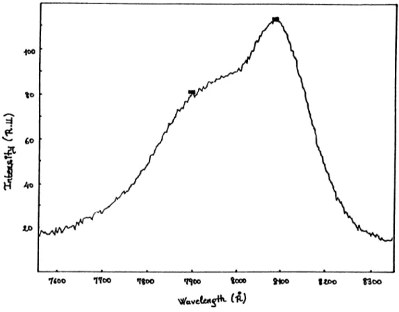
positions of the spectra are shown by rectangles... 68 4.11 Spontaneous emission spectra at 804/im cavity length is showing
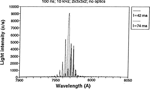
two transitions between the edges of the le -llh subbands and Ιο ί hh subbands... 69 4.12 Lasing emission spectra of GRINSCH at two different current values. 70 4.13 Alignment setup for far field measurement ... 73 4.14 Lateral Far Field patterns for GRINSCH laser diodes. (a)
L=563/xm w=5/xm (b) L=429/xm w=12/im... 74 4.15 Transverse Far Field pattern for δβΖμτη long 5μτη stripe width
laser diode... 75 4.16 Near field measurement s e t u p ... 76 4.17 Near Field pattern of the GRINSCH Iciser diode, L=563/im w=5^m 77
C hapter 1
H istory and Evolution of Laser
D iod es
The basic structure of a laser consists of an amplifying medium with inverted population between two mirrors Ml and M2 (figure 1.1). The two mirrors constitute a Fabry Perot resonator which confines light at a resonant frequency. Beside Bragg reflectors, diffraction gratings and plane mirrors can also be used internally and externally in such a configuration.
In normal state of the medium there are more electrons in the lower level than in the upper one and stimulated emission and absorption occur simultaneously. If medium is excited by an appropriate method so that upper level contains more
< - --- L --- --- >
/
Medium with inverted population
Laser output
Chapter 1. History and Evolution o f Laser Diodes
F ig u re 1.2: Broad-contact semiconductor laser mounted on heat sink, with lead wire.
electrons than the lower one (population inversion) light incident on the medium will be·" amplified by stimulated emission. Population inversion is obtained in semiconductor injection lasers easily by injecting current through the contacts.
First injection lasers were made from rectangular shaped GaAs p-n junctions diffused in planar form. Output connections were taken from the top and metal base where the chip was set (figure 1.2). When current is injected into such a structure, like in normal p-n diode, minority carriers (electrons) come to the junction where thickness is on the order of the diffusion length of the electrons, and they recombine with the majority carriers (holes) and light is emitted. Stimulated emission starts in the junction area when the current density reaches to a sufficient level (threshold level).
Because of the index of refraction difference between the GaAs and air at the cleaved facets (cleaved mirror faces) light is confined inside the medium selecting its Fabry Perot resonance frequency. High rate of stimulated emission in semiconductors allows us to choose the length of Fabry Perot as small as a few hundred microns. Todays semiconductor lasers are based on the same p-n
Chapter 1. History and Evolution o f Laser Diodes
junction principle and they are represented by the diode symbol.
In such structures threshold current densities lie in the range of 35-100 kA/cm^. This high current originates from the high density of states in valence and conduction bands in the bulk material. However light is by no means confined to the area of inversion. Also one can not define an exact region of inversion for the carriers.
Putting additional layers of higher bandgap materials to each side of GaAs p-n junction was proposed by Kroemer® and Alferov and Kazarinov.*® Such a design provided the confinement of injected carriers to the active region (p-n junction area) and substantially increased the confinement of light to the same region. Injected carriers are kept in the active region by the difference of bandgap energies while inverse relationship between bandgap energy and refractive index gives us the definition of a waveguide for generated light. MBE and LPE crystal growth techniques enabled the growth of higher bandgap ternary elements to be used in laser diodes. Confinement of carriers and the light substantially increased the rate of inversion resulting in a decrease of threshold currents. If higher bandgap material is grown to one side of the active region this design is called single heterostructure, suitable for high power outputs. If the higher bandgap material is grown to either sides of active region it is called double heterostructure, which is suitable for low threshold currents and continuous wave operations.
One of the important things in semiconductor laser diodes is to limit the spread of injected carriers and lasing emission in the plane parallel to the junction. This is achieved by confining the carriers to narrow stripes (from few microns to few tens of microns) aligned along the axis of the laser. To stop carriers outside the stripe areas, different insulating techniques can be used. One such a configuration is called stripe geometry lasers. Dielectric deposition is one of the famous ways to achieve this geometry. In buried type structures proton bombardment can also be used as a process step.
Most of the III-V semiconductors has the inverse relation between refractive index and their bandgaps. Using this fact, contemporary technology offers real confinement of light into active region. By changing the atomic composition of
Chapter 1. History and Evolution o f Laser Diodes
materials in MBE, energy gaps and refractive indices can be adjusted. If one puts multilayers of such materials step by step to each side of active region, refractive index of the confining layers can be adjusted in the desired shape to form the waveguide. This technique is called index-grading.
With the advent of novel crystal growth techniques such as Molecular Beam Epitaxy (MBE), Metalorganic Chemical Vapor Deposition (MOCVD) and alike, active region thicknesses went down to quantum sizes and new type of semiconductor laser diodes, QW lasers, are fabricated by this means.
These lasers show a number of interesting properties th at distinguish them from other types of junction lasers. Their most important characteristics include the following features; low density of the threshold current Tsang** 1981, Fujji et alP 1984, the small variation of the threshold current with tem perature Chin et alP 1979, Hess et a lP 1980, Arakawa and Sakaki **1982, possibility of tuning the emitted wavelength over a wide range, extending up to 100 nm, by varying the driving current, good dynamic charax:teristics, Arakawa et a lP 1984, Arakawa and Yariv.*'^
In the initial stage of the QW laser studies Liquid Phase Epitaxy (LPE) wais used in layer growths. Good quality single QW lasers were fabricated by Rezek et a lP by using LPE in 1977. Historically, the first QW lasers of really satisfactory performance have been fabricated by the MOCVD technique by Dupuis and Dapkus*® and Dupuis et a l.P Kazarinov and Tsarenkov^* (1976) show theoretically th at using index grading technique in the confining layers lowers the threshold currents of the conventional separate confinement structures.
In 1981 Tsang** used MBE growth technique in fabrication of multilayer GaAs/Ali:Gai_xAs lasers with threshold current densities of the order of 800 A/cm^, which are comparable with the values obtained in the conventional Double Heterostructure Lasers containing Alj;Gai_a,As confining layers with a similar A1 content. Gain guided stripe-geometry quantum well lasers operating in continuous wave mode a t room temperature with 30 mA threshold current were demonstrated by Tsang.**
Chapter 1. History and Evolution o f Laser Diodes
special design, in which the conhning layers of varying composition enhance the efficiency of the carrier capture by the active region. In this study threshold current densities below 300 A/cm* W eis achieved.
In parallel with these studies a model on threshold current in QW lasers was proposed by Dutta^^ (1982) and an accurate model for the gain in QW structure was shown by Asada et cd?* (1985). The effect of gain saturation at high injection currents by Arakawa and Yariv^® (1986) and the relation between the threshold current and width of the active region layer by Hersee et al?^ (1984) have been confirmed. Single quantum well broad contact GRINSCH lasers with 380-1125 pm cavity length, made by MBE have been reported by Tsang^^ to show threshold current densities ranging from 250 A/cm^ to 160 A/cm^ with external incremental quantum efficiencies from 32 to 40 % (one mirror efficiency). Stripe contact GRINSCH lasers of 5 /im stripe width and 380 pm cavity length giving 10 mW per mirror in cw operation have also been demonstrated by Tsang and Hartman^^ (1983). In buried type GRINSCH lasers 2.5 mA threshold current has been reported by Tsang,*^ and Derry et a/.^(1987) have been fabricated lasers with submiliampere threshold currents. Sheally** demonstrated superlattice GRINSCH lasers operating in the range of 700 to 845 nm with high efficiency 40 % (one mirror)(1988). AlxCai-^As/GaAs single QW ridge type GRINSCH lasers with power outputs of 425 mW (one mirror) at 856 nm were fabricated, and 428 nm frequency-doubled output of 41 mW was demonstrated by Jaeckel et al.?^
C hapter 2
H etero ju n ctio n s and Q uantum
W ell Lasers
2.1
Heterostructures
In semiconductor literature, when two different semi-infinite semiconductor crystals are joined together, the interface is called heterojunction and the resultant structure is the heterostructure. Crystal structure and the crystal potential doesn’t change in bulk areas and abrupt change is seen only at the heterojunction. This is an assumption for the cases in which lattice constants of the materials differ very little for similar materials. By this assumption lattice constant can be taken as a parameter for semiconductors forming heterostructures. Fortunately most of the important semiconductors have zinc- blende and diamond symmetry and are therefore quite compatible provided the lattice constants are similar.
Relative positions of constituent band structures of the heterojunction system provides the band offsets (potential step at the interface figure 2.1). Since mean electron charge density must be the same for both sides of the interface, Fermi energy which depends on it lies in the middle of the gap. Small differences in electron density due to different lattice constants are removed by charge transfer across the interface.
Chapter 2. Heterojunctions and Quantum Well Lasers % ■"gi Wi -Ef -///// (a) Wz iZ Z / / / / / / / / / ^92 //////// \//////// -Epf--- Ef^ -177777777 77777777 ] AEy (b )
F ig u re 2.1: (a) The band diagram of two different disconnected semiconductors 1 and 2, with energies shown relative to the vacuum. The line-up of band structures of lattice-matched semiconductors 1 and 2 forming a heteroj unction. It is assumed that materials are undoped and that the effect of charge transfer at the interface is negligibly small.
To get valence band-offset AE„,
A F „ = { E g X — E g 2 ) l 2
If we attem pt to use this model and above expression directly for conduction band-offset it fails since conduction band has several minima and in some cases indirect gaps being smaller than direct ones. Once we obtain the valence band offset AE„ conduction band offset AEc is,
AFc = \Egx - Eg2\ - IAE„|
Eji and Ej2 are now the experimental values of the fundamental gaps of the two bulk constituents. If both constituents are direct gap materials, above expression is enough to find AEc, subtraction of the energies of the conduction minima th at are alike. In our consideration electron passes at the interface from r to r or X to X valleys even though in some cases X lies below F.
For electrons F to X valley transfer cannot be used at the interface since abrupt change of electron momentum must take place.“ Probability of a P electron approaching the interface and seeing the X valley is very small. In this way, electron interau:tion at the interface can be modeled as a reflection from a step-like barrier. By using empirical bulk material energy gap values and lattice constants,“ band offsets for any pair of heterostructures which have small lattice mismatches can be found. Some of the experimental constants for GaAs and AlxGai_iAs are given in the table below.
Chapter 2. Heterojunctions and Quantum Well Lasers 8
GaAs AlxGai_j;As
Lattice constant a(A) 5.6533 5.6533 + 0.007&T Bandgap Energy (eV)
r valley minima
1.424 1.424 -f- 1.247a: from a:=0 to a:=0.45 1.900 + 0.125x -1- 0.143x2 from x = l to x=0.45
Static dielectric constant e. 13.18 13.18-3.12x
High Frequency dielectric constant 10.89 10.89 - 2.73x LO phonon energy (meV) 36.25 36.25 - 6.55x -1- 1.79x2
GaAs type 44.63 -I- 8.78x - 3.32x2 AlAs type
Chapter 2. Heterojunctions and Quantum Well Lasers
2.2
Quantum Well Structures
As we mentioned in evolution of the laser diodes, if we grow a very thin layer of material A (such as GaAs) between two thick higher bandgap material B (such as AliGai_*As) these three layers form a double heterostructure. In such a structure higher bandgap materials must be thicker than the penetration length of the confined wave function in the active region. Active region GaAs layer acts as a quantum well if its thickness is in the limits of seeing the quantum size effect.^’^^ This effect can be seen in GaAs active layer if one of its dimensions can be set much smaller than the others (Lx « ¿y, Lx) while comparable with the electron’s de Broglie wavelength Aj. In case QW width is not comparable with de Broglie wavelength Aj, electrons experience scatterings before the barriers and they can lose their phases and no quantization is seen.
The de Brolie wavelength is given by \b= h/p and is estimated to be of the order of 100 A. For the band offset A£?c=0.1 eV and effective mass m* of 0.1 mo (where mo is the rest mass of the electron) mean free path L, of an electron is given by Lx=< V > / r where t is the average time between two successive
collisions, on the order of 10“'^ sec. Average velocity < v > is given by;
Í2E
V > = \ —
V m*
for < V > ~ 5x l 0^ cm/s Lx is calculated as 500 A and the de Broglie wavelength
for this case; _____
iRymo V E m ·
2n h}
= 2vac
where a<,= 0.53 A, Ry=13.6 eV yields Aj, = 100 A.
From the above calculation mean free path of 500 A shows an approximate limit between bulk and quantum well behaviors for seeing the quantization. Electron motions perpendicular to the heterojunction are quantized in the x- direction. Motion in other directions can be thought of as two dimensional
Chapter 2. HeterojuncUons and Quantum Well Lasers 10
electron gas. Energy levels in conduction band can be calculated quite easily in the approximation of envelope wave function, using Kane model.^·^® It is the same assumption that we used in describing the heterojunctions band off sets. Interface potential is localized in geometrical junction and does not mix the band-edge wave functions but only shifts them. By this assumption electron wave function takes the approximate form of,
where z is the growth direction, is the transverse electron wave vector, ^cit{r) is the Bloch wave function in the A ov B material and Xn{z) is the envelope wave function. They form a Schrodinger-like equation.
\ 2m*(z)dz^ +
>)
1 Xn(^) — £nXn(^)where m*(z) is the electron effective mass of the A or B material. Vc(z) is the energy level of the bottom of the conduction bands. is the confinement energy of the carriers. The continuity conditions at the interfcices are that Xn{z) and [\lni*{z)\[dxn{z)ldz] should be continuous. In infinitely deep well approximation, solution to Schrödinger-like equation is simple. The wave function must be zero at the interfaces A-B and is seen only in the material B . Which is the same as particle in a box problem for one dimension. Wavefunctions are given by sine functions (figure 2.2), ~ sin(n7rz/L), n being an odd or even integer. Corresponding confinement energy levels e„ is simply f2m*L^).
In real world it is obvious that our quantum-well will not be an infinite one instead a finite. With these boundary conditions the Schrodinger-like equation, can be exactly solved to yield the wave functions and energies. The problem has an inversion symmetry around the center of the well now taken tis the center of coordinates (figure 2.3).
Chapter 2. Heterojunctions and Quantum Well Lasers 11 P A R T IC L E IN A BOX ONE D IM EN SIO N AL C A S E : CO
■(Is)''''*"''''
' "■Iffi ( i f ) ' . · HTTZ f n = Asm n - 3 n*2 n = 1F igure 2.2: Infinitely deep quantum-well energy levels and wave functions. Wave functions can be even or odd. Even functions can be written as,
Xn{z) = A cos{kz)
— Bexp[—K{z — L /2)] = Bexp[+K{z + ¿/2)] or the odd functions as,
X „ ( z ) = >4s in ( f c z ) = Bexp[—K{z — LJO)] = Bexp[AK{z + f //2)] where _ _ y 2m! 2^2 e = - ti^K 2ml for |z| < L¡2 for z > Z//2 for z < —L/2 for |z| < ¿ /2 for z < L¡2 for z < —L/2 - K < e < 0
For the solution of even function, the continuity conditions at z = ± L /2 yield, Acos{kL¡2) = B (A:/m^)sin(fc///2) = KBjm*^
Therefore we get two transcendental equations: [k lm \)ia n {k L ¡2 ) = K¡m*g and for odd solution similarly.
Chapter 2. Heterojunctions and Quantum Well Lasers 12
F ig u re 2.3: First two bound energy levels and wave functions in a finite quantum well
These transcendental equations can be solved numerically or graphically. Simple graphical solution can be given if « m ¿. For this condition above equations take the following form.
cos{kL¡2) = k/kt, fo r tan{kL /2) > 0 sin(kLf2) = k/ko fo r tan{kL /2) < 0 where
ko = yj2m^Volh^
Graphical solutions are given in figure 2.4. These solutions yield the following results: number of confined levels in a finite well will be limited and there will always be a one bound state whatever the QW width or attractive potential. Number of confined levels increases as QW depth (band off-set at the heterojunction) or QW width (active layer thickness) is increased. Wave functions are not defined only in the QW, they are continuous at the heterojunction interface and showing decaying exponential characteristics in the confining layers. These exponential tails of the wave-functions are the result of electrons tunneling to the confining layers. T hat’s why instead of wave function itself, its derivative is used for continuity conditions.
Chapter 2. Hetero junctions and Quantum Well Lasers 13
F ig u re 2.4: Graphical solution of the energy levels for a finite well Solutions are the intersections of the straight line with slope k~^ with curves y = cos(kL/2) (with tan{kLf2) > 0 ; --- ; even wavefunctions) or y = sin{kL/2) (with tan(kL/2) < 0 ; --- ; odd wavefunctions.
In figure 2.5 and figure 2.6 solutions for confined energy levels are drawn with respect to the quantum well width in conduction and valence bands. Sixty percent of the energy-gap difference between AlojGao.rAs and GaAs is taken for the conduction band off-set, while forty percent of it, is used for the valence band off-set.^® Experimental energy gaps a t T=300 K are used and no dopings are considered for GaAs and Alo.3Gao.7As layers. In conduction band calculations of the confined electron levels, effective mass of electron, in valence band calculations effective mass of heavy and light holes in the P valley of GaAs are used.
From the calculations we can say th at for heavy holes there will be no 2hh confined energy level below qw width of d=20
A
and there will be no 2lh state below the QW width of d=53A.
2e state does not exist below 50A
QW width. These calculations show th at active layer thickness must be optimized since for low threshold currents number of the energy levels must not be high implying thin active regions whereas for good carrier confinement this thickness must be larger than the average diffusion length of carriers.Chapter 2. Heterojunctions and Quantum Well Lasers 14
1e 1hh E-Eg
F ig u re 2.5: 1-e to Ihh Transition energy vs. Quantum well width
Calculated confined energy levels and allowed optical transitions for our GRINSCH SQW of well thickness 39
A
are shown in figure 2.7. In this calculation quantum well and the confinement layers were taken as undoped, assumption of infinitely long confinement layers were used. Band offsets were taken as 60 % conduction and 40 % valence band.Chapter 2. Hetero junctions and Quantum Well Lasers 15
1e llh E-Eg
F ig u re 2 .6 : 1-e to llh Transition energy vs. Quantum well width
2.3
Separate Confinement
Normally charge carriers (electrons for conduction, holes for valence bands) are easily confined to the region of quantum well. Only some of them that have finite tunneling probability can penetrate into outer regions. Even though the carriers are confined in this thin layer, generated light can not be confined in this region. As an example, for light generated at 0.8/im, wavelength of the light in the medium can roughly be estimated by dividing it into intrinsic GaAs index of refraction resulting 0.23/im. Thickness of QW is much smaller than this value. Because of this reason enough thick confining layers with lower index of refraction are put to each side of the active region. In this way confinement is achieved electrically and optically in different areas.
Chapter 2. Heterojunctions and Quantum Well Lasers 16
JmS'tlL
Chapter 3
Process
3.1
Laser Diode Structure
Laser diodes were fabricated from an MBE grown graded index separate confinement heterostructure. This structure consists of the following layers (figure 3.1). First, over GaAs (001) substrate a 0.5/im thick n-type GaAs buffer layer has been grown. Normally these kind of layers are grown to increase surface quality and to obtain defect free surfaces for further growths. Most of the dislocations and cracks that can penetrate into the structure are stopped in this region. Following this buffer layer a 1/xm thick n-type Al^Gai-iAs intermediate layer has been grown. 1.5/im thick n-type AhGai-^As layer with z=0.6 has been grown as a first confining layer. On two sides of the intrinsic active GaAs region of thickness 39 A, 0.2/xm thick graded index ALGai-^As regions with x changing from 0.6 to 0.3 have been grown. This graded index layer acts in beam shaping of the generated light, p-type 1.1/xm thick Al^Gai-^As layer with x = 0.6 has been grown as the second confining layer. To obtain good results in ohmic contact, final 0.1/im thick p-type degenerately doped GaAs has been grown as a contact layer. Thickness control of the samples were done by a JEOL-JSM 6400 scanning electron microscope. SEM micrograph for GRINSCH is given in figure 3.2.
Chapter 3. Process 18
1
C61
J-cS
I
I
1
<s6oR » p-+y(* K c-rid ( 3 x lo " )
'HL.Ga^Tis p.4Yj.e Wa-NriCixio") Xs O· fe —>■ 0*3 yt^O-C “V 0*3 rt-i^pt Wel-N·. ^ K - 0 .4S it-+ypt 4t.) /iaJU It-4ype ( { *10^ )
/3aRs Si^haL· (o®y
- ^ 6oAj. , " •Hctf«Ltus«^cl;.3‘lR ' ' ^ undcpeol 10®
la,)
F ig u re 3.1: Layers and basic energy band diagram of SQW-GRINSCH
3.2
Cleaning and Wafer preparation
Under clean-room conditions enviromental effects on the wafer cleanliness is maximized and well controlled. By using continuous laminar air flows and high efficiency particle attenuation filtering, particles which may cause device failure problems are eliminated from the clean room areas.
In Advanced Research Laboratories (Bilkent) lasers are fabricated under class-100 enviromental conditions. Throughout the fabrication steps and wafer handling all of the samples are kept at 21°C, 24 Pa pressure and 45% relative humidity. All the lithography steps are carried out under yellow safe light.
There are many ways of cleaning and individually they aim at different types of residuals. Generally one can divide the cleaning into two general parts as mechanical cleaning and chemical cleaning. In our process we used both ways in subsequent applications. First, samples are cut into 2 cm by 2 cm square shape
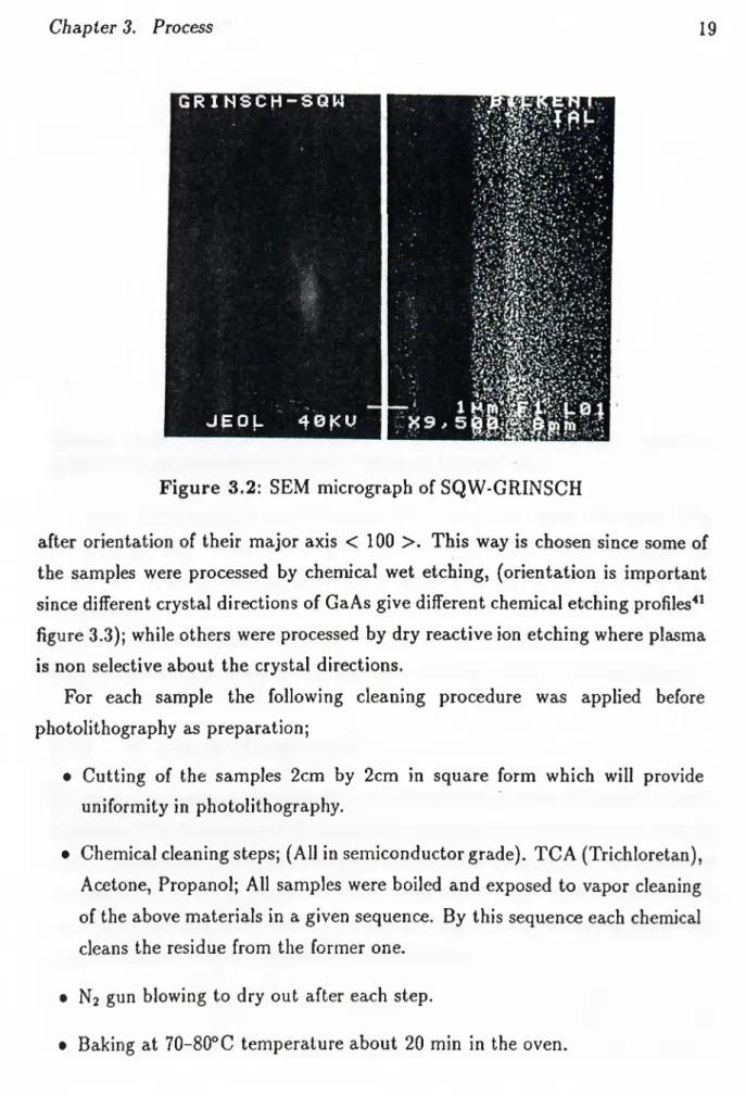
Chapter 3. Process 19
G R I N S C H - S Q W
J E O j - -^0|<M
F ig u re 3.2: SEM micrograph of SQW-GRINSCH
after orientation of their major axis < 100 >. This way is chosen since some of the samples were processed by chemical wet etching, (orientation is important since different crystal directions of GaAs give different chemical etching profiles^^ figure 3.3); while others were processed by dry reactive ion etching where plasma is non selective about the crystal directions.
For each sample the following cleaning procedure was applied before photolithography as preparation;
• Cutting of the samples 2cm by 2cm in square form which will provide uniformity in photolithography. •
• Chemical cleaning steps; (All in semiconductor grade). TCA (Trichloretan), Acetone, Propanol; All samples were boiled and exposed to vapor cleaning of the above materials in a given sequence. By this sequence each chemical cleans the residue from the former one.
• N2 gun blowing to dry out after each step.
Chapter 3. Process 20
CROSS SECTION
F ig u re 3.3: (100) oriented GaAs wafer illustrating cleavage planes and anisotropic as evidenced by a raised mesa and etched slots
Some of the samples were recleaned by wiping with these chemicals if their lithography step failed, and the process was repeated. In a very rare cases ultrasonic cleaning was applied in case of peeling off of the metalization was encountered.
The most important of all in the cleaning process is to follow a continuous process flow (i.e., without giving any long delays between the process steps).
3.3
Photolithography
In planar technology complex devices are obtained after successful steps in sequence. The beginning of these steps is covering the substrate by a radiation sensitive material called photo-resist while photolithography is patterning the required model on the photo-resist for subsequent steps. This is achieved by passing high energy radiation or UV-light through a mгısk containing the pattern and illuminating the photoresist covered substrate.
Chapter 3. Process 21 Mirror Hg Arc Lamp d - Condenser Lens Mask (4-10X) Of Chip
F ig u re 3.4: Schematic of refractive optics reduction projection printer. Main elements of photolithography can be summarized as follows^^ (fig ure 3.4).
• Source for exposition.
• Mask containing the required pattern.
• Different lenses and mirrors (Depending on the type of source). • Mechanical setups for precise aligning and adjustments.
• Photo-resist material.
Chapter 3. Process 22
Positive Resist
J1
Negative Resist
Unexposed Space Unexposed Space
F ig u re 3.5: Positive and Negative Photoresist behavior after the develop
3 .3 .1
P h o to r e s is ts
Photo-resists are classified into three different types as; positive photo-resists, negative photoresists and high radiation sensitive e-beam resists. In positive photo-resist applications, photo-resist areas which are exposed to radiation are removed from the substrate by a proper solvent called developer. While the process for the negative photo-resist is reverse of this procedure (figure 3.5).
Both types of photo-resists are suitable for reactive etching processes but only positive photo-resist handles the lift-off applications. Main idea behind the exposition is to change chemical structure of photo-resist material from one form to another (i.e., polar to nonpolar or polymer to monomer). Also by adding different chemicals to photo-resists their capabilities can be adjusted (contrast, speed , sticking coeff. etc.) see table below.
3 .3 .2
P r in tin g
Optical lithography depending on the distance between the mask and the substrate is divided into three types. If the distance is on the order of centimeters, it is called projection printing. For small separations of about few microns, it is called proximity printing and the last one is contact printing where mask touches the substrate.
In projection and proximity printing techniques resolution is weak compared to contact printing, but for repetitive printing (steppers) contact printing can not be used because it is always contiguous for the mask and substrate. For pilot productions contact printing is the most effective one since it gives the best light
Chapter 3. Process 23
F ig u re 3.6: Mercury lamp output for resist exposure. intensity distribution between the mask and the substrate.
W ith these techniques optical lithography uses different types of exposure sources which emit light in different spectral regions. One of the popular sources of optical lithography is Hg arc lamp and it has emission spectra in several strong lines. Some of the lines are 365 nm (I-line), 405 nm (G-line), 435 nm (G-line) Figure 3.6. Whereas Hg arc lamp has weak emission between 360-450 nm region and is replaced by other optical exposure sources.
3 .3 .3
E x p erim en ta l
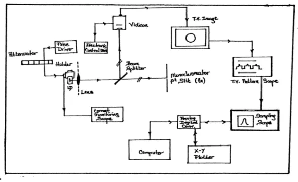
Comparing the cost of optical lithography with other techniques and since the fabrication is just for pilot production, optical exposition technique is preferred for laser diode fabrication. The device chosen for this purpose is a MJB-3 UV- 300 mask aligner (figure 3.7) which is equipped with a 300 watt Hg arc lamp and suitable optics for 320 nm wavelength from Karl-Suss. The device is capable of exposing in two different types of printing, contact and proximity with standard and high precision modes. The device was calibrated by a model 1000 UV power- meter on chuck exposition area with ±5% to continuous intensity mode at 12.5 mW/cm^.
Chapter 3. Process 24
F ig u re 3.7: Basic schematic of MJB-3 UV-300 Mask Aligner
value offers us contrast enhancing, compensation for standing waves and substrate reflectivity and extending the resolution as wavelength is inversely proportional to the energy of radiation.
Of course one of the main drawbacks of using shorter wavelengths is loss of depth of focus. Numerical aperture of a lens is given by NA,
N A = nsin(0) =
2
/
6 (View angle), f (Focal length), NA (Numerical aperture) n (index of refraction), D (lens diameter).
Resolution of a lens at Rayleigh limit for two opaque objects ; kX
W = NA
Chapter 3. Process 25
A (wavelength), k (material constant·*®) values are given in the table below.
k = 0.3 top surface image resists
0.5 multilayer resists
0.75 single layer resists
1.1 resists over reflective surfaces ( Al, Au)
Depth of focus (DF) of a lens for a determined wavelength A; A
DF = ±
2NA^
Because of the self aligning nature of the fabrication of laser structures in lAL laboratories only one lithography step weis applied in the whole process. Photoresist AZ 5214-E with AZ 400K developer were chosen for later lift-off
m
applications.
For spinning of the photo-resists, Model SM 120 spinner which is equipped with a photo-resist dispenser unit w<is used. Device is capable of blowing N2 before dispensing the photo-resist for final cleaning and has various speeds between 500-10.000 rpm and acceleration controls for two different settings. In baking steps temperature controlled Heraus-6030 oven was used.
The following lithography steps are applied during fabrication after cleaning of the samples,
• Spinner P a r t :
• Dispensing of the HMDS.
• Spinning at speed 1. 1000 rpm of 2 sec. • Spinning at speed 2. 5000 rpm of 10 sec.
Chapter 3. Process 26
• Filtering photo-resist at low pressures up to 0.2//m. • Dispensing of the photo-resist.
• Spinning at 1000 rpm. of about 10 sec. • Spinning at 5000 rpm. of about 40 sec.
• 1cm Prebaking at 85 C about 40 min in oven.
• Aligning and Mcisking :
• Mask containing 5fim and 12/xm stripes with separation of бООрт is used. • Samples are aligned along the major axis and exposed at CI2 mode: 12
mW/cm* for 38 seconds.
• Developing :
• Exposed samples are developed in AZ-400K -|- DI water solution (1:4) in contrast mode of developing. Developing was done in a dynamical way in a stirrer along the stripes.
• After developing, samples are rinsed in continuous flow of DI water. • Dry filtered Nj spraying.
Chapter 3. Process 27
3 .3 .4
P rocess notes
Reproduction of the image is influenced by many factors such as film thickness, prebake conditions, exposure conditions, developer parameters (i.e., concentration, agitation, temperature, developing time), surface topography and image geometries. Applying agitation which is known cis dynamical developing, increasing temperature, and increasing developing time yields big amounts of film losses from the surface in short times. W hat is required in our process was controlling the contrast of the photo-resist and obtaining the highest possible contrast in the stripe figures. In case of over-exposition and over developing for positive photoresist applications loss of photo-resist from the patterned figures is intolerable for the following dry etch steps. Above process steps are the optimum ones giving the best results.
Before application of photo-resist using one of the surface primers HMDS (Hexamethyldisilazane) is found to be beneficial. Application was done in pure form where also diluted and vapor phfise applications are taking place in lithography. To achieve proper adhesion properties, it is necessary for the resist and the substrate to have equal surface energy values. The surface energy of water is 72 dyne/cm*, the approximate energy value of photo-resist is 32-35 dyne/cm^ and surface energy of an HMDS treated surface^® is 4.6-16 dyne/cm^. Since HMDS is hydrophylic in nature, resist must be applied immediately afterwards onto the treated surface. Vacuum is best for this purpose. Removing water from the surface by dehydration is also very important. When no HMDS is used a physisorption condition exists. In case of long delays between dehydration and resist applications lifting of the photoresist in further steps can be seen. With priming agent aging is also seen by chemically adsorption of water (chemisorption) but it is much more slower.
Chapter 3. Process 28
'TIOwalBTBKSi
Figure 3.8: Basic schematic of RIE
3.4
Reactive Ion Etching (RIE)
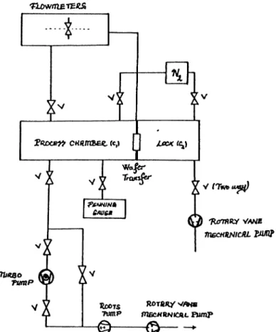
Asymmetric parallel reactor usage at low pressures in plasma etching is usually called as reactive ion etching (RIE). The term "diode reactor” has also been used to refer to reactors of such kind. Before giving the detailed information on RIE, mechanism of plasma etching may be helpful. A simple plasma reactor consists of opposing parallel plate electrodes in a chamber that can be maintained at low pressure, ranging from 0.01 to 1 Torr figure 3.8. When a high-frequency voltage is applied between the electrodes, current flows through the gas mixture, forming a plasma that emits a characteristic glow. Light emitted at this moment is the characteristic of plasma and material inside. It can be used in in-situ monitoring processes.
Chapter 3. Process 29
Neutral and charged species exposes the material at the lower electrode surface. Some of these species react with the substrate and form volatile products which evaporate hence etching the substrate. In such plasmas ionization rates are very small; one charged particle per neutral atom and molecule densities leading to 10®-10"cm“^, Positive charge is mostly singly ionized atoms and negative are the free electrons. Main carriers are the electrons since they are light and mobile. Neutral gas remains at normal temperatures while electrons gain tens of thousands of Kelvin from the applied field. Because electron mass is almost 0.0005 times that of other species, main contribution of cooling the plasma comes from the heat transfer between the plasma gas and the chamber walls. Elevated electron temperature permits electron molecule collisions to excite high-temperature reactions that form free radicals.
Plasma etching is characterized according to rate, anisotropy, selectivity, the degree of loading effect and texture (surface roughness) on the surface of the samples.
By convention, the term anisotropic etching refers to preferential erosion in a direction normal to the surface of the wafer. Selectivity is the ratio of etching rates between two different materials immersed in the same plasma, for example, GaAs and Al^Gai.^As. Loading is a term used to describe a measurable depletion of active etchant species from the gas phase brought about by the consumption of this reactant in the etching process.
In principle the plasma etchant feed gas is chosen with required selectivity over processed materials and minimization of any loading effect and to avoid excessive surface texturing and polymer deposition. Anisotropy degree becomes important in etching of 3-5/xm patterns. Some of the etching profiles are given in (figure 3.9).
Isotropic etching has no preferential direction. This leads to isotropic circular profiles which undercut a mask. Overetching increcises the undercut and radius eventually making sidewalls nearly vertical. In anisotropic etching, the sheath field makes ions strike horizontally and ion assisted chemistry forms profiles with vertical sidewalls that line-up with the edges of the mcisk. Anisotropy is
Chapter 3. Process 30 W(\UUM MASK S U B ST R A T E 1 S U B ST R A T E 2 I I [yrrr _<Jv IS O T R O P IC
1
O V ER ET C H\
GX5SnS53 ANISOTRO PICF ig u re 3.9: Isotropic(left) and anisotropic etching(right)
useful to get fine figures in micron range. While isotropy is helpful for stripping of photoresist, etching large figures and removing of oxidation m<isks in an economical way. Isotropic etchants often exhibit a loading effect that results from etchant depletion in the gas phase caused by reaction with the substrate material. If a significant portion of the re<ictive etchant species is consumed in etching reactions, their concentration will decrease rapidly with the area of etchable material in the reactor. Use of a large reactor volume with high surface area will minimize the sensitivity of etch-rate to the area of etchable material. If more than one species participate in etching, like in fluorine based plasmas where Cl and F atoms individually helps etching, each shows its own loading effect. Concentration of fluorine atoms etching GaAs in a plasma is usually limited by reaction with substrate, giving loading effect. Chlorine atom concentrations in chlorine containing plasmas tend to recombine rather than etching reaction. Chlorine plasmas is commonly insensitive to load size and feature topology and ion bombardment determine the etching rate and nature. One can use them as a good drilling machine in micro-fabrication applications.
Chapter 3. Process 31
LOWER ELECTRODE ANO
WAFER PLATEN
-UPPER ELECTRODE WAFERS
PTREX CYLINDER
GAS RING
ETCH GAS-> PUMP
F ig u re 3.10: A parallel-plate "Reinberg” style reactor with radial gas flow. In RIE reactors, wafers are placed on the smaller bottom electrode. Parallel plates are highly asymmetric and the external circuit has a blocking capacitor so th at smaller electrode develops a negative D.C. bias superimposed on the applied RF signal (figure 3.10).
The high potential RF power lead is usually connected to smaller electrode, with the larger electrode grounded at common potential. This is necessary to maintain a large area ratio since there are usually grounded surfaces elsewhere, in and out of the reactor chamber. These areas are capacitively coupled to the plasma and therefore increase the effective area of grounded electrode. In controlling the etching, instrumental parameters or discharge variables are used instead of theoretical models. Among them radio frequency(RF) input power, reactor pressure, RF excitation frequency, temperature, flow rate, feed gas composition, reactor geometry and material of construction have the great importance. Choosing one of these parameters and fixing the others is the way to study the effect of over etching.
Pressure directly influences major phenomena that control plasma etching. As pressure is lowered below about 0.1 torr the characteristic potentials across the sheaths and voltage applied to a discharge rise sharply in the range of hundred volts to 1000 volts. As this happens mean free paths of the species also increase so the larger sheath potential induces a corresponding increase in the energy of ions bombarding substrate surfaces. Sputtering doesn’t take plaice until ion
Chapter 3. Process 32
F ig u re 3.11: Dependence of U,6 on RF power (RIE) for Oj and CCI2F2; P=0.8 Pa
bombardment energy exceeds a material and ion specific threshold.^^ Sputtering efficiency is defined as atoms removed per incident ion and this increases beyond threshold and usually stays well below unity. Since low pressure favors higher ion bombardment energies it also favors etching by the energy driven damage mechanisms. However ion energies far above the threshold are undesirable because selectivity ratios decrease with increasing ion energy and because there may be induced damages to devices.
CCI2F2 is a well known selective etchant of GaAs on Al,Gai_j;As. Because of this reason it is used for fabrication of modulation doped FET’s and other heterojunction devices. During the etching of GaAs, volatile AsFxCly and GaCb products are formed until a barrier layer is created when the GaAs/Al^Gai.^As interface is reached. The barrier layer consists of AIF3 and GaCUFy. This surface layer prevents the etching of aluminum alloys at intermediate pressures (30 mtorrs). CCI2F2 selectively etches GaAs up to 1000 times faster than AlxGai_xAs. Unsaturated CCUFy species can form thin side-wall films, which simulate anisotropic etching by ion bombardment.
Chapter 3. Process 33
In RIE at low pressures (few mtorrs) at high self bias (SB) voltages GaAs in CCI2F2 shows acceptable anisotropy and etching-rate. At high pressure the unsaturated species can be adsorbed at the surface and polymerize (forrrung thick polymer film). The growth of the polymer film incretises with partial pressure of the unsaturated CClrFy species. This polymer formation completely stops the etching (mostly in Al^Gai.^As etching galliumtrifluoride is dominant and involatile).
In laser diode structures, to etch ridge-waveguides freon-12 (CCI2F2) was chosen as process gas. Machine used for this purpose is a parallel plate Leybold LEl-301 reactive ion etcher operating at 13.56 MHz RF voltage. Chamber pressure can be lowered by turbo pumping down to few millibars. Water cooled lower electrode gives the ability to suppress the thermally activated reactions. By this means only energy driven, ion assisted etching reactions, that give anisotropic profiles, can occur. Choosing pressure at 0.4 Pa gave us decrease of selectivity between one third, to one fourth. Self bias voltage was seen around 350 V with 54 W actual RF power (figure 3.11). In GRINSCH structure material thickness th at must be etched was calculated as 0.7fim in capping layers. Etching was stopped 0.4/im away from the layers where grading begins. Taking into account that anodic oxide will also consume from the surface about 0.1/im, stopping OApm away froni graded layers helps the confinement of lateral modes inside the waveguide. Etching was performed at two steps. In the first step, sample was etched up to 5200
A
from the surface with the parameters:First Step:
Etching gas : CCI2F2 ( Freon 12 ) Flow : 4 seem.
Pressure : 0.4 Pa
Power RF : 46 W ( at 13.56 MHz.) Self bias voltage : 322 Volts
Chapter 3. Process 34 IB T"5 S c a n : 150um S u e e d : Low F o r e « : 5 __ ---E : · / i \ / \ 12 lO 8 6 4 2 O xlOOO P r o9 ramm i n g x C u r s o r s : A v g m = 1 3 , 1 6 3 A .«\/e r x /A H o r i z /u m M: 1 3 . 1 3 0 0 1 1 O Ri 1 3 , 1 4 6 0 1 1 O A : - 1 6 O Re s o l u t i o n : Low S г a г u s : — f _ /
/
\
/
\
/
\
/ 12 10 8 6 4 2 P r o g ra m m in g: C u r s o r s : A vg H t « 1 3 .1 2 0 A *v/e r t / A H o r i z/u m M: 1 3 , 0 3 7 0 9 5 R : 1 2 , 9 9 3 0 8 9 4 4 5 P e s o 1u t I o n : Low S t a t u s : R e v . 5 . 2 / 5 . 3 / F 5 . 0 1 0 : 4 9 0 8 / 1 1 / 9 3 ID : O S c a n : lOOum S o e e d : Low Fo r c e : 5 R e v . 5 . 2 / 5 . 3 / F 5 . 0 1 0 : 4 6 0 8 / 1 1 / 9 3 S l o a n DEKTAK 3 0 3 0 S T/
\
\
/
\
. -/
\
J 8 1 ^ 8 3 8 4 ^ 8 6 8 7 ^ 5 0 0 4 0 0 3 0 0 200 lOO O x lO P r o g ramm i n g : C u r s o r s ; A v g H t * 5 1 4 5 A r t / A H o r i z /u m M: 5 1 6 9 0 8 4 . 6 R : 5 1 2 4 0 8 2 . 3 L · ! 4 5 1 . 7 R e s o 1u t i o n ; Low S t a t - u s : 5 . 2 / 5 . 3 / F 5 . 0 1 1 : 1 9 0 8 / 1 1 / 9 3F ig u re 3.12: Profiles of the 5pm and \2pm stripes: (a) Before etching (b) After first etching step.
Dummy samples run in the same process was taken out and after stripping of the photoresist, etch rate was calculated from the DekTak stylus profilometer reading, (figure 3.12).
Chapter 3. Process 35
T5 T"o
S c a n : lOOum S o e e d : Low F o r c e ! S _______
F ig u re 3.13: Etching profiles of the 5/im and 12pm stripes after second etching step.
Depending on the data obtained from the first step second etching step was performed and same Dektak measurement was done on the dummy sample. After second run, etching depth reached around 7050 Awhich is exactly the required etching thickness, (figure 3.13). Second Step :
Etching gas : CCI2F2 ( Freon 12 ) Gas Flow : 4 seem.
Pressure : 0.4 Pa
Power RF : 46 W (at 13.56 MHz.) Self bias voltage : 345 Volts
Etching time : 5 min. CI2/BCI3 gais mixtures can also be used instead of the CCI2F2 plasma. Since this gas mixture doesn’t show any selectivity ( 1:1) between AlxGai_iAs and GaAs and etches them at high rates, up to 4500 (A)/min (U,i,=200 V, P=0.8 Pa, Flow=6 seem) which lowers the process times. Previous studies^* of GaAs RIE in CI2 and BCI3 plasma was showing 1.5 times less damage
Chapter 3. Process 36
on surface of GaAs in Raman scattering spectrum. Of course small surface damages on GaAs or AlrGai_*As can somehow be healed in further annealings a t metalization step.
3.5
Anodic Oxidation
In stripe geometry laser diode devices, to decrease the injected current and to restrict it into a region one must insulate all the areas, except the current path on top of the stripe. There are several ways to achieve this. One of them, possibly the easiest, is to apply anodic oxidation to the p-type region.
In our lasers we also chose anodic oxidation . Nature of our process yields self aligning of anodic oxidation area along the stripe, since only the arecis that could pass the current through solution are oxidized. Laser structures in the stripe-up position was used as anode and P t was used as cathode. Cathode Pt was dipped into the anodic oxidation solution while laser structure was held by soft vacuum and placed in touching position to the surface of the solution figure 3.14. After aligning the cathode and anode positions 100 V D.C. was applied to the structure until current dropped to zero. This is the result of self stopping nature of the anodic oxide growth. For successive applications, anodic oxide growth rate for different structures was found as 21
A
per volt in this solution. Applying 100 volts gives us approximately 0.2/im anodic oxide thickness, dark blue going to purple in color due to interference.Anodic oxidation solution:
At the first stage 3 gr Citric Acid was mixed with 97 ml DI water. In this way liquid citric acid solution was obtained. This solution is further mixed by 194 ml Etylen Glycol. NH4OH was added to obtain the final solution until its PH value reads 6.5 .
Chapter 3. Process 37
F ig u re 3.14: Anodic oxidation setup.
3 .5 .1
P r o c e ss n o tes
Before anodic oxidation was applied, samples were dipped into the dilute HCl (6-8 %) solution a few seconds. Since HCl is one of the etchants of the GaAs and AlxGai_j;As, it helps to get more smooth and clean surfaces, it is essential for anodic oxide sticking. This way of cleaning is not advised for high A1 concentration layers since Al^Gai-^As etching rate is higher than the GaAs in HCl. It may give nonuniform surfaces at the end of acid application. Similar behaviour were observed in the anodic oxidation process for high A1 concentration structures. If applied current is set above few tens of a mA even though the oxidation ends fast, some of the areas were found not to be oxidized, while some oxidations areas goes deeper in such structures. In extreme cases these deeply oxidized areas may combine and can penetrate to the stripe, resulting in a loosening of the chip (figure 3.15).
In all of the applications when oxide is grown on the surface of the chip, it was taken out from the solution and dipped and washed in DI water to get rid of any kind of oxidation solution. Following this step chips were dried by dry-Nj spray and baked at 55°C about 3 minutes. Putting the chip just at the surface of oxidation solution is essential since any wetting will result oxidation
Chapter 3. Process 38
F ig u re 3.15: Oxide etching characteristic of HCL
of the n-side which is intolerable. Chemical reaction is sensitive to heat and agitation. Agitation mechanically may cause stripping the oxide from some areas while exposition to high intensity light speeds up the oxidation. All the laser structures were excited by light during the anodic oxidation step.
For cases where anodic oxide grew nonuniformly, etching half the thickness of the oxide by the above cleaning method in dilute HCl and regrowing it to again up to 0.2/im can be proposed (figure 3.15). Like in all oxidation processes anodic oxide also grows into the material and the thing that must be taken into account here is to allow enough thickness of capping layers for this extra step in RIE.
GaAs native oxide which is mainly composed of gallium-trioxide and arsenic- trioxide is known to be an unstable oxide. Because of this deficiency it can not insulate the laser structures at high current pumping rates (giving high leakage currents) putting another insulating layer (noncrytalline SiO*) by PECVD was found beneficial.