Armchair nanoribbons of silicon and germanium honeycomb structures
S. Cahangirov,1M. Topsakal,1and S. Ciraci1,2,*
1UNAM–Institute of Materials Science and Nanotechnology, Bilkent University, Ankara 06800, Turkey 2Department of Physics, Bilkent University, Ankara 06800, Turkey
共Received 25 January 2010; revised manuscript received 6 May 2010; published 25 May 2010兲 We present a first-principles study of bare and hydrogen passivated armchair nanoribbons of the puckered single layer honeycomb structures of silicon and germanium. Our study includes optimization of atomic structure, stability analysis based on the calculation of phonon dispersions, electronic structure, and the varia-tion in band gap with the width of the ribbon. The band gaps of silicon and germanium nanoribbons exhibit family behavior similar to those of graphene nanoribbons. The edges of bare nanoribbons are sharply recon-structed, which can be eliminated by the hydrogen termination of dangling bonds at the edges. Periodic modulation of the nanoribbon width results in a superlattice structure which can act as a multiple quantum well. Specific electronic states are confined in these wells. Confinement trends are qualitatively explained by including the effects of the interface. In order to investigate wide and long superlattice structures we also performed empirical tight-binding calculations with parameters determined from ab initio calculations. DOI:10.1103/PhysRevB.81.195120 PACS number共s兲: 73.22.⫺f, 63.22.⫺m, 61.48.De
I. INTRODUCTION
Graphene, a two-dimensional 共2D兲 honeycomb structure of single layer of carbon atoms, has been synthesized and established as a material with wide range of unusual properties.1–3 It is a semimetal with a band profile having linear dispersion near the Fermi level,4which attributes to its electrons a massless Dirac fermion behavior. Quasi-one-dimensional 共1D兲 derivatives of graphene, called graphene nanoribbons, were also produced recently.5,6Graphene nan-oribbons are semiconductors having interesting electronic properties depending on their geometry. These properties can be used to fabricate nanodevices as field effect transistors, spin valves, multiple quantum wells, etc.7–11
2D honeycomb structures and 1D nanotubes of Si and Ge were studied earlier.12,13 Stringent stability tests have re-cently shown that 2D honeycomb structures of Si and Ge can be found stable in a slightly buckled geometry.14These struc-tures have similar properties as graphene and thus carry the potential of being used in the similar applications.15 Com-pared to graphene, the interatomic distance is larger in Si and Ge, so the diminished-overlaps cannot maintain the pla-nar stability anymore. Eventually, the sp2hybrid orbitals are slightly dehybridized to form sp3-like orbitals, which in turn results in a puckered structure.16 Freestanding graphene sheets and nanoribbons can be produced spontaneously, but it is not the case for 2D honeycomb structures of Si共silicene兲 and Ge. However, there are plenty experimental work on growth of Si nanoribbons especially on Ag surface.17,18 These highly metallic nanoribbons are formed by self-organization and have straight, atomically perfect, and mas-sively parallel structures.18The electronic structure of Si na-noribbons on Ag surface was also investigated theoretically.19
This paper reveals the atomic and electronic structure of armchair Si and Ge nanoribbons. Stability analysis, based on the calculation of the phonon dispersions via the force con-stant method, was performed. Energy band structure calcu-lated by first-principles density-functional theory共DFT兲 was
used to generate the parameters of the tight-binding model. It is found that armchair nanoribbons of Si and Ge are stable and their band gap vary with their width displaying a family behavior.20,21 Formation of multiple quantum well structure in superlattices consisting of periodically repeated junctions of nanoribbons having different widths was also investigated in detail. A 1D model was proposed to understand the effect of the interface in superlattice structures. It is found that specific electronic states are confined in these superlattice structures. The interface effects, which can explain unex-pected confinements, are revealed.
II. METHODS
We have performed first-principles plane-wave calcula-tions within local density approximation 共LDA兲 共Ref. 22兲 using projector augmented wave 共PAW兲 potentials.23 All structures are treated within supercell geometry using the periodic boundary conditions. A plane-wave basis set with kinetic energy cutoff of 300 eV is used. In the self-consistent potential and total energy calculations, the Brillouin zone 共BZ兲 is sampled by 共15⫻1⫻1兲 special k points. All atomic positions and lattice constants are optimized by minimization of the total energy and atomic forces. The vacuum separation between the nanoribbons in the adjacent unit cells is taken to be at least 10 Å. The convergence for energy is chosen as 10−5 eV between two steps, and the maximum Hellmann-Feynman forces acting on each atom is less than 0.02 eV/Å upon ionic relaxation. Numerical plane-wave calculations have been performed by using VASP package.24,25 Phonon dispersions were obtained using the force constant method with forces calculated in a 共5⫻1⫻1兲 supercell.26,27 Cou-pling parameters of empirical tight-binding calculations are determined from the ab initio results and are used to treat wide and long superlattice structures, comprising as many as 3600 Si atoms.
III. ATOMIC STRUCTURE AND STABILITY
We first investigate the atomic structure of bare and hy-drogen saturated armchair nanoribbons of Si and Ge. The
ideal honeycomb structure is cut parallel to the nearest-neighbor bonds to form an ideal bare nanoribbon with a cer-tain width. Armchair nanoribbons are classified by counting the number, n, of Si 共or Ge兲 atoms forming a zigzag chain perpendicular to the cut direction. Accordingly, there are 2n Si 共or Ge兲 atoms in the primitive unit cell of an ideal bare armchair nanoribbon. This structure is treated by a supercell having periodic boundary condition in cut direction and a vacuum spacing in other directions. To lift the constraints imposed by共1⫻1兲 unit cell, we have used 共2⫻1兲 supercell. Figure 1共a兲 presents the atomic structure of a sample bare armchair Si nanoribbon after structural relaxation. Here one can see a共2⫻1兲 reconstruction at the edges, which would be missed if 共1⫻1兲 unit cell was used in the calculation. The edge reconstruction is reminiscent of the reconstruction of Si共100兲-共2⫻1兲 surface. In the latter case, two adjacent sur-face Si atoms each having two sp3-dangling bonds come closer and form a new dimer bond using one sp3-dangling bond from each atom. At the end, the number of sp3dangling bonds is halved and hence the energy is lowered through reconstruction. Similarly, in Fig. 1共a兲A and B atoms come closer to form a bond. Since the nature of bonding is modi-fied around B atom, the ABC triangle is bowed. At the end, the number of the sp2 dangling bonds is halved. Note that this kind of reconstruction is not seen in bare armchair graphene nanoribbons. Moreover, in graphene and its nanor-ibbons all atoms lie in the same plane, while structures con-sidered here are slightly buckled. The separation between adjacent atoms in the perpendicular direction to the plane is around 0.4 and 0.6 Å for Si and Ge nanoribbons, respec-tively.
Figure1共b兲presents the atomic structure and bond-length distribution of a sample hydrogen saturated armchair silicon nanoribbons. In contrast to bare nanoribbons, saturation by hydrogen lifts the共2⫻1兲 reconstruction at the edges. In Fig. 1共b兲 there are n = 9 Si atoms forming zigzag chain perpen-dicular to the nanoribbon axis and hence this armchair nan-oribbon is classified as ASiNR-9. Accordingly the number of Si共or Ge兲 atoms in the primitive unit cell is 2n. Note that the bond-length distribution is nearly uniform except a sudden decrease at the edges. This pattern was also observed in arm-chair graphene nanoribbons.20
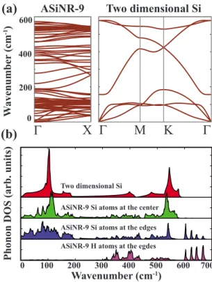
Figure2共a兲presents the phonon dispersion profile for hy-drogen saturated ASiNR-9. Also phonon dispersion profile of 2D silicon, reproduced from Ref. 14, was shown for com-parison. It is not possible to generate the dispersion profile of ASiNR by folding that of 2D Si, but the pattern is similar to that found in nanotube dispersion profiles obtained by zonefolding.28In the phonon dispersion profile of hydrogen saturated ASiNR-9 all modes are real, except for some small imaginary frequencies calculated for the twisting acoustic mode, TW, near the⌫ point. This issue was faced earlier and was attributed to the limitations of the computational precision.29 Thus, the structure is predicted to be stable. Computational cost of this calculation is very high, so we were not able to calculate the phonon dispersions for other ribbons. Nevertheless, all ASiNRs have very similar atomic configuration, and thus they are also expected to be stable. The phonon dispersion profile of 2D Ge is similar to that of Si.16 But in Ge structure the acoustic and optic modes are well separated. Also due to softer bonds the wave numbers of Ge structure is halved compared to Si. Thus AGeNRs are also expected to be stable, while exhibiting the mentioned differences.
Phonon densities of states 共DOSs兲 of hydrogen saturated ASiNR-9 projected to atoms at different locations in the na-noribbon are presented in Fig. 2共b兲. Shown is also DOS of the 2D Si honeycomb structure in the same figure. DOS pro-jected on Si atoms at the center of the nanoribbon is very similar to that of the 2D Si. As the width of the nanoribbon (a) Bare (b)H passivated Bond Length (Å)
2.2 2.3 2.4 Si Ge n=9 A B C
FIG. 1. 共Color online兲 共a兲 Atomic structure of fully relaxed bare armchair Si nanoribbon of width n = 9共ASiNR-9兲. 共b兲 Atomic struc-ture and bond-length distribution of hydrogen saturated ASiNR-9. Similar pattern is observed in hydrogen saturated AGeNR-9. The primitive unit cell of ASiNR-9 is shaded. The zigzag chain of Si atoms perpendicular to the nanoribbon axis is delineated by the dashed lines.
(a)
W avenumber (cm -1) 0 200 400 600ASiNR-9
Two dimensional Si
Γ
X
Γ
Μ
Κ
Γ
0 100 200 300 400 500 600 700
Wavenumber (cm-1)
Two dimensional Si
ASiNR-9 Si atoms at the center ASiNR-9 Si atoms at the edges ASiNR-9 H atoms at the egdes
Phonon
DOS
(arb.
units)
(b)
FIG. 2. 共Color online兲 共a兲 Phonon dispersions calculated for hydrogen saturated ASiNR-9 and for 2D honeycomb structure of Si. States that appear above 600 cm−1 are related to Si-H bonds of hydrogen saturated ASiNR-9 and were not shown. 共b兲 Phonon DOSs of the hydrogen saturated ASiNR-9 projected to Si atoms at the center and at the edges and also to H atoms at the edges. DOS of 2D honeycomb structure of Si is also presented for comparison.
increases, this similarity is expected to be enhanced. How-ever, DOS projected on Si atoms at the edges deviate from that corresponding to 2D Si. Especially, four optical peaks above 600 cm−1 are clearly originating from Si-H bonds at the edges. Also modes originating from short Si-Si bonds at the edges cause changes in DOS below 600 cm−1.
IV. ELECTRONIC STRUCTURE
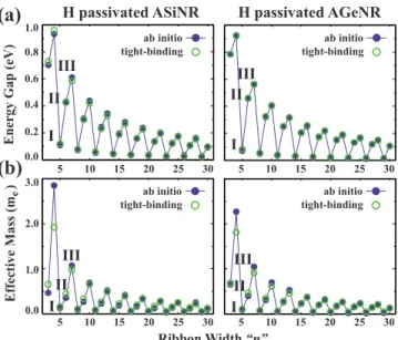
In this section, we investigate the electronic structure of hydrogen saturated Si and Ge nanoribbons. Nanoribbons having widths from n = 3 to 30 were investigated. Figure 3 presents the variation in energy gaps and effective masses with the ribbon width given in terms of n. Band gaps are direct and located at the⌫. One can see three branches with decaying profiles originating from the quantum size effect. Here in ascending order of the band gaps, we would like to name these branches with widths n = 3k + 2, 3k, and 3k + 1 as family I, II, and III, respectively, where k is an integer. This “family behavior” was also observed in armchair graphene nanoribbons.20This trend is explained by foldings of infinite graphene band profile, which is easily understood by using a tight-binding model. The simplest possible model is to as-sume that only the first nearest-neighbors interact and have equal hopping parameters with self-energies set to zero. But this model results in zero band gap for the members of the family I. Fortunately, this problem is fixed if a different pa-rameter is used at the edges.20As we mentioned in the pre-vious section, the Si-Si 共and Ge-Ge兲 bond length is appar-ently smaller at the edges, which implies that edge bonds are stronger. That is why defining a different hopping parameter
at the edges reflects the nature of the system better. Accord-ingly, we set the nearest-neighbor hoping integrals to be t共1+␦兲 at the edges and t otherwise. In our model all self energies were set to zero. The tight-binding parameters were obtained by fitting to the first principles results. Results pre-sented in Fig.3共a兲show that the model used here is success-ful in reproducing the DFT band-gap trends of both Si and Ge armchair nanoribbons. Since we did not make GW cor-rection to the band gaps, the nearest-neighbor hopping inte-grals, which are found to be t = 1.03 eV for Si and t = 1.05 eV for Ge, are expected to have larger values and should be taken as a qualitative result. However, the relative increase in the hopping integrals at the edges defined by ␦ can be taken as a quantitative result. We have found ␦ = 0.12 and␦= 0.08 for Si and Ge, respectively. Interestingly, the value found for Si is equal to that of reported value for the armchair graphene nanoribbons. To sum up, the tight-binding parameters determined for Si and Ge armchair nan-oribbons are tSi= 1.03 eV, tGe= 1.05 eV, tSi,edge= 1.15 eV, and tGe,edge= 1.13 eV.
Figure3共b兲presents the effective masses of the first con-duction band calculated by using the formula
mⴱ=ប2
冉
2E共k兲k2
冊
−1, 共1兲
where E共k兲 is calculated by using both DFT and tight-binding model mentioned above. Note that parameters of the tight-binding model are generated by using only the band-gap information at the ⌫ point, but it can reproduce the second-order momentum derivative and thus the effective mass, which is in agreement with that of ab initio calcula-tion. The deviation from this agreement is seen in the ulti-mately thin nanoribbons. This is because, in these nanorib-bons the edges affect the rest of the structure and the tight-binding model cannot be applied with the same success. Note that, the effective mass trends are similar to the band-gap trends and show the family behavior. Similar trends in the effective mass were also observed in the armchair graphene nanoribbons.30
V. SUPERLATTICES
In this section we investigate the electronic structure of superlattices formed by periodic junction of ASiNRs which have different widths. The variation in energy gaps with the ribbon width causes these structures act as a multiple quan-tum well and is expected to lead to interesting device appli-cations. In the past, superlattices of 2D GaAs-AlAs or Si-Ge heterostructures have been extensively studied to realize new generation electronic devices. Recently, superlattices of graphene have been synthesized experimentally.31The trans-port characteristics and electron confinement have been revealed.32 Here superlattices are formed by the junction of two different nanoribbons. In this study the lengths of con-stituent nanoribbons are taken to be equal. The unequal cases were studied for armchair nanoribbons of graphene.11We let l unit cell of a ribbon with the width of n1to make a perfect junction with l unit cell of a ribbon with the width of n2; once joined these structures form a supercell having the
1.0 0.0 0.2 0.4 0.6 0.8 tight-binding ab initio Energy Gap (eV) Ribbon Width“n”
H passivated ASiNR H passivated AGeNR
tight-binding ab initio 0.0 1.0 2.0 3.0 Effective Mass (m ) e 5 10 15 20 25 30 5 10 15 20 25 30 5 10 15 20 25 30 5 10 15 20 25 30 tight-binding ab initio tight-binding ab initio
(a)
(b)
I II III I II III I II III I II IIIFIG. 3. 共Color online兲 Calculated 共a兲 energy gap and 共b兲 effec-tive mass versus ribbon width, n, for hydrogen saturated Si and Ge armchair nanoribbons. Filled circles indicate the ab initio results while empty circles stand for the results of the tight-binding fitting. The fitting is performed using only the energy gap data. Parameters found from this fitting were used to generate the tight-binding ef-fective mass data. In each panel three branches are observed and named in increasing order of band gaps and effective masses as families I, II, and III.
length of 2l. Here n1and n2are chosen to be odd so that the ribbons are joined symmetrically. Then the resulting struc-ture is relaxed and the lattice constant of the whole strucstruc-ture is determined. This superlattice structure is labeled by its dimensions as SL共n1, n2; l兲. The indices 1 and 2 are arranged in a way that a ribbon with a width n1 has smaller band gap than a ribbon with a width n2. The width difference ⌬N = n1− n2is defined for classification purpose.
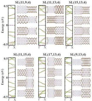
Figure4presents the band structure and projected charge density isosurface plots for sample superlattices having ⌬N = 2 and 4 calculated by DFT. The band profile is nearly sym-metric around the Fermi level and one can easily track the bonding and antibonding states from the charge density pro-file. As seen in the charge density plots, the band edge states of SL共11,9;4兲 and SL共11,13;4兲 superlattices are confined in the wide and narrow part, respectively. This can be explained by taking into account the band gaps of constituent ribbons of superlattice structures. Due to the symmetry between va-lence and conduction band edges of the constituent ribbons, the superlattice band lineup is always normal. As a result, the part having lower gap acts as a quantum well for electrons and holes. That is why, the electrons of SL共11,9;4兲 and SL共11,13;4兲 structures are confined in the n=11 part, which for both superlattices is the part having the smaller energy gap.
The situation is also similar for the structures having ⌬N=4. Electrons of SL共17,13;4兲 and SL共11,15;4兲 are
con-fined, respectively, in the wide and narrow part, which has the lower energy gap. Moreover, the superlattices con-structed by the nanoribbons, which are members of the same family, have similar electronic structure. In Fig.4the super-lattices having such common property are shown in the same column. Here one can see the similarity in the energy band profile of these structures. Another way to construct such structures is to increase the width of both constituent parts by n = 6k. To verify this, we have calculated the electronic struc-ture of SL共17,15;4兲 and SL共17,19;4兲, which yielded in the similar results as that of SL共11,9;4兲 and SL共11,13;4兲, except that in former structures the confinements are less pro-nounced because the band-gap difference is lower.
We have to mention that, even though the structures SL共9,13;4兲 and SL共15,13;4兲 have a considerable band-gap difference between constituent parts, they do not have con-finement neither in the wide nor in the narrow part. This is related to the interface effects, which will be discussed in a frame of another simple model.
Calculations for larger structures with ab initio techniques are computationally too expensive. So we have used the tight-binding model mentioned before. In Fig.4 one can see that the tight-binding model can reproduce the band edge profiles over the whole Brillouin zone. Moreover, the mag-nitudes of the eigenstates calculated by tight-binding model 共not presented here mimics the projected charge density pro-file of a given state. To get a qualitative picture of how the large structures behave, the tight-binding model was used.
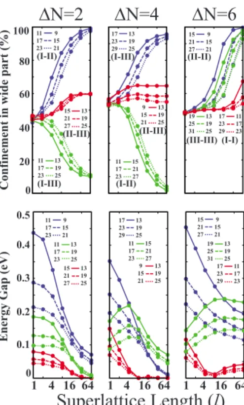
Figure5 presents the energy gap and the band edge con-finement strength trends generated by the tight-binding model for the superlattices having n = 9 – 31, ⌬N=2–6, and l = 1 – 64. The magnitude squares, 兩⌿兩2, of conduction and valence band edge eigenfunctions generated by the tight-binding model are equal. The confinement percentage in the narrow 共wide兲 part is defined as the sum of the magnitude squares of band edge eigenfunctions in the narrow 共wide兲 part multiplied by 100%, noting that the overall sum of the magnitude squares is normalized to 1. In Fig.5we see that, in agreement with the ab initio results presented in Fig.4, the band edge states are confined in the narrow part for SL共11,15;l兲 and SL共11,13;l兲 structures and in the wide part for SL共11,9;l兲 and SL共17,13;l兲 structures. These confine-ments are enhanced as the lengths l of the segconfine-ments increase because the strength of the well and the barrier increase. The trends shown in Fig. 5 also confirm the statement that the superlattices composed of the nanoribbons from the same family behave similarly. For comparison, in each panel of the Fig. 5 structures having such similarity are shown in the same style. Also the corresponding family names are pre-sented under the figure labels. The similarity can be seen in both confinement and the energy gap trends. For structures having ⌬N=6, the band edge states are always confined at the wide part. This is because the band gap for structures having⌬N=6 is lower in the wide part, so the wide part acts as a quantum well.
In Fig.5, one can see that there is no strong confinement in the wide or narrow part of SL共9,13;l兲 and SL共15,13;l兲 structures. This is also seen in the ab initio results presented in Fig.4. Moreover, the case is also true for the superlattices composed of the nanoribbons from the same family.
Never-Γ X Γ X Γ X Γ X Γ X Γ X 0 0.5 -0.5 0 0.5 -0.5 Energy (eV ) Energy (eV) SL(11,9;4) SL(11,13;4) SL(15,13;4) SL(11,15;4) SL(17,13;4) SL(9,13;4)
FIG. 4. 共Color online兲 Band structure and charge density isos-urface profiles for several superlattice structures. Solid共green兲 and dashed共red兲 lines stand for the ab initio and tight-binding calcula-tion results, respectively. Structures are labeled, as defined in the text, and are given on top of each structure. Top and bottom panels present the results for superlattice structures with ⌬N=2 and 4, respectively. Constituent nanoribbons of superlattices that appear in the same column are members of the same family. Charge density isosurfaces calculated by ab initio technique around the⌫ point for two conduction and two valence band edge states are ordered in the similar manner as they appear on the energy band structure.
theless, this cannot be explained by the band-gap difference of the constituent nanoribbons because there are superlattices composed of the nanoribbons having similar band-gap differ-ence but show strong confinement patterns. Actually, plotting the linear charge density of former structures along the peri-odic direction results in decaying profiles in both narrow and wide parts. Thus for these structures, the band edge states are localized at the interfaces. This means that the interface acts as a quantum well in these structures.
To consolidate the effects of the interface, we have to make an estimation about its effective energy gap and mass. For this purpose, we have chosen the energy gap and the effective mass of SL共n1, n2; 1兲 structure to represent the ef-fect of the interface between the nanoribbons with widths n1 and n2. This information was used in construction of a very simple 1D model, which qualitatively explains the confine-ment trends confine-mentioned so far. Here the band edge state of a superlattice structure SL共n1, n2; l兲 is modeled as a single electronic state which is under the influence of a periodic potential. The height of this potential is taken to be equal to the difference between the conduction band minimum and Fermi level of each region. The resulting profiles are shown for three different superlattice structures in Fig. 6共a兲. Here the interface effects are not included and the length param-eter of each part is set to 64 times the length of a unit cell. Also the mass of electrons in each segment is modeled by the effective mass of a nanoribbon with a width n of that seg-ment. The magnitude square of the numerical solution of this system is presented with a light共green兲 line in the Fig.6共b兲.
To include the interface effects, the potential height of an arbitrary small region at the interface is changed to the dif-ference between conduction band minimum and Fermi level of SL共n1, n2; 1兲 structure. The dark 共blue兲 lines in the Fig. 6共c兲represent the new effective potential profiles. Solutions of these systems are given by dark 共blue兲 lines in the Fig. 6共b兲.
Examining the changes induced by inclusion of the inter-face effects given in Fig. 6共b兲 one can deduce that in SL共11,9;64兲 and SL共11,13;64兲 structures the interface having large effective mass acts as a barrier which slightly enhances the confinement strength. In parallel to this, one can see in Fig. 4 that the charge densities are more localized in SL共11,9;4兲 structure than in SL共11,13;4兲 structure. Also the enhanced confinement of SL共11,9;l兲 structure is seen in trends presented in Fig. 5. In SL共15,13;64兲 structure, how-ever, the effect of the interface is dramatic. Since the effec-tive energy gap of the interface region is smaller than that of the narrow and wide parts, it acts as a quantum well. As a result, we have a charge density confined in the interface region and decaying in the narrow and wide parts. The decay is sharper in the region where the effective potential is deeper and the mass is higher. This profile is similar to the one found by tight-binding model.
Trends found in this section can be summarized by very simple arguments; 共i兲 if the superlattices are formed by two different families then the interface acts as if it is formed by a family different from both 关see Fig.6共c兲兴; 共ii兲 in this case each part acts differently and electrons are confined in the part acting as the family I, which has the lowest band gap;
0 20 40 60 80 100 1 4 16 64 1 4 16 64 1 4 16 64 0 0.1 0.2 0.3 0.4 0.5 Confinement in wide part (%) Energy G ap (eV )
Superlattice Length (l)
∆N=2
∆N=4
∆N=6
11 9 17 15 23 21 15 13 21 19 27 25 11 13 17 19 23 25 17 13 23 19 29 25 9 13 15 19 21 25 11 15 17 21 23 27 15 9 21 15 27 21 17 11 23 17 29 23 19 13 25 19 31 25 11 9 17 15 23 21 15 13 21 19 27 25 17 13 23 19 29 25 15 9 21 15 27 21 19 13 25 19 31 25 17 11 23 17 29 23 11 13 17 19 23 25 9 13 15 19 21 25 11 15 17 21 23 27 (I-II) (II-III) (I-III) (I-III) (I-II) (II-III) (II-II) (III-III) (I-I)FIG. 5. 共Color online兲 Variation in confinements and energy gaps of superlattices with the lengths of constituent parts. Results are derived by the tight-binding model described in the text. Num-bers labeling the curves correspond to n1and n2. The lengths, l, of the constituent parts are equal and shown in the logarithmic scale.
SL(11,9;64) SL(11,13;64) SL(15,13;64) (a) (b) (c) EF E11 E9 E11 E13 E15 E13 I II I III II III
I III II I III II III
E11-9 E11-13 E15-13
II I EF
II2
FIG. 6. 共Color online兲 Model representation of three different superlattice structures. 共a兲 Conduction band edge profile when in-terface effects are not included. Here the height of the potential in each side is determined by En, which is the difference between the
conduction band edge minimum and Fermi level of a nanoribbon with a width n. Fermi levels of each structure are shown by the dashed lines. The family name corresponding to each side is written under these lines.共b兲 Magnitude squares 共兩⌿兩2兲 of solutions. Dark
共blue兲 and light 共green兲 lines represent solutions for the cases where interface effects are included and are not included, respectively. The thin line joining the panels共a兲 and 共b兲 corresponds to the geometric interface of the superlattices. 共c兲 Conduction band edge profile when interface effects are included. Here the height of the potential at the interface is determined by En1−n2, which is the difference
between the conduction band edge minimum and Fermi level of SL共n1, n2; 1兲 structure. The interfaces act as if they are composed of
共iii兲 if both sides are composed of the same family, then the electrons are confined at the wider part; and 共iv兲 confine-ments are enhanced by increasing the lengths of the constitu-ent parts.
VI. CONCLUSION
We have investigated atomic structure, stability, and elec-tronic properties of armchair silicon and germanium nanor-ibbons by performing first-principles calculations. The edges of bare armchair nanoribbons are reconstructed. The recon-struction is, however, removed by the hydrogen passivation of the edge atoms. It was shown that these nanoribbons ex-hibit the so-called family behavior which was explored also in graphene nanoribbons. A simple tight-binding model pro-posed for graphene nanoribbons was shown to work very
well for silicon and germanium nanoribbons. Superlattices formed by periodic modulation of silicon nanoribbon widths were also investigated. Modulation of widths in the real space attributes these structures multiple quantum well prop-erties. Specific electronic states are confined in these super-lattice structures. Confinements increase with increasing the lengths of constituent parts of the superlattice. In general, the band edge states are confined in the part of superlattice, which have the smallest band gap by itself. This part can be narrow, wide, or the interface part of the superlattice. Super-lattices composed of the nanoribbons which are members of the same family have similar electronic structure. Confine-ment patterns can be explained by inclusion of the interface effects in a frame of a simple 1D effective potential model. It is demonstrated that Si and Ge nanoribbons and superlattices constructed therefrom display features, which may be ex-ploited in future nanodevices.
1K. S. Novoselov, A. K. Geim, S. V. Morozov, D. Jiang, Y.
Zhang, S. V. Dubonos, I. V. Grigorieva, and A. A. Firsov, Sci-ence 306, 666共2004兲.
2Y. Zhang, Y.-W. Tan, H. L. Stormer, and P. Kim,Nature
共Lon-don兲 438, 201 共2005兲.
3C. Berger, Z. Song, X. Li, X. Wu, N. Brown, C. Naud, D.
Mayou, T. Li, J. Hass, A. N. Marchenkov, E. H. Conrad, P. N. First, and W. A. de Heer,Science 312, 1191共2006兲.
4K. S. Novoselov, A. K. Geim, S. V. Morozov, D. Jiang, M. I.
Katsnelson, I. V. Grigorieva, S. V. Dubonos, and A. A. Firsov, Nature共London兲 438, 197 共2005兲.
5M. Y. Han, B. Ozyilmaz, Y. Zhang, and P. Kim,Phys. Rev. Lett.
98, 206805共2007兲.
6L. Jiao, L. Zhang, X. Wang, G. Diankov, and H. Dai, Nature
共London兲 458, 877 共2009兲.
7A. K. Geim and K. S. Novoselov,Nature Mater. 6, 183共2007兲. 8X. Wang, Y. Ouyang, X. Li, H. Wang, J. Guo, and H. Dai,Phys.
Rev. Lett. 100, 206803共2008兲.
9Y. W. Son, M. L. Cohen, and S. G. Louie,Nature共London兲 444,
347共2006兲.
10M. Topsakal, H. Sevinçli, and S. Ciraci, Appl. Phys. Lett. 92,
173118共2008兲.
11H. Sevinçli, M. Topsakal, and S. Ciraci, Phys. Rev. B 78,
245402共2008兲.
12K. Takeda and K. Shiraishi,Phys. Rev. B 50, 14916共1994兲. 13E. Durgun, S. Tongay, and S. Ciraci,Phys. Rev. B 72, 075420
共2005兲.
14S. Cahangirov, M. Topsakal, E. Aktürk, H. Şahin, and S. Ciraci,
Phys. Rev. Lett. 102, 236804共2009兲.
15Z. Y. Meng, T. C. Lang, S. Wessel, F. F. Assaad, and A.
Mura-matsu,Nature共London兲 464, 847 共2010兲.
16H. Sahin, S. Cahangirov, M. Topsakal, E. Bekaroglu, E. Akturk,
R. T. Senger, and S. Ciraci,Phys. Rev. B 80, 155453共2009兲.
17H. Nakano, T. Mitsuoka, M. Harada, K. Horibuchi, H. Nozaki,
N. Takahashi, T. Nonaka, Y. Seno, and H. Nakamura, Angew. Chem. 118, 6451共2006兲.
18C. Léandri, G. Le Lay, B. Aufray, C. Girardeaux, J. Avila, M. E.
Dàvila, M. C. Asensio, C. Ottaviani, and A. Cricenti,Surf. Sci. Lett. 574, L9共2005兲; C. Léandri, H. Oughaddou, B. Aufray, J. M. Gay, G. Le Lay, A. Ranguis, and Y. Garreau,Surf. Sci. 601, 262共2007兲; P. De Padova, C. Quaresima, P. Perfetti, B. Olivieri, C. Léandri, B. Aufray, S. Vizzini, and G. Le Lay,Nano Lett. 8, 271共2008兲; P. De Padova, C. Léandri, S. Vizzini, C. Quaresima, P. Perfetti, B. Olivieri, H. Oughaddou, B. Aufray, and G. Le Lay,ibid. 8, 2299共2008兲; A. Kara, C. Lèandri, M. E. Dàvila, P. De Padova, B. Ealet, H. Oughaddou, B. Aufray, and G. Le Lay, J. Supercond. Novel Magn. 22, 259共2009兲; G. Le Lay, B. Au-fray, C. Lèandri, H. Oughaddou, J. P. Biberian, P. De Padova, M. E. Dàvila, B. Ealet, and A. Kara, Appl. Surf. Sci. 256, 524 共2009兲.
19A. Kara, S. Vizzini, C. Lèandri, B. Ealet, H. Oughaddou, B.
Aufray, and G. Le Lay, J. Phys.: Condens. Matter 22, 045004 共2010兲.
20Y. W. Son, M. L. Cohen, and S. G. Louie,Phys. Rev. Lett. 97,
216803共2006兲.
21L. Yang, C.-H. Park, Y.-W. Son, M. L. Cohen, and S. G. Louie,
Phys. Rev. Lett. 99, 186801共2007兲.
22D. M. Ceperley and B. J. Alder,Phys. Rev. Lett. 45, 566共1980兲. 23P. E. Blöchl,Phys. Rev. B 50, 17953共1994兲.
24G. Kresse and J. Hafner,Phys. Rev. B 47, 558共1993兲. 25G. Kresse and J. Furthmuller,Phys. Rev. B 54, 11169共1996兲. 26G. Kresse, J. Furthmuller, and J. Hafner,Europhys. Lett. 32, 729
共1995兲.
27D. Alfè,Comput. Phys. Commun. 180, 2622共2009兲. 28O. Dubay and G. Kresse,Phys. Rev. B 67, 035401共2003兲. 29M. Topsakal, S. Cahangirov, E. Bekaroglu, and S. Ciraci,Phys.
Rev. B 80, 235119共2009兲.
30H. Raza and E. C. Kan,Phys. Rev. B 77, 245434共2008兲. 31C. Stampfer, J. Güttinger, F. Molitor, D. Graf, T. Ihn, and K.
Ensslin,Appl. Phys. Lett. 92, 012102共2008兲.
32B. Özyilmaz, P. J. Herrero, D. Efetov, and P. Kim,Appl. Phys.