First-principles approach to monitoring the band gap and magnetic state of a graphene
nanoribbon via its vacancies
M. Topsakal,1E. Aktürk,1H. Sevinçli,1,2and S. Ciraci1,2,
*
1UNAM-Institute of Materials Science and Nanotechnology, Bilkent University, Ankara 06800, Turkey 2Department of Physics, Bilkent University, Ankara 06800, Turkey
共Received 7 August 2008; revised manuscript received 2 December 2008; published 30 December 2008兲 Using first-principles plane-wave calculations we predict that electronic and magnetic properties of graphene nanoribbons can be modified by the defect-induced itinerant states. Structure optimization gives rise to sig-nificant reconstruction of atomic structure, which is in good agreement with transmission electron microscope images. The band gaps of armchair nanoribbons can be modified by hydrogen-saturated holes. The band-gap changes depend on the width of the ribbon as well as on the position of the hole relative to the edges of the ribbon. Defects due to periodically repeating vacancy or divacancies induce metallization as well as magneti-zation in nonmagnetic semiconducting nanoribbons due to the spin polarimagneti-zation of local defect states. Antifer-romagnetic ground state of semiconducting zigzag ribbons can change to ferrimagnetic state upon creation of vacancy defects, which reconstruct and interact with edge states. Even more remarkable is that all these effects of vacancy defects are found to depend on their geometry and position relative to the edges. It is shown that these effects can, in fact, be realized without really creating defects.
DOI:10.1103/PhysRevB.78.235435 PACS number共s兲: 73.22.⫺f, 74.62.Dh, 75.70.Ak, 75.75.⫹a
I. INTRODUCTION
Its unusual electronic energy-band structure and charge carriers resembling massless Dirac fermions have made graphene honeycomb structure an active field of research.1–5
Quasi-one-dimensional graphene ribbons have even more in-teresting electronic and magnetic properties depending on their size and edge shape.6–13 Edge states of zigzag ribbons
with opposite spin polarization6and band gaps varying with
the width of the ribbons have been of particular interest.11
Theoretical studies have predicted that energetic electrons and ions can induce polymorphic atomic defects, such as vacancies in graphene.14 Using high-resolution transmission
electron microscopy 共TEM兲 techniques, the observation of vacancies has been reported.15 Recent studies have shown
that vacancies created on two-dimensional共2D兲 graphene by high-energy electron or ion irradiation can induce magnetism in a system consisting of only sp electrons.16,17 It has been
argued that Stoner magnetism with high TC originates from the spin-polarized extended states induced by the vacancy defects, while Ruderman-Kittel-Kasuya-Yoshida 共RKKY兲 coupling is suppressed. Brey et al.18 argued that the RKKY
interaction is primarily ferromagnetic for moments on equivalent sublattices but becomes antiferromagnetic共AFM兲 on opposite sublattices. On the other hand, it is predicted that the RKKY interaction between the local moments induced by cracks and large voids is ferromagnetic.19These effects of
defects on one-dimensional 共1D兲 semiconducting graphene nanoribbons should be more complex and interesting be-cause their band gap, magnetic state, and symmetry are ex-pected to intervene. Calculations based on the mean-field Hubbard model by Palacios et al.20have revealed interesting
electronic and magnetic properties of single vacancy and voids in armchair nanoribbons. Transport calculations by means of Landauer approach within the tight-binding model showed that the variation in conductance with chemical po-tential strongly depends on the number of removed sublattice sites.9
Present study based on extensive first-principles as well as empirical tight-binding 共ETB兲 calculations has shown that the band gap and magnetic state of any armchair or zigzag nanoribbons can be modified by single or multiple vacancies 共holes兲. The effects of these defects depend on their symme-try, repeating periodicity, and positions relative to the edges of the ribbon. Our results indicate significant interaction be-tween magnetic edge states of zigzag graphene ribbons and localized spin states of vacancy defects. At the defect site the atomic structure undergoes a reconstruction which is almost identical with the transmission electron microscopy images reported earlier.15 Even if the formation of periodic defects
of desired symmetry may not be easily achieved, similar ef-fects can be created through the potential difference across the ribbon applied by periodically arranged tips. When com-bined with various properties of nanoribbons, these results can initiate a number of interesting applications. We believe that our results are important for further studies, since the graphene ribbons can now be produced with precision hav-ing widths below 10 nm, and nanodevices can be fabricated thereof.21,22
II. MODEL AND METHODOLOGY
We have performed first-principles plane-wave calcula-tions within density-functional theory共DFT兲 using projector augmented wave 共PAW兲 potentials.23 The
exchange-correlation potential has been approximated by generalized gradient approximation共GGA兲 using PW91 共Ref. 24兲 func-tional both for spin-polarized and spin-unpolarized cases. All structures have been treated within supercell geometry using the periodic boundary conditions. A plane-wave basis set with kinetic-energy cutoff of 500 eV has been used. In the self-consistent potential and total-energy calculations the Brillouin zone 共BZ兲 is sampled by 共1⫻1⫻35兲 special k points for ribbons. This sampling is scaled according to the size of superlattices. All atomic positions and lattice
con-stants are optimized by using the conjugate gradient method, where the total energy and atomic forces are minimized. The convergence for energy is chosen as 10−5 eV between two steps, and the maximum force allowed on each atom is less than 0.02 eV/Å. Numerical plane-wave calculations have been performed by usingVASPpackage.25,26
III. EFFECTS OF VACANCY DEFECTS ON GRAPHENE RIBBONS
We start by summarizing the electronic properties of graphene nanoribbons which are relevant for the present study. We will consider hydrogen-terminated nanoribbons if it is not stated otherwise. Armchair graphene nanoribbons, AGNR共N兲 共with N being the number of carbon atoms in the primitive unit cell兲, are nonmagnetic semiconductors. The band gap,12,27 EG, of a bare or hydrogen-terminated
AGNR共N兲 is small for N=6m−2 共with m being an integer兲, but from N = 6m to N = 6m + 2 it increases, and passing through a maximum it again becomes small at the next mini-mum corresponding to N = 6m + 4. As EGoscillates with N its value shall decrease eventually to zero as N→⬁. Bare and hydrogen-terminated zigzag graphene nanoribbons, ZGNR共N兲, are also semiconductors with EGdecreasing con-sistently as N increases for N⬎8, but their edge states give rise to AFM ground state.6We will show that these magnetic
and electronic properties can be modified by defects origi-nating from vacancies or holes created in those ribbons.
A. Armchair nanoribbons
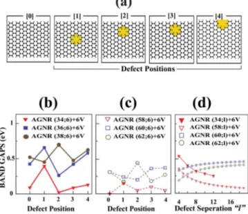
A typical hole is created by removing carbon atoms at the corners of any hexagon of an armchair ribbon and subse-quently by terminating the remaining six twofold-coordinated carbon atoms with hydrogen atoms. Figures1共a兲 and1共b兲 show that the electronic structure of AGNR共34兲 is
strongly modified by such a hole which is placed at the cen-ter of the ribbon. The hole repeats itself at each supercell which comprises six primitive cells corresponding to a repeat period of l = 6. This ribbon having a periodic hole共or defect兲 is specified as AGNR共N;l兲 and has a nonmagnetic ground state. Despite large separation of periodic defect which hin-ders their direct coupling, such a strong modification of the band gap is somehow unexpected. However, it is an indirect effect and it occurs since the itinerant共Bloch兲 states of band edges are modified by the defect. At the end, the direct band gap27at the⌫ point has widened from 0.09 to 0.40 eV due to
a defect situated at the center of the ribbon. AGNR共36兲 ex-hibits the similar behavior; namely, its band gap increases when a similar hole repeats itself at each supercell consisting of six primitive cells. In contrast, the band gap of AGNR共38兲, which is normally larger than that of AGNR共34兲, is reduced if the same hole is introduced at its center. In addition, states localized around the defect have formed flat bands near the edge of valence and conduction bands be-cause of their reduced coupling. These results are in agree-ment with previous works revealing states localized at the vacancy defect.9,19,28,29
Even more interesting is that the above effects of the hole consisting of six carbon vacancies are strongly dependent on its position relative to both edges of the nanoribbon as de-picted in Fig. 2共a兲. As shown in Fig. 2共b兲, the changes in band gap depend on N of AGNR 共in the family specified as 6m + q, with q being −2, 0, and +2兲 as well as on the position of the hole. We note that the variation in the band gap with the position of the hole relative to the edges of the ribbon shows similar trends for both AGNR共34;6兲 and AGNR共36;6兲. FIG. 1. 共Color online兲 共a兲 Energy-band structures of
AGNR共N=34; l=6兲 with and 共b兲 without a hole consisting of six carbon vacancies.共c兲 Charge-density isosurfaces of selected states. Carbon atoms共represented by black circles兲, which have coordina-tion number lower than three, are terminated by hydrogen atoms 共represented by small gray circles兲.
FIG. 2.共Color online兲 Effect of a periodic hole on the electronic structure of armchair nanoribbon. 共a兲 Positions of a hole in the ribbon are indicated by numerals. The nanoribbon without a hole is specified by “0.” Carbon atoms共black circles兲, which have coordi-nation number lower than three, are terminated by hydrogen atoms 共represented by small gray circles兲. 关共b兲 and 共c兲兴 Variations in band gaps of AGNR共N,l兲 with the position of the hole specified as 6 V. 共d兲 Variation in the band gap with repeat periodicity, l. Results for N⬍58 are obtained by first-principles calculations.
However, AGNR共38;6兲 displays different trends.
ETB calculations indicate that a similar behavior is also obtained in AGNR共N;l兲’s having relatively larger N 共i.e.,
N = 58, 60, 62兲 in Fig.2共c兲. As expected the effect of the hole on the band gap depends on the repeat periodicity. As shown in Fig. 2共d兲, the effect of defect decreases with increasing repeat periodicity l. We found that larger holes with different geometry and rotation symmetry can result in diverse elec-tronic structure and confined states. It should be noted that a repeating hole can also modify the mechanical properties. For example, the stiffness of a ribbon is reduced by the pres-ence of a hole. The force constant, =2ET/c2 共with ET
being the total energy and c being the lattice constant兲, cal-culated for AGNR共34;6兲 with a hole at its center 共 = 6.03 eV/Å2兲 is found to be smaller than that without a hole共= 7.50 eV/Å2兲.
We now show that different types of vacancies in the same armchair nanoribbon give rise to different changes in electronic and magnetic properties. A divacancy created in AGNR共22兲 can cause a dramatic change in the electronic state of the ribbon when it is repeated with the periodicity of
l = 5. Such an armchair ribbon is specified as AGNR共22;5兲.
The divacancy first relaxes and forms an eightfold ring of carbon atoms which is adjacent to six hexagons and two pentagons. In Fig. 3共a兲 we see that the nonmagnetic and semiconducting AGNR共22兲 with a band gap of EG = 0.18 eV becomes a nonmagnetic metal, since a flat band derived from the defect occurs below the top of the valance band edge and causes a metallic state. The states of this band have charge localized at the atoms surrounding the defect. Calculations performed with different repeat periods l = 3 , 4 , 5 , 10 show that the dispersion of this band decreases with increasing l. The structure including a single divacancy, which has two sublattices with equal number of carbon at-oms, NA and NB, remains bipartite even after relaxation. At the end, the net magnetic moment per unit cell is =共NA − NB兲B= 0.
The effect of a single carbon vacancy becomes even more interesting.30 A single vacancy created in AGNR共22兲 is
re-laxed and the threefold rotation symmetry is broken due to Jahn-Teller distortion. At the end, a nine-sided ring forms adjacent to a pentagon as shown in Fig. 3共b兲. All carbon atoms on this ring have threefold coordination except for the single one that remains twofold coordinated with a
sp2-dangling bond. Owing to the spin polarization of this
sp2-dangling bond and adjacent orbitals at the defect site, the system obtains an unbalanced spin. The difference of total charge density corresponding to different spin states, i.e., ⌬T=T↑−T↓ is nonzero and exhibits a distribution shown in Fig.3共b兲. Because of unbalanced spin, AGNR共22;5兲, which was nonmagnetic when perfect, gains a net magnetic mo-ment of= 1Bper unit cell. We note that this calculated net magnetic moment is in compliance with Lieb’s theorem31
since NA− NB= 1. The difference charge density, ⌬, is cal-culated for the spin-down and spin-up bands just below the Fermi level and the lower-lying spin-up band at⬃−0.5 eV. The former two bands are slight spin split and are formed from the combination of orbitals of carbon atoms sur-rounding the vacancy. The lower-lying spin-up band is de-rived mainly from the sp2-dangling bond orbital of
twofold-coordinated carbon atom. The dispersive nonmagnetic band at the edge of the valence band becomes partially emptied since its electrons are transferred to the flat spin bands below. Eventually, the semiconducting ribbon becomes metallic.
The recent work by Palacios et al.18 based on the
mean-field Hubbard model presented an extensive discussion on the effects of vacancy defects on graphene and graphene na-noribbons but only on the armchair ones. While they con-sider various vacancy defects, only the single vacancy is common between their work and the present work. In spite of the fact that they ignored the lattice distortion and as-sumed the same on-site energy for the edge, as well as for the bulk carbon atoms, our results are in overall agreement with theirs. In particular, the magnetic properties induced by the vacancy defects comply with Lieb’s theorem31 in both
FIG. 3. 共Color online兲 共a兲 Metallization of the semiconducting AGNR共22兲 by the formation of divacancies with a repeat period of l = 5.共b兲 Magnetization of the nonmagnetic AGNR共22兲 by a defect due to the single carbon atom vacancy with the same repeat peri-odicity. Isosurfaces around the vacancy corresponding to the differ-ence of the total charge density of different spin directions, ⌬T, indicate a net magnetic moment. Solid共red兲 and dashed 共red兲 lines are for spin-up and spin-down bands; solid 共black兲 lines are non-magnetic bands.
the works. As far as the effects of void on the band gap are concerned, the present discussion is unique. As we will show in Sec. III B, the situation is, however, rather different for zigzag nanoribbons.
B. Zigzag nanoribbons
Not only armchair but also zigzag nanoribbons are strongly affected by defects due to single and multiple va-cancies. When coupled with the magnetic edge states of the zigzag nanoribbons, the vacancy defect brings about addi-tional changes. The magnetic state and energy-band structure of these ribbons depend on the type and geometry of the defects. It should be noted that a sp2-dangling bond is asso-ciated with each single vacancy in Figs.4共a兲–4共e兲. The effect of a defect generated from the single vacancy with a repeat periodicity of l = 8 is examined in ZGNR共14;8兲 for three dif-ferent positions. The total energy is 0.53 eV lowered when the defect is situated at the edge rather than at the center of the ribbon.
ZGNR共14;8兲 has a net magnetic moment of = 1.94B when the defect is situated at the center of the ribbon, and hence its antiferromagnetic ground state has changed to fer-rimagnetic state through the magnetic moment of the single vacancy. Otherwise, becomes zero when the position of the defect deviates from the center. For example, in Figs. 4共b兲and4共c兲the sum of the magnetic moments of the edge states is not zero, but the net magnetic moment per unit cell becomes zero only after the spins of the defect is added. Even if the net magnetic moment = 0, ZGNR共14;8兲 does
not have an antiferromagnetic ground state due to the pres-ence of a single vacancy. The edge states, each normally having equal but opposite magnetic moments, become ferri-magnetic when a defect is introduced. The total ferri-magnetic moment of the supercell vanishes only after the magnetic moment of defect has been taken into account. Since the spin degeneracy has been broken, one can define EG↑ and EG↓ for majority and minority spin states. Not only the magnetic state but also the band gap of zigzag ribbons in Fig. 4 is affected by the symmetry and the position of the defect rela-tive to the edges.
In Figs. 4共d兲 and 4共e兲 two defects associated with two separated vacancy exhibit similar behaviors. In Fig. 4共d兲the vacancies sit in different sublattices and they have antiferro-magnetic coupling with a zero net antiferro-magnetic moment in the unit cell. On the other hand, the vacancies in Fig. 4共e兲are located in the same sublattices and they are ferromagneti-cally coupled with a net magnetic moment of 3.91B. These results obtained for the zigzag nanoribbons appear to confirm the early tight-binding studies dealing with a 2D graphene layer.18,19,28,29,32All carbon atoms surrounding the divacancy
have threefold coordination, and hence there is no
sp2-dangling bond in the defect system. It appears that the relaxed structure is bipartite, since two missing atoms asso-ciated with the divacancy are situated in different sublattices and the calculated net magnetic moment per cell is zero.
According to Lieb’s theorem the net magnetic moment per cell should be = 1B for the defect in Figs. 4共a兲–4共c兲 and= 2Bfor the case in Fig.4共e兲. None of these cases is in agreement with Lieb’s theorem. Here one can consider three features, which may be responsible from this discrep-ancy. First is the strong Jahn-Teller distortion and relaxation of carbon atoms at the close proximity of the defect. As a result some dangling sp2 bonds reconstructed to form new C-C covalent bonds. The lowering of the total energy, a driv-ing force for such reconstruction, is as high as 0.5–0.6 eV/ cell. Second is the superexchange interaction with the mag-netic edge states, which becomes effective for narrow ZGNRs. Third is the coexistence of unpaired sp2-dangling bond and orbitals due to a missing atom. Our extensive analysis showed that the zigzag nanoribbons are rather dif-ferent from armchair ones and these three features have a combined effect on the resulting net magnetic moment.
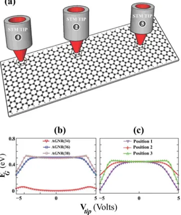
Finally, we note that introducing periodic vacancies or defects on a given ribbon appear to be difficult with the state-of-the-art technologies. Here we propose a method as described in Fig.5to achieve the formation of periodic local defects such as holes or vacancies. The sharp electrodes such as STM tips are situated at desired locations, such as one of the cases 1–3 in Fig. 5共a兲 on the graphene ribbon with a given repeat periodicity. A potential difference, Vtip, common to all electrodes 共tips兲 is applied between the tip and under-lying insulator through the ribbon. This way the electronic potential of graphene atoms just below the tip is locally low-ered or raised depending on the polarity of Vtip. Here, the effect of locally and periodically applied potential difference has been modeled by ETB, where the on-site energies of carbon atoms below the tip have been changed accordingly. Although the present model is crude, it still allows one to monitor the properties of nanoribbons. In Fig.5共b兲the varia-FIG. 4. 共Color online兲 Vacancy and divacancy formations in an
antiferromagnetic semiconductor ZGNR共14兲 with a repeat period of l = 8. Carbon atoms at both edges are terminated by hydrogen atoms represented by small gray circles. Calculated total energy, ET 共in eV/cell兲, net magnetic moment, 共in Bohr magneton B/cell兲, and band gap between spin-up共down兲 conduction and valence bands, EG↑共↓兲兲 are shown for each case. Blue and yellow isosurfaces corre-spond to the difference of spin-up and spin-down states. 关共a兲–共c兲兴 Single vacancy,关共d兲 and 共e兲兴 two separated single vacancy, and 共f兲 a divacancy.
tion in EG with Vtip is calculated for AGNR共N;20兲 with N = 34, 36, and 38 by using periodically located tips at the center of the ribbon. Because of the electron-hole symmetry in the ribbons, the band-gap variation depends on the mag-nitude of the bias voltage. In Fig. 5共c兲 the variation in the band gap of AGNR共42;20兲 with Vtip and position of the tip
are shown. In spite of the fact that the modifications of the band gaps are not the same as in Fig.2, the available param-eters, such as Vtip, l, tip geometry, and its position, make the monitoring of the properties possible.
IV. CONCLUSIONS
In conclusion, we show that the energy band gaps and magnetic states of graphene nanoribbons can be modified by the periodic defects due to single or multiple vacancies. Itin-erant共Bloch兲 states, which are perturbed by periodic vacancy defects, form dispersive bands at band edges and modify the band gap. The reconstruction of the atomic structure at the defect site is crucial for induced magnetic moments. The structural local reconstruction and spin polarization of the orbitals at the close proximity of the defect give rise to net magnetic moments, which, in turn, changes the magnetic ground state of the defect-free ribbon. The effect of the same vacancy defect on the electronic and magnetic properties de-pends on its symmetry, repeating periodicity, and position with respect to the edge of the ribbon, and it also depends on the type of the ribbon. While a nonmagnetic and semicon-ducting armchair nanoribbon can be metallized by divacancy, it becomes ferromagnetic by a single vacancy defect. The zigzag nanoribbon, which is an antiferromagnetic semicon-ductor, may become a ferrimagnetic semiconductor. How-ever, the effect of vacancy defect on the electronic and mag-netic properties of the zigzag nanoribbon varies with its symmetry, size, and position. Finally, we showed that electric field applied by an electrode perpendicular to the surface of the ribbon can induce effects similar to those due to vacancy defects.
ACKNOWLEDGMENT
Parts of the computations have been carried out by using UYBHM at Istanbul Technical University through Grant No. 2-024-2007.
1K. S. Novoselov, A. K. Geim, S. V. Morozov, D. Jiang, M. I.
Katsnelson, I. V. Grigorieva, S. V. Dubonos, and A. A. Firsov, Nature共London兲 438, 197 共2005兲.
2Y. Zhang, Y.-W. Tan, H. L. Stormer, and P. Kim, Nature
共Lon-don兲 438, 201 共2005兲.
3C. Berger, Z. Song, X. Li, X. Wu, N. Brown, C. Naud, D.
Mayou, T. Li, J. Hass, A. N. Marchenkov, E. H. Conrad, P. N. First, and W. A. de Heer, Science 312, 1191共2006兲.
4M. I. Katsnelson, K. S. Novoselov, and A. K. Geim, Nat. Phys.
2, 620共2006兲.
5A. K. Geim and K. S. Novoselov, Nature Mater. 6, 183共2007兲. 6M. Fujita, K. Wakabayashi, K. Nakada, and K. Kusakabe, J.
Phys. Soc. Jpn. 65, 1920共1996兲.
7K. Wakabayashi and M. Sigrist, Phys. Rev. Lett. 84, 3390
共2000兲.
8K. Wakabayashi, Phys. Rev. B 64, 125428共2001兲. 9K. Wakabayashi, J. Phys. Soc. Jpn. 71, 2500共2002兲.
10V. Barone, O. Hod, and G. E. Scuseria, Nano Lett. 6, 2748
共2006兲.
11Y.-W. Son, M. L. Cohen, and S. G. Louie, Nature共London兲 444,
347共2006兲.
12Y.-W. Son, M. L. Cohen, and S. G. Louie, Phys. Rev. Lett. 97,
216803共2006兲.
13M. Y. Han, B. Ozyilmaz, Y. Zhang, and P. Kim, Phys. Rev. Lett.
98, 206805共2007兲.
14K. Nordlund, J. Keinonen, and T. Mattila, Phys. Rev. Lett. 77,
699共1996兲.
15A. Hashimoto, K. Suenaga, A. Gloter, K. Urita, and S. Iijima,
Nature共London兲 430, 870 共2004兲.
16P. Esquinazi, D. Spemann, R. Höhne, A. Setzer, K.-H. Han, and
T. Butz, Phys. Rev. Lett. 91, 227201共2003兲. FIG. 5. 共Color online兲 共a兲 Monitoring of band gaps EG by
ap-plying a local bias voltage Vtipacross the ribbon.共b兲 EGversus Vtip
applied at the center of AGNR共N;6兲 for N=34, 36, and 38. 共b兲 EG versus Vtip of AGNR共34兲 for different tip positions schematically
described at the top. The tip共or electrodes兲 is situated at one of the positions 1–3. The repeat period is l = 20.
17O. V. Yazyev and L. Helm, Phys. Rev. B 75, 125408共2007兲. 18L. Brey, H. A. Fertig, and S. Das Sarma, Phys. Rev. Lett. 99,
116802共2007兲.
19M. A. H. Vozmediano, M. P. Lopez-Sancho, T. Stauber, and F.
Guinea, Phys. Rev. B 72, 155121共2005兲.
20J. J. Palacios, J. Fernández-Rossier, and L. Brey, Phys. Rev. B
77, 195428 共2008兲; for graphene nanoislands see also J.
Fernández-Rossier and J. J. Palacios, Phys. Rev. Lett. 99, 177204共2007兲.
21X. Li, L. Zhang, S. Lee, and H. Dai, Science 319, 1229共2008兲. 22X. Wang, Y. Ouyang, X. Li, H. Wang, J. Guo, and H. Dai, Phys.
Rev. Lett. 100, 206803共2008兲.
23P. E. Blochl, Phys. Rev. B 50, 17953共1994兲.
24J. P. Perdew, J. A. Chevary, S. H. Vosko, K. A. Jackson, M. R.
Pederson, D. J. Singh, and C. Fiolhais, Phys. Rev. B 46, 6671 共1992兲.
25G. Kresse and J. Hafner, Phys. Rev. B 47, 558共1993兲. 26G. Kresse and J. Furthmüller, Phys. Rev. B 54, 11169共1996兲. 27As shown by the recent work based on self-energy corrections
关L. Yang, C. H. Park, Y.-W. Son, M. L. Cohen, and S. G. Louie, Phys. Rev. Lett. 99, 186801共2007兲兴, the band gap, EG, is un-derestimated by the DFT calculations. Since we consider struc-tures which have already a band gap, its actual value does not affect our discussion in any essential manner.
28Vitor M. Pereira, F. Guinea, J. M. B. Lopes dos Santos, N. M. R.
Peres, and A. H. Castro Neto, Phys. Rev. Lett. 96, 036801 共2006兲.
29N. M. R. Peres, F. Guinea, and A. H. Castro Neto, Phys. Rev. B
73, 125411共2006兲.
30Using the definition of Schottky defect, we calculated the
forma-tion energy of relaxed vacancy of single carbon atom in AGNR共34兲 to be 7.79 eV. This value is smaller than the binding energy of a carbon atom in the graphene, which is calculated to be 9.23. However, owing to the concerted process the vacancy formation energy may be smaller than 7.79 eV.
31E. H. Lieb, Phys. Rev. Lett. 62, 1201共1989兲.
32H. Kumazaki and Dai S. Hirashi, J. Phys. Soc. Jpn. 76, 064713