www.small-journal.com
Light-Emitting Diodes with Cu-Doped Colloidal Quantum
Wells: From Ultrapure Green, Tunable Dual-Emission to
White Light
Baiquan Liu, Manoj Sharma, Junhong Yu, Sushant Shendre, Chathuranga Hettiarachchi,
Ashma Sharma, Aydan Yeltik, Lin Wang, Handong Sun, Cuong Dang,
and Hilmi Volkan Demir*
Dr. B. Liu, Dr. M. Sharma, J. Yu, S. Shendre, A. Sharma, Prof. C. Dang, Prof. H. V. Demir
Luminous! Centre of Excellence for Semiconductor Lighting and Displays School of Electrical and Electronic Engineering and School of Physical and Mathematical Sciences
Nanyang Technological University Singapore 639798, Singapore E-mail: [email protected] C. Hettiarachchi, Prof. C. Dang
Centre for OptoElectronics and Biophotonics (COEB) School of Electrical and Electronic Engineering The Photonics Institute (TPI)
Nanyang Technological University
50 Nanyang Avenue, Singapore 639798, Singapore
DOI: 10.1002/smll.201901983
properties due to the strong quantum confinement only in the vertical direc-tion. These properties include a narrow emission spectrum, suppressed inho-mogenous emission broadening, giant oscillator strength, an ultrashort radia-tive fluorescence lifetime, and extremely large linear/nonlinear absorption cross-sections.[5–8] Due to these excellent charac-teristics, CQWs have been actively studied for different optoelectronic applications including lasers, photovoltaics, and light-emitting diodes (LEDs).[9–11]
As a new type of nanocrystal LEDs, CQW-LEDs have great potential for dis-plays and lighting thanks to their merits such as outstanding color purity, low power consumption, high efficiency, and flexibility.[12–14] The first CQW-LED was emerged in 2014,[15] which was two dec-ades later than the first CQD-LED.[16] Thus, understanding why the performance of CQW-LEDs lags behind that of CQD-LEDs is not difficult. However, by virtue of the knowledge of other types of LEDs (e.g., CQD-LEDs and organic LEDs) and the increased under-standing of the photophysics of CQWs,[17–20] the development of CQW-LEDs is accelerating. To date, various architectures
Copper-doped colloidal quantum wells (Cu-CQWs) are considered a new class of optoelectronic materials. To date, the electroluminescence (EL) property of Cu-CQWs has not been revealed. Additionally, it is desirable to achieve ultrapure green, tunable dual-emission and white light to satisfy the various requirement of display and lighting applications. Herein, light-emitting diodes (LEDs) based on colloidal Cu-CQWs are demonstrated. For the 0% Cu-doped concentration, the LED exhibits Commission Internationale de L’Eclairage 1931 coordinates of (0.103, 0.797) with a narrow EL full-wavelength at half-maximum of 12 nm. For the 0.5% Cu-doped concentration, a dual-emission LED is realized. Remarkably, the dual emission can be tuned by manipulating the device engineering. Fur-thermore, at a high doping concentration of 2.4%, a white LED based on CQWs is developed. With the management of doping concentrations, the color tuning (green, dual-emission to white) is shown. The findings not only show that LEDs with CQWs can exhibit polychromatic emission but also unlock a new direction to develop LEDs by exploiting 2D impurity-doped CQWs that can be further extended to the application of other impurities (e.g., Mn, Ag).
Quantum Wells
Dr. A. Yeltik, Prof. H. V. Demir
Department of Electrical and Electronics Engineering Department of Physics
UNAM-Institute of Materials Science and Nanotechnology Bilkent University
Ankara 06800, Turkey Dr. L. Wang, Prof. H. Sun
Division of Physics and Applied Physics School of Physical and Mathematical Sciences Nanyang Technological University
Singapore 637371, Singapore
The ORCID identification number(s) for the author(s) of this article can be found under https://doi.org/10.1002/smll.201901983.
Colloidal quantum wells (CQWs), also referred to as semicon-ductor nanoplatelets (NPLs) or atomically flat nanocrystals, have been revealed as a new family of 2D nanocrystals in the past few years.[1–4] Unlike colloidal quantum dots (CQDs), CQWs exhibit many unique thickness-dependent optical
(e.g., core-only, core/shell, and core/crown) based CQWs have been used for LEDs. For example, Fan et al. fabricated an LED with CdSe1−xSx alloyed core-only CQWs, achieving
a maximum luminance of ≈90 cd m−2, which is currently the best value for inverted green CQW-LEDs.[21] Furthermore, we previously reported a red LED with CdSe/CdSe0.8Te0.2 core/ crown type II CQWs, obtaining a maximum external quantum efficiency (EQE) of 3.57%.[22] More recently, Giovanella et al. reported a deep-red LED by adopting CdSe/CdZnS core/shell CQWs, yielding an EQE of 8.39% and a maximum luminance of ≈100 cd m−2.[23] Therefore, CQW-LEDs have great potential to show high performance. However, despite the tendency of CQW-LEDs to furnish saturated red colors, the reported green color is not sufficiently pure. In addition, the previous CQW-LEDs only exhibited monochromatic electroluminescence (EL), with no chance of dual emission. Furthermore, white emission based on CQWs has not been documented. Hence, a large gap between CQW-LEDs and other types of LEDs still exists.
Since the human eye is more sensitive to green than to blue/red colors, meeting the demand of the International Tel-ecommunication Union Recommendation BT 2020 (Rec. 2020) standard for new-generation ultrahigh definition TVs is chal-lenging for green LEDs.[24] To loosen this bottleneck, many efforts have been made to enlarge the color gamut which is defined by the corresponding three color primaries (e.g., the Commission Internationale de L’Eclairage (CIE) 1931 color coordinates of (0.170, 0.797) for the Rec. 2020 standard green emitter).[24] For instance, Kumar et al. demonstrated a green LED with 2D formamidinium lead bromide hybrid perovskites, achieving a color gamut covering 96.8% of the Rec. 2020 standard in the CIE 1931 color space, which is the “greenest” LED reported thus far.[25] Using supercrystal inorganic perov-skites, Tong et al. also reported an LED exhibiting a color close to the Rec. 2020 pure green.[26] On the other hand, dual-emission colloidal semiconductor nanocrystals are of interest for applica-tions in multimodal imaging, sensing, lighting, and integrated photonics.[27–29] However, the best EQE of single-nanocrystal LEDs with dual emission cannot exceed 0.100%.[30] In addition, no report that the dual emission of single-nanocrystal LEDs can be tuned by manipulating the device engineering exists. Fur-thermore, although white emission is desirable for lighting and high-quality displays, the study of white LEDs (WLEDs) based on CQWs remains unexplored. Therefore, a question arises: is it possible for CQW-LEDs to produce ultrapure green, tunable dual-emission and white EL?
Impurity doping is a widespread method to afford semi-conductor nanocrystals possessing new optical, electronic, and magnetic characteristics.[31] Over the last decade, many endeavors have been undertaken in the development of Cu-doped 0D and 1D nanocrystals.[32–34] Recently, we have reported Cu-doped 2D CQWs and showed that they are promising for solar light harvesting technologies.[35] However, the effect of Cu-doped CQWs in LEDs has not yet been elucidated. In fact, no LED based on impurity-doped CQWs has been reported thus far.
In this paper, for the first time, LEDs based on Cu-doped CQWs have been developed. Specifically, by controlling the Cu concentration in CdSe CQWs, the Cu-doping effect in LEDs has been revealed. For the 0% Cu-doped concentration, the
LED exhibits the CIE 1931 coordinates of (0.103, 0.797). Sig-nificantly, the full-wavelength at half-maximum (FWHM) of the EL emission is as narrow as 12 nm. For a 0.5% Cu-doped concentration, the LED possesses dual emission with an EQE of 0.146%. To the best of our knowledge, i) this LED is the first CQW-LED possessing dual emission, ii) the efficiency is the best for single-nanocrystal LEDs with dual emission, iii) the approach is a new one to vastly enhance the performance of CQW-LEDs via impurity doping (i.e., realizing nine times higher EQE than the 0% concentration-based device). Impres-sively, this dual emission can be tuned by manipulating the device engineering, which is an unexplored emission mecha-nism for single-nanocrystal LEDs. Moreover, at a high Cu-doped concentration of 2.4%, a new WLED based on CQWs has been demonstrated.
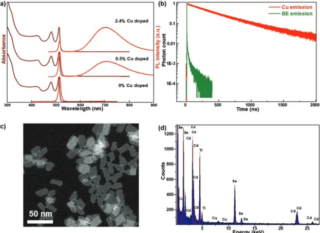
Cu-doped CdSe CQWs were synthesized by a high-tem-perature nucleation doping method recently reported by our group.[35] Further details of the syntheses can be found in the Supporting Information. The optical properties of these undoped and Cu-doped CQWs were characterized via UV-vis absorption and photoluminescence (PL) spectros-copy. Figure 1a shows the steady-state UV-vis absorption and PL emission spectra of 0%, 0.5%, and 2.4% Cu-doped CdSe CQWs. The atomic ratio of Cu dopant ions with respect to total cations (Cu+Cd) was measured by inductively coupled plasma mass spectrometry (ICP-MS). The sharp excitonic features at ≈480 and ≈512 nm observed in the absorption spectra of the CQWs are associated with the light hole and electron-heavy hole transitions, respectively. With successful Cu-doping in 4 ML CdSe CQWs, a broad and Stokes-shifted emission peak (≈700 nm) appears along with the usual excitonic band-edge emission peak (≈515 nm).[35] With an increase in the Cu doping value, the contribution of the dopant emission increases with respect to the total integrated emission (excitonic +Cu dopant emission). For 0.5% Cu-doped CdSe CQWs, decay traces at the excitonic (515 nm) and dopant (700 nm) emissions were obtained using time-resolved fluorescence spectroscopy. Clearly, the dopant emission shows a long excited state lifetime compared to the order-of-magnitude-faster excitonic lifetime (Figure 1b, Tables S1 and S2, Supporting Information). Further-more, the absence of a fast lifetime decay channel (≈10–20 ns) for the dopant emission clearly indicates efficient dopant emis-sion in these CQWs (Table S2, Supporting Information). The origin of this highly efficient and Stokes-shifted emission has been discussed in detail in our previous work.[35] The Cu-doped CdSe CQWs exhibit a roughly rectangular shape, as seen from the high-angle annular dark-field scanning transmission elec-tron microscopy (HAADF-STEM) image shown in Figure 1c. The average dimensions measured from the STEM image are 32.0 × 13.5 nm2. To estimate the Cu doping concentration, by using STEM-based energy-dispersive X-ray spectroscopy (EDX), we estimated the Cu atomic percentage to be 1.1% with respect to cadmium levels for a lightly doped sample, which shows a higher value as compared with ICP-MS results discussed above (Figure 1d). Therefore, in the whole study we show Cu doping levels by ICP:MS measurements unless otherwise stated.
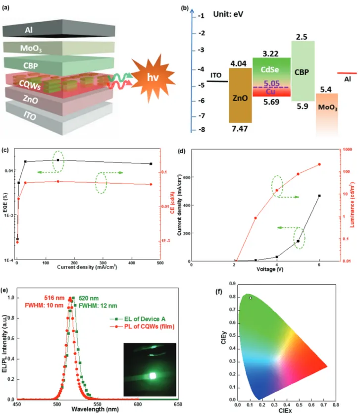
The device architecture of the CQW-LEDs is indium tin oxide (ITO)/zinc oxide (ZnO)/CQWs/4,4-N,N-dicarbazolebiphenyl (CBP)/MoO3/Al, where ITO serves as the cathode, ZnO as the
electron transport layer, the CQWs as the emitting layer (EML), CBP as the hole transport layer (HTL), MoO3 as the hole injec-tion layer, and Al as the anode, as shown in Figure 2a. Given the high electron mobility of ZnO (1.8 × 10⁻³ cm2 V−1 s−1)[18] and high hole mobility of CBP (1.0 × 10⁻³ cm2 V−1 s−1),[22] together with the fact that the barrier between the charge trans-port layers and CQWs is not high (Figure 2b), both electrons and holes can efficiently arrive at the EML. Therefore, with this configuration, charges can be effectively transported to the CQWs to generate excitons, which is beneficial for exploring the effect of Cu-doped CQWs in LEDs.
To examine the electrical characteristics, CdSe CQWs with a 0% Cu-doped concentration were first used as the emitter for LEDs (Device A). A cross-sectional scanning electron micro-scope image of Device A is depicted in Figure S1 (Supporting Information). As shown in Figure 2c and Table 1, the maxi mum EQE and current efficiency (CE) of Device A are 0.016% and 0.055 cd A−1, respectively. In addition, the maximum power efficiency (PE) is 0.040 lm W−1 (Figure S2a, Supporting Infor-mation). Notably, these efficiencies are the highest reported for inverted green CQW-LEDs. Additionally, the driving voltage is very low. For example, the turn-on voltage (the voltage when the luminance can be detected, ≥0.01 cd m−2) is approximately 2.1 V, which is among the lowest values reported for nanocrystal-based LEDs. This voltage is lower than the bandgap of CdSe CQWs (2.47 eV), which can be called as sub-bandgap voltage.[21]
Such sub-bandgap voltage has also been observed by other groups, which can be attributed to the efficient charge injec-tion at low bias (i.e., the use of effective ZnO and CBP charge transport layers ensure the charge injection in our LEDs).[36] The voltage is about 3.1 V when the luminance is 1 cd m−2. Remarkably, the maximum luminance is 210 cd m−2 (Table S3, Supporting Information), which is >2 times higher than that of the best inverted green CQW-LED.[21] As shown in Figure 2e,f, Device A exhibits a green EL emission with the CIE 1931 coor-dinates of (0.103, 0.797). As a result, the color gamut covers 104% of the Rec. 2020 standard in the CIE 1931 color space, demonstrating the purest green emission ever reported.[25,26] In terms of the National Television System Committee standard, the color gamut is as high as 123% in the CIE 1931 color space. Significantly, the FWHM of the EL emission is only 12 nm. Such extremely narrow emission may be attributed to the fact that CdSe CQWs possesses strong quantum confinement in 1D due to their fixed vertical thickness at atomic levels.[1] By com-parison with previous reports of the narrowest EL FWHMs for different types of LEDs (e.g., 16 nm for CsPbBr3 green perov-skite LEDs,[37] 14 nm for PEA
2PbBr4 LEDs,[38] and 15.3 nm for 3D perovskite thin film LEDs[39]), CdSe-based CQW-LEDs have been demonstrated here to show superior color purity.
By doping 0.5% Cu into CdSe CQWs, an LED based on this emitter was developed (Device B), where the architecture of Device B is similar to that of Device A except for the EML.
Figure 1. a) Room-temperature absorption and PL emission spectra of CQWs with different Cu concentrations in hexane solution. b) Time-resolved fluorescence decay traces of 0.5% Cu-doped CQWs at the band-edge (BE) and dopant emissions. c) HAADF-STEM image of the Cu-doped CdSe CQWs with a 0.5% Cu concentration. d) STEM-EDX spectra of 0.5% Cu-doped CQWs.
As shown in Figure 3a, the maximum EQE of Device B is 0.146%, which is nine times greater than that of Device A and is the highest reported value for single-nanocrystal LEDs
with dual emission.[30] Previously, Chen et al. achieved a two-fold increase in the EQE of CQW-LEDs by exchanging the long ligands of CQWs with short ones,[15] while Giovanella et al.
Figure 2. a) Schematic architecture of CQW-LEDs. b) The proposed energy levels of CQW-LEDs. The unit of energy is eV. The values are taken from the literature.[18,22,40–42] c) EQE and CE of Device A. d) Current density and luminance of Device A. e) The EL spectrum of Device A and the PL spectrum
of CdSe CQWs with a 0% Cu-doped concentration film. Compared with the PL spectrum of the film, with an emission of 516 nm and an FWHM of 10 nm, the EL spectrum of Device A is slightly redshifted (520 nm), and the EL FWHM is relatively widened (12 nm). Inset: a photograph of Device A under bias. f) The CIE 1931 coordinates of Device A in the color space.
obtained a 1.5-fold increase in EQE by exposing CQW-LEDs to air.[23] Here, we have accomplished a ninefold increase in EQE by doping impurities into CQWs, unlocking a new strategy to vastly enhance the efficiency of CQW-LEDs. Since the error of EQE can be analyzed by the reproducibility,[18] we have meas-ured the reproducibility of Devices A and B. As shown by the histograms of maximum EQE taken from 18 devices, the repro-ducibility of devices is good (Figure S3, Supporting Informa-tion). Additionally, the maximum CE, PE, and luminance of Device B are 0.282 cd A−1 (Figure 3a), 0.179 lm W−1 (Figure S2b, Supporting Information), and 1153 cd m−2 (Figure 3b), respec-tively, which are much higher than those of Device A. The maximum current density of Device B is 1536 mA cm−2 (9.8 V), which is higher than that of Device A (466 mA cm−2, 6.0 V). Hence, the doped LEDs exhibit a better stability than undoped ones since high voltage usually causes high working tempera-ture (Joule heating).[43] Furthermore, because the stability can be judged from the half-lifetime of devices,[18] we have meas-ured the lifetime at an initial luminance of 210 cd m−2, where the voltages are 6.0 and ≈6.3 V for Devices A and B, respectively. As expected, the lifetime of Device B is 120 s, which is much better than that of Device A (20 s). However, the high tempera-ture is detrimental to the efficiency of LEDs, leading to an effi-ciency droop. In addition, the charge balance may be weaker at high voltage, which is another factor for the efficiency droop.[44] Given that using the terminology of turn-on is dependent on sensitivity or dynamic range of instruments, the utilization of operating voltage requirement to achieve a specific current den-sity is also a good practice.[45] For example, the current density of 1 mA cm−2 is achieved at 2.1 and ≈2.9 V for Devices A and B, respectively. This fact may suggest that the current density of devices is lowered due to the effect of Cu dopant. As shown in Figure 3c, Device B can exhibit dual EL emissions at various voltages, where the peaks at ≈516 and ≈692 nm originate from the host CdSe and Cu+ ions, respectively.
The fact that the efficiency of CQW-LEDs can be vastly enhanced via impurity doping is an unprecedented phenom-enon. To understand this phenomenon, the emission mecha-nism of Device B was revealed. The PL quantum yield (PLQY) of the 0.9% Cu-doped CQWs used for LEDs (48.5%) is higher than that of the 0% Cu-doped CQWs utilized for LEDs (10%), which can be attributed to the fact that the Cu doping results in an additional dominant radiative decay channel that is induced by mid-gap Cu(I) states.[35] Importantly, the PLQYs of Cu-doped CdSe CQWs that are obtained after one cleaning
of the synthesized samples are quite high (≈80%). However, the doped CQWs used for our EL devices are typically cleaned three times with ethanol to remove excess ligand, which in turn helps to form better films in devices. The doped CQWs main-tain fairly high PLQYs (≈40–50%) even after excessive cleaning. Therefore, since the EQE is in direct proportion to the PLQY of the emitter,[22] the efficiency of Device B is greatly enhanced. In addition, as shown in Figure 3d, the Cu energy level (5.05 eV) is higher than the valance band maximum (VBM) of CdSe (5.69 eV), indicating that the holes transported from CBP are more easily trapped by Cu under a low electrical field.[44] Then, the holes meet the elec-trons transported from ZnO in the conduction band minimum (CBM) to generate excitons that recombine to produce the Cu+ emission. With increasing electrical field, holes trapped by Cu can be saturated, leading to relatively more holes transported from CBP being injected into the VBM of CdSe after satura-tion at the dopant site. These analyses can be confirmed by the EL spectra of Device B, as the Cu+ emission is lowered with increasing voltage (Figure 3c). To further verify the trapping effect of Cu, the current densities of Devices A and B were compared (Figure S4, Supporting Information). As expected, the current density of Device B is lower than that of Device A, which indicates the trapping effect.[44] From the current den-sity–voltage characteristics as shown in Figure S4 (Supporting Information), we can estimate that the slope of Device B is nearly 0.5 times that of Device A. This implies that the ideality factor for the Device B is nearly twice that of Device A which suggests that Cu-doping acts as an impurity defect site.[46]
Therefore, two decay channels for exciton recombination exist in Device B (i.e., the excitons are recombined from the electrons of the CdSe CBM and the holes of the Cu level to produce Cu+ emission or the excitons are recombined from the electrons of the CdSe CBM and the holes of the CdSe VBM to produce CdSe emission), which guarantee green/red dual emission, as shown in Figure 3c. Although holes are favored to be harvested by Cu+ at low electrical fields, exciton recom-bination in CdSe and Cu+ occurs simultaneously, which can be confirmed by the EL spectrum at the turn-on voltage. As shown in Figure S5 (Supporting Information), both CdSe and Cu+ emissions can be distinguished at 2.1 V. In the case of solution-processed LEDs, the surface roughness of the active layer plays an important role in the device performance. By using the atomic force microscopy, the root mean square roughness for the undoped CQW film is 4.02 nm (Figure S6, Supporting Information), which is higher than that of Cu-doped film (3.89 nm). These values are consistent with pre-vious papers (e.g., 3.65 nm for Fan’s CQW films[21]). Hence, the improved morphology is another reason for the enhanced EQE of Device B,[47] apart from the better PLQY of emitters and the simultaneous exciton recombination at the CdSe band edge and Cu dopant.
Previously, the dual emission of LEDs can be tuned via material design (i.e., adjusting the material compositions of emitters), which are easily understandable.[5,15,21] For the case
Table 1. Summary of LED performances.
Device EMLa) EQE
maxb) [%] CEmaxc) [cd A−1] PEmax d) [lm W−1] Von e) [V] Lmaxf) [cd m−2] A 0% Cu-doped CQWs 0.016 0.055 0.040 2.1 210 B 0.5% Cu-doped CQWs 0.146 0.282 0.179 2.4 1153 E ZnCdS/ZnS CQDs: 2.4% Cu-doped CQWs 0.029 0.025 0.020 2.3 148
a)The EML used in LEDs; b)Maximum EQE; c)Maximum CE; d)Maximum PE; e)Turn-on voltage; f)Maximum
of our Cu-doped NPLs, simultaneous appearance of excitonic and dopant emission (i.e., dual emission) in the EL spectrum suggests further investigations are needed for understanding their origin. To this end, an LED using 60 nm 1-bis[4-[N,N-di(4-tolyl)amino]phenyl]-cyclohexane (TAPC) as the HTL was developed (Device C), where the architecture of Device C is
similar to that of Device B except for the HTL. As shown in Figure 3e, the EL emission peak of CdSe (excitonic emission) is lower than that of Cu+ in Device C, which is unlike Device B since the EL peak of CdSe is higher than that of Cu+ even at the turn-on voltage. In particular, the CdSe excitonic emission is almost prohibited at the turn-on voltage in Device C (Figure S7,
Figure 3. a) EQE and CE of Device B. b) Current density and luminance of Device B. c) EL spectra of Device B at various voltages. d) Schematic of the emission mechanism of Device B. The unit of energy is eV. e) EL spectra of Device C at various voltages. f) Schematic of the emission mechanism of Device C. The unit of energy is eV.
Supporting Information). Such surprising phenomena suggest that the dual emission from the Cu-doped CQWs can be tuned by deliberately selecting the charge transport layers. Therefore, device engineering is a novel strategy to tune the dual emission of single-nanocrystal LEDs. Since many organic or inorganic charge transport materials exist, using our strategy to tune the dual emissions is very feasible. Thus, apart from the use of an “electrical field” and “material design,” “device engineering” may show unique merits for tunable emissions.
The surprising phenomena can be explained as follows. As shown in Figure 3f, since the highest occupied molecular orbital (HOMO) of TAPC (5.4 eV) is located between the Cu level (5.05 eV) and the VBM of CdSe (5.69 eV),[48] holes trans-ported from TAPC are readily injected into Cu due to the bar-rier-free characteristic. However, injecting holes into CdSe is difficult because of the hole barrier between TAPC and CdSe (0.29 eV). Hence, excitons are almost only generated and recombined to produce Cu+ emission at a low electrical field. Moreover, even at a strong electrical field, the CdSe emission is not very prominent compared with the Cu+ emission due to the existing hole barrier. These facts imply that the dual emission can be tuned via device engineering, providing deep insight into the emission mechanism of single-nanocrystal LEDs.
To reveal the effect of a high impurity doping concentration in LEDs, CdSe CQWs with a 2.4% Cu doping concentration were used as the emitter to fabricate an LED (Device D), where the architecture of Device D is the same as that of Device A except for the EML. As shown in Figure S8 (Supporting Infor-mation), dual emission can be produced at different voltages. Moreover, compared with the PL spectra, the EL emission is redshifted, with peaks at ≈520 and ≈716 nm originating from CdSe and high doping Cu+ ions, respectively. In particular, the redshift of the Cu EL peak in Device D is more obvious than that in Device B, as higher Cu doping concentrations can lower the CBM of CdSe due to orbital hybridization.[49,50] In addition, a stronger Cu+ emission can be observed in Device D. How-ever, despite the higher doping concentration, the emission mechanism of Device D is similar to that of Device B (i.e., Cu functions as a hole trapping center). This fact is further con-firmed by the EL spectra of Device D, in which the Cu emission decreases with increasing voltage.
Furthermore, with the encouragement of dual emission from Cu-doped CQWs, we expected that white emission could be generated by combining the 2.4% Cu-doped CdSe CQWs with a blue emitter. Therefore, by selecting ZnCdS/ZnS core/shell CQDs as the blue emitter, an LED was developed (Device E), where the architecture of Device E is the same as that of Device A except for the EML with the mixing ratio of CQD:CQWs = 5:1 (in wt%). ZnCdS/ZnS core/shell CQDs were synthesized by following an earlier reported procedure,[51] and the absorp-tion and PL spectra of ZnCdS/ZnS are depicted in Figure S9 (Supporting Information), with a PL peak at 475 nm. As shown in Figure 4a–c, the maximum EQE, CE, PE, and luminance of Device E are 0.029%, 0.025 cd A−1, 0.020 lm W−1, and 148 cd m−2, respectively. In addition, a turn-on voltage of 2.3 V is obtained, which is among the lowest nanocrystal WLEDs. Remarkably, Device E exhibits white emission, where the blue emission with a peak at 480 nm originates from ZnCdS/ZnS CQDs, and the green/red emissions result from the Cu-doped
CQWs (Figure 4d). To the best of our knowledge, this is the first WLED based on CQWs. Impressively, a maxi mum color rendering index (CRI) of 62 is obtained, which is the highest reported for WLEDs using two Cd-based nanocrys-tals. According to Gnade et al.’s report,[52] a CRI > 60 is accept-able for applications. Additionally, ≥3 nanocrystals are usually required for high CRIs, which inevitably increases the com-plexity of WLEDs.[53] Although WLEDs using two nanocrystals are more simplified and desirable for low-cost commerciali-zation, their CRI is generally low (e.g., CRI = 14.7 for Bae’s WLED with two CQDs[54]). Therefore, our results provide a novel avenue toward simplified but high-CRI WLEDs.
To further understand the WLED based on CQWs, the exciton decays in Device E were analyzed. Device E pos-sesses a hybrid architecture since ZnO and CBP are inorganic and organic charge transport layers, respectively.[36] In addi-tion, since the amount of ZnCdS/ZnS CQDs is much higher than that of CQWs, the charge injection is greatly affected by ZnCdS/ZnS. Moreover, because the electron barrier between the CBMs of ZnO and ZnCdS/ZnS (3.6 eV) is lower than the hole barrier between the HOMO of CBP and the VBM of ZnCdS/ZnS (6.4 eV),[55] the electron injection from ZnO to ZnCdS/ZnS is more effective than the hole injection from CBP to ZnCdS/ZnS. As a result, charge imbalance occurs by further considering that the electron mobility of ZnO is higher than the hole mobility of CBP. This leads to nonradiative Auger recombination, which is detrimental to the efficiency.[36] For the Cu-doped CdSe CQWs, the CdSe and Cu levels are lower than the HOMO of CBP and the VBM of ZnCdS/ZnS, which is favorable for hole injection. With enhanced electric field, popu-lated holes in CQWs can hop into ZnCdS/ZnS, mitigating the charge imbalance.[53] Hence, the CQWs can contribute to sup-pressing the Auger decay and enhancing the radiative exciton recombination.
Since two emitters have been mixed in Device E, excitons can be transferred from large-bandgap emitters to small-bandgap emitters via the Förster procedure.[53] Thus, the amount of ZnCdS/ZnS CQDs is fivefold higher than that of CQWs to guar-antee white emission because the high-energy excitons from ZnCdS/ZnS are readily transferred to the CQWs. To verify this Förster resonant energy transfer (FRET) process, the absorp-tion spectrum of the CQWs and the PL spectrum of the ZnCdS/ ZnS CQDs were compared.[56] As shown in Figure S10 (Sup-porting Information), a large overlap exists between these two spectra, indicating the efficient FRET in Device E.[53] However, our ZnCdS/ZnS is not sufficiently efficient, which limits the efficiency of Device E. To provide evidence for this, a blue LED based on ZnCdS/ZnS CQDs was fabricated (Device F), where the architecture of Device F is the same as that of Device E except for the EML of ZnCdS/ZnS. As shown in Figure S11 (Sup-porting Information), the maximum EQE of Device F is only 0.209%. Therefore, to further enhance the efficiency of WLEDs based on CQWs, a facile method is the introduction of highly efficient blue emitters. In addition, by tuning the ratio of CQWs and ZnCdS/ZnS CQDs, other white emissions can be obtained, indicating a flexible scheme to achieve WLEDs. For example, a cooler white emission with the CIE coordinates of (0.22, 0.25) is produced in Device G (Figure S12, Supporting Information), where the architecture of Device G is the same as that of Device E
except for the EML with the ratio of CQDs:CQWs = 10:1. The findings imply that the CQWs can directly operate with the CQDs as the EML and that white emissions can be facilely fur-nished by adjusting the ratio of CQWs and CQDs, thus bridging the relation between 2D CQWs and 0D CQDs. Furthermore, by using different dopant combinations in CQWs (e.g., Mn-, Ag-doped CdSe CQWs), the emission spectrum of the dopant is expected to be tuned into a more visible region, which can enable achievement of further high performance and CRI. Finally, it is worth mentioning that the operation lifetime of CQW-LEDs has never been reported, which may be attributed to the instability of CQW-LEDs. The lifetime of our devices made from core-only doped-CQWs is smaller (e.g., 270 s at 100 cd m−2). This is com-parable to similar undoped CQWs and is only a little longer than some perovskite LEDs (e.g., 80 s).[57] However, with CQW het-erostructures (e.g., core/shell, core/crown) synthesized by col-loidal atomic layer deposition or hot injection methods, LEDs from these doped-CQWs are expected to show high operational lifetime, which are under investigation.
To conclude, LEDs of Cu-doped CQWs have been success-fully developed. For the 0% Cu-doped concentration, the color gamut of the LED can cover 104% of the Rec. 2020 standard in the CIE 1931 color space. Significantly, the EL FWHM is as narrow as 12 nm. With the 0.5% Cu-doped concentration, a CQW-LED with dual emission has been reported. Impressively, the dual emission can be tuned via device engineering, which is an unreported mechanism for single-nanocrystal LEDs. More-over, with the 2.4% Cu-doped concentration, the WLED based on CQWs has been demonstrated. Such results undrape new advantages of CQW-LEDs, begin the step that LEDs based on CQWs can possess polychromatic emission apart from previous discovered monochromatic emission, and open a new avenue to
realize LEDs by employing 2D impurity-doped CQWs that can be further extended to the use of other impurities (e.g., Mn, Ag).
Supporting Information
Supporting Information is available from the Wiley Online Library or from the author.
Acknowledgements
B.L. and M.S. contributed equally to this work. The authors declare no competing financial interest. This research is supported by the National Research Foundation, Prime Minister’s Office, Singapore under its Investigatorship program (NRF-NRFI2016-08) and the Singapore Agency for Science, Technology and Research (A*STAR) SERC Pharos Program under grant no. 152 73 00025. H.V.D. gratefully acknowledges TUBA. The authors thank ACS ChemWorx Authoring Services (https:// es.acschemworx.acs.org/en/) for providing linguistic assistance during the preparation of this manuscript.
Conflict of Interest
The authors declare no conflict of interest.
Keywords
colloidal quantum wells, dual emission, impurity doping, light-emitting diodes, nanoplatelets
Received: April 20, 2019 Revised: June 28, 2019 Published online: August 5, 2019 Figure 4. The EL characteristics of Device E. a) EQE and CE, b) power efficiency (PE), c) current density and luminance, and d) EL spectrum. Inset: photograph of Device E under bias.
[1] S. Ithurria, M. D. Tessier, B. Mahler, R. P. S. M. Lobo, B. Dubertret, A. L. Efros, Nat. Mater. 2011, 10, 936.
[2] J. Q. Grim, S. Christodoulou, F. Di Stasio, R. Krahne, R. Cingolani, L. Manna, I. Moreels, Nat. Nanotechnol. 2014, 9, 891.
[3] C. E. Rowland, I. Fedin, H. Zhang, S. K. Gray, A. O. Govorov, D. V. Talapin, R. D. Schaller, Nat. Mater. 2015, 14, 484.
[4] A. Riedinger, F. D. Ott, A. Mule, S. Mazzotti, P. N. Knusel, S. J. P. Kress, F. Prins, S. C. Erwin, D. J. Norris, Nat. Mater. 2017,
16, 743.
[5] D. V. Talapin, J.-S. Lee, M. V. Kovalenko, E. V. Shevchenko, Chem.
Rev. 2010, 110, 389.
[6] M. D. Tessier, C. Javaux, I. Maksimovic, V. Loriette, B. Dubertret,
ACS Nano 2012, 6, 6751.
[7] B. Mahler, B. Nadal, C. Bouet, G. Patriarche, B. Dubertret, J. Am.
Chem. Soc. 2012, 134, 18591.
[8] M. D. Tessier, P. Spinicelli, D. Dupont, G. Patriarche, S. Ithurria, B. Dubertret, Nano Lett. 2014, 14, 207.
[9] L. T. Kunneman, J. M. Schins, S. Pedetti, H. Heuclin, F. C. Grozema, A. J. Houtepen, B. Dubertret, L. D. A. Siebbeles, Nano Lett. 2014,
14, 7039.
[10] C. She, I. Fedin, D. S. Dolzhnikov, P. D. Dahlberg, G. S. Engel, R. D. Schaller, D. V. Talapin, ACS Nano 2015, 9, 9475.
[11] F. T. Rabouw, J. C. Bok, P. Spinicelli, B. Mahler, M. Nasilowski, S. Pedetti, B. Dubertret, D. Vanmaekelbergh, Nano Lett. 2016, 16, 2047.
[12] L. Jing, S. V. Kershaw, Y. Li, X. Huang, Y. Li, A. L. Rogach, M. Gao,
Chem. Rev. 2016, 116. 10623.
[13] Y. Ling, Z. Yuan, Y. Tian, X. Wang, J. C. Wang, Y. Xin, K. Hanson, B. Ma, H. Gao, Adv. Mater. 2016, 28, 305.
[14] C. Qin, T. Matsushima, A. S. Sandanayaka, Y. Tsuchiya, C. Adachi,
J. Phys. Chem. Lett. 2017, 8, 5415.
[15] Z. Chen, B. Nadal, B. Mahler, H. Aubin, B. Dubertret, Adv. Funct.
Mater. 2014, 24, 295.
[16] V. L. Colvin, M. C. Schlamp, A. P. Alivisatos, Nature 1994, 370, 354. [17] Y. X. Yang, Y. Zheng, W. R. Cao, A. Titov, J. Hyvonen, J. R. Manders,
J. G. Xue, P. H. Holloway, L. Qian, Nat. Photonics 2015, 9, 259. [18] X. L. Dai, Z. X. Zhang, Y. Z. Jin, Y. Niu, H. J. Cao, X. Y. Liang,
L. W. Chen, J. P. Wang, X. G. Peng, Nature 2014, 515, 96.
[19] B. Liu, L. Wang, D. Y. Gao, J. H. Zou, H. L. Ning, J. B. Peng, Y. Cao,
Light: Sci. Appl. 2016, 5, e16137.
[20] Z. Shi, S. Li, Y. Li, H. Ji, X. Li, D. Wu, T. Xu, Y. Chen, Y. Tian, Y. Zhang, C. Shan, G. Du, ACS Nano 2018, 12, 1462.
[21] F. Fan, P. Kanjanaboos, M. Saravanapavanantham, E. Beauregard, G. Ingram, E. Yassitepe, M. M. Adachi, O. Voznyy, A. K. Johnston, G. Walters, G. Kim, Z.-H. Lu, E. H. Sargent, Nano Lett. 2015, 15, 4611.
[22] B. Liu, S. Delikanli, Y. Gao, D. Dede, K. Gungor, H. V. Demir, Nano
Energy 2018, 47, 115.
[23] U. Giovanella, M. Pasini, M. Lorenzon, F. Galeotti, C. Lucchi, F. Meinardi, S. Luzzati, B. Dubertret, S. Brovelli, Nano Lett. 2018,
18, 3441.
[24] R. Zhu, Z. Luo, H. Chen, Y. Dong, S.-T. Wu, Opt. Express 2015, 23, 23680.
[25] S. Kumar, J. Jagielski, N. Kallikounis, Y.-H. Kim, C. Wolf, F. Jenny, T. Tian, C. J. Hofer, Y.-C. Chiu, W. J. Stark, T.-W. Lee, C.-J. Shih, Nano
Lett. 2017, 17, 5277.
[26] Y. Tong, E.-P. Yao, A. Manzi, E. Bladt, K. Wang, M. Doblinger, S. Bals, P. Muller-Buschbaum, A. S. Urban, L. Polavarapu, Adv.
Mater. 2018, 30, 1801117.
[27] M. Lorenzon, V. Pinchetti, F. Bruni, W. K. Bae, F. Meinardi, V. I. Klimov, S. Brovelli, Nano Lett. 2017, 17, 1071.
[28] V. Pinchetti, F. Meinardi, A. Camellini, G. Sirigu, S. Christodoulou, W. K. Bae, F. D. De Donato, L. Manna, M. Zavelani-Rossi, I. Moreels, V. I. Klimov, S. Brovelli, ACS Nano 2016, 10, 6877.
[29] Q. Lin, N. S. Makarrov, W.-K. Koh, K. A. Velizhanin, C. M. Cirloganu, H. Luo, V. I. Klimov, J. M. Pietryga, ACS Nano 2015, 9, 539.
[30] S. Brovelli, W. K. Bae, C. Galland, U. Giovanella, F. Meinardi, V. I. Klimov, Nano Lett. 2014, 14, 486.
[31] R. Xie, X. Peng, J. Am. Chem. Soc. 2009, 131, 10645.
[32] V. A. Vlaskin, N. Janssen, J. V. Rijssel, R. Beaulac, D. R. Gamelin,
Nano Lett. 2010, 10, 3670.
[33] A. H. Khan, A. Dalui, S. Mukherjee, C. U. Segre, D. D. Sarma, S. Acharya, Angew. Chem., Int. Ed. 2015, 54, 2643.
[34] K. E. Knowles, K. H. Hartstein, T. B. Kilburn, A. Marchioro, H. D. Nelson, P. J. Whitham, D. R. Gamelin, Chem. Rev. 2016, 116, 10820.
[35] M. Sharma, K. Gungor, A. Yeltik, M. Olutas, B. Guzelturk, Y. Kelestemur, T. Erdem, S. Delikanli, J. R. McBride, H. V. Demir,
Adv. Mater. 2017, 29, 1700821.
[36] B. S. Mashford, M. Stevenson, Z. Popovic, C. Hamilton, Z. Zhou, C. Breen, J. Steckel, V. Bulovic, M. Bawendi, S. Coe-Sullivan, P. T. Kazlas, Nat. Photonics 2013, 7, 407.
[37] B. Liu, L. Wang, H. Gu, H. Sun, H. V. Demir, Adv. Opt. Mater. 2018,
6, 1800220.
[38] D. Liang, Y. Peng, Y. Fu, M. J. Shearer, J. Zhang, J. Zhai, Y. Zhang, R. J. Hamers, T. L. Andrew, S. Jin, ACS Nano 2016, 10, 6897. [39] T. Zhao, H. Liu, M. E. Ziffer, A. Rajagopal, L. Zuo, D. S. Ginger,
X. Li, A. K. Y. Jen, ACS Energy Lett. 2018, 3, 1662.
[40] S. N. Inamdar, P. P. Ingole, S. K. Haram, ChemPhysChem 2008, 9, 2574.
[41] S. Maiti, J. Dana, Y. Jadhav, T. Debnath, S. K. Haram, H. N. Ghosh,
J. Phys. Chem. C 2017, 121, 27233.
[42] J. Kwak, W. K. Bae, D. Lee, I. Park, J. Lim, M. Park, H. Cho, H. Woo, D. Y. Yoon, K. Char, S. Lee, C. Lee, Nano Lett. 2012,
12, 2362.
[43] J.-R. Gong, L.-J. Wan, S.-B. Lei, C.-L. Bai, X.-H. Zhang, S.-T. Lee,
J. Phys. Chem. B 2005, 109, 1675.
[44] B. Liu, H. Nie, X. Zhou, S. Hu, D. Luo, D. Gao, J. Zou, M. Xu, L. Wang, Z. Zhao, A. Qin, J. Peng, H. Ning, Y. Cao, B. Z. Tang, Adv.
Funct. Mater. 2016, 26, 776.
[45] L. P. Lu, D. Kabra, R. H. Friend, Adv. Funct. Mater. 2012,
22, 4165.
[46] G. A. H. Wetzelaer, M. Kuik, H. T. Nicolai, P. W. M. Blom, Phys. Rev.
B 2011, 83, 165204.
[47] N. K. Kumawat, N. Jain, A. Dey, K. L. Narasimhan, D. Kabra, Adv.
Funct. Mater. 2017, 27, 1603219.
[48] X. K. Liu, Z. Chen, C. J. Zheng, M. Chen, W. Liu, X. H. Zhang, C. S. Lee, Adv. Mater. 2015, 27, 2025.
[49] J. T. Wright, K. Forsythe, J. Hutchins, R. W. Meulenberg, Nanoscale 2016, 8, 9417.
[50] M. Sharma, M. Olutas, A. Yeltik, Y. Kelestemur, A. Sharma, S. Delikanli, B. Guzelturk, K. Gungor, J. R. McBride, H. V. Demir,
Chem. Mater. 2018, 30, 3265.
[51] Y. Wang, K. S. Leck, V. D. Ta, R. Chen, V. Nalla, Y. Gao, T. He, H. V. Demir, H. Sun, Adv. Mater. 2015, 27, 169.
[52] U. S. Bhansali, H. Jia, I. W. Oswald, M. A. Omary, B. E. Gnade, Appl.
Phys. Lett. 2012, 100, 183305.
[53] K.-H. Lee, C. Han, H. Kang, H. Ko, C. Lee, J. Lee, N. Myoung, S.-Y. Yim, H. Yang, ACS Nano 2015, 9, 10941.
[54] W. K. Bae, J. Lim, D. Lee, M. Park, H. Lee, J. Kwak, K. Char, C. Lee, S. Lee, Adv. Mater. 2014, 26, 6387.
[55] T. Cheng, Z. Wang, S. Jin, F. Wang, Y. Bai, H. Feng, B. You, Y. Li, T. Hayat, Z. Tan, Adv. Opt. Mater. 2017, 5, 1700035.
[56] G. J. Supran, Y. Shirasaki, K. W. Song, J.-M. Caruge, P. T. Kazlas, S. Coe-Sullivan, T. L. Andrew, M. G. Bawendi, V. Bulovic, MRS Bull. 2013, 38, 703.
[57] X. Zhang, H. Liu, W. Wang, J. Zhang, B. Xu, K. L. Karen, Y. Zheng, S. Liu, S. Chen, K. Wang, X. W. Sun, Adv. Mater. 2017, 29, 1606405.