Reconfigurable Hardened Latch and Flip-Flop for
FPGAs
Hamzeh Ahangari1, Ihsen Alouani2, Ozcan Ozturk1, and Smail Niar2 1Department of Computer Engineering, Bilkent University, Ankara, Turkey
2LAMIH lab, University of Valenciennes, France
Abstract—In this paper, we propose Joint Latch (JLatch) and Joint Flip-Flop (JFF), two novel reconfigurable structures which bring the reconfigurability of reliability to user latches and flip-flops (FFs) in reconfigurable devices such as FPGAs. Specifically, we implement two reconfigurable storage elements that exploit a trade-off between reliability and amount of available resources. In fault prone conditions, JLatch (or JFF) is configured in such a way that four pre-selected normal static latches (or FFs) are combined together at circuit level to form one hardened storage cell. Solution focuses on transient faults such as soft errors, where we show that critical charge is increased by at least three orders of magnitude (1000X) to practically bring immunity against any Single Event Upset (SEU). If four latches inside an FPGA logic block are far enough, it can effectively cope with Multiple Bit Upsets (MBUs) as well. Additionally, provided that special transistor sizing is applied (only necessary for some latch structures), JLatch and JFF take advantage of a novel self-correcting technique to correct any single fault immediately. Our solution provides reconfigurability of reliability with negligible performance and area overhead with only one (two) extra tran-sistor(s) per latch (FF). The delay of this technique is less than the delay of conventional TMR (Triple Modular Redundancy) technique with a majority voter at output.
Keywords: Reliability, reconfigurability, FPGA, hardening, static latch, flip-flop.
I. INTRODUCTION
In recent years, long time-to-market and costly design process have made ASICs not to be affordable for designs with limited production volume. Instead, using Commercial Off-The-Shelf (COTS) components is the prevalent approach, where hardware systems based on commercial reconfigurable devices (FPGAs) are widely used in industry. Although flex-ibility of reconfigurability is the key benefit of FPGAs, volatility is not free and comes with some costs, such as more silicon area, delay, and power consumption [6]. Another significant shortage is being less reliable when compared to ASICs. This becomes important particularly for applications with high reliability requirements which usually are produced in low quantities, such as avionics, safety critical systems, satellites, etc. Therefore, usage of FPGAs in these domains is significantly limited and due to this, enhancing reliability levels for FPGAs is always under spotlight [10].
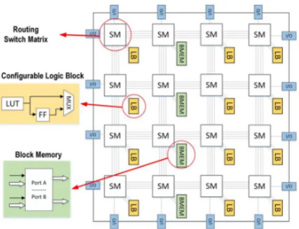
Generally, FPGA architectures are island-style where a wide variety of heterogeneous resources, including logic blocks, on-chip block memories, I/O blocks and DSPs are connected via routing switch boxes (Figure 1). Configuration memory bits
Fig. 1: Distribution of logic blocks, on-chip memory blocks, routing switch matrices, and I/O blocks inside a generic FPGA architecture.
which normally are not directly visible to user, specify how reconfigurable fabric operates. An example for this invisible configuration is the operation of switch boxes, where they need to be set up to provide required connectivity among utilized resources. SRAM-based FPGAs preserve configuration bits inside volatile static memory bits (which are loaded to FPGA every time at power up from an off-chip flash memory), while a different approach is used in flash-based FPGAs, where configuration is stored in none-volatile flash memory bits to achieve less power consumption and more stability. User design is mapped to several configurable logic blocks, each contains a few read-only Look-Up Tables (LUTs) to implement the combinational logic, and a set of user flip-flops (FFs)/latches to implement sequential logic such as registers and state machines. In this setup, user FFs/latches keep the state of user circuit.
Any upset within FPGA configuration memory is especially troublesome since it may change the operation of FPGA. Nevertheless, since FPGA configuration is static and not changing, configuration memory cells can be protected by special techniques to reduce the reliability gap with ASICs. However, state of user design or sequential logic which is inside user FFs are vulnerable similar to ASICS. Adverse extraneous factors like high energy particle strike or noise can corrupt values of FFs. Fortunately, the flexible structure of FPGAs permits using redundancy to bring more protection. 2017 IEEE Computer Society Annual Symposium on VLSI
In this paper, we propose Joint Latch (JLatch) and Joint Flip-Flop (JFF), two novel hardening solutions. Specifically, we implement reconfigurable storage elements that take ad-vantage of the trade-off between FPGA user resource count and fault resilience at a tunable granularity level. JLatch and JFF are two simple low-overhead circuit ideas which join together four pre-selected latches or FFs to make a single but highly robust storage element when reliability becomes a concern (e.g., in harsh environmental conditions). This work is complementary to our previous work [2], which addressed SRAM memories to be used in FPGA’s BRAMs and LUTs (since both have SRAM structure [12], [13]), while the current study addresses user latches and FFs. The main contributions of this study are as follows:
• We implement hardened latch and FF to mitigate soft
errors in FPGAs where reliable mode practically pro-vides full immunity against single event upsets (SEUs). Moreover, it effectively copes with Multiple Bit Upsets (MBUs). Additionally, provided that special transistor sizing is applied (necessary for some latch structures), any single fault is also automatically and instantly corrected.
• Our approach brings reconfigurability of reliability to user
latches and FFs with fine granularity, where it can only be applied to required number of FPGA logic blocks. This technique is particularly useful for reconfigurable fabrics like commercial-grade FPGAs making them more suitable for critical applications.
• JLatch and JFF are somewhat similar to prevalent
hard-ware redundancy techniques like TMR, but without any explicit majority voter at output. Consequently, voter failure is not a concern, and voter delay is not added to the path delay.
II. BACKGROUND ANDRELATEDWORK
In this section, we review some prominent existing solutions concerning reliability enhancement in FPGAs. Historically, hardening solutions for digital circuits are classified into three categories [20]. In Radiation Hardening by Process (RHBP) which we will not discuss in here, hardening is achieved by none-conventional and expensive foundry processes with using special materials. In Radiation Hardening by Design (RHBD), reliability improvement is achieved by using addi-tional transistors, special transistor spacing [7], circuit level redundancy strategies such as DICE [3], etc, for customized none-commercial chips built particularly for critical applica-tions. In such designs, considerable overheads of area, power and performance may be tolerated to achieve necessary relia-bility which make them improper for commercial applications. Moreover, increasing importance of MBU effect has made some of such solutions ineffective [8]. In Radiation Harden-ing by Architecture (RHBA), commercial parts are used in redundant and duplicative configurations (in component level, board level, or system level) to achieve the required level of reliability.
Configuration memory bits, internal block memories, and the state of user circuit inside sequential logic are typical
Fig. 2: A robust SRAM cell [2] implemented by combining four SRAM cells like a ring (bit-lines and access transistors are not shown). When CTRL=1, four cells form a single hardened cell with internal data redundancy.
vulnerable parts of an FPGA. Any fault in configuration results in corruption of FPGA operation (corruption of routings or combinational functions) which mandates correction, for ex-ample by reloading the configuration. In the case of sequential logic, however, fault leads to a change in the state of circuit where a circuit restart may become necessary. Some reliability solutions are specifically applicable to configuration memories, such as storing them on on-chip none-volatile flash memory bits as in the flash-based FPGAs; or scrubbing which means reloading the configuration memory periodically or on demand to overwrite occasional errors [16]. In the case of internal block memories, ECC is a common solution as it can be effectively employed within any regular memory structure. Because user FFs are individual storage cells with changing value, above solutions are not applicable to them.
Studies about protecting FFs are mainly based on redun-dancy techniques such as TMR. Some radiation-hardened FPGAs use three FFs plus a dedicated voter to implement TMR to have a single hardened FF [19]. Xilinx V5QV FPGA [17] is a modified version of commercial-grade Virtex-5 FPGA that incorporates RHBD technology to protect FPGA against SEUs and achieve space qualification. As one can expect, area overhead in RHBD techniques is significant. Xilinx’s TMRTOOL [15], is a tool for automatic conversion of user design into TMR version for protection against radiation in commercial-grade FPGAs. The tool automatically triplicates inputs, logics, and outputs and also inserts majority voters with feedback loops to correct failures without programmer intervention.
In our previous study [2], we proposed a reconfigurable SRAM cell which trades-off reliability and memory size in SRAMs (see Figure 2). Besides other applications such as caches or register files, this technique is also applicable to LUTs and block memories within FPGA. Because both are SRAM-based structures [12], [13]. This work is a comple-mentary study to cover latches and FFs, as well as LUTs and block memories.
Fig. 3: Three typical implementations for static latch. 1) SR latch similar to SRAM cell with special transistor sizing. 2) D latch based on SR NAND latch. 3) D latch by pass transistor logic. Our technique is applicable to all cases.
III. STRUCTURES OFJLATCH ANDJFF
A. Circuit Description
Structure of a static latch is rather similar to SRAM cell, where two cross-coupled inverters hold stable opposite values by feedback loops, ’0’-’1’ or ’1’-’0’. However, access circuitry and transistor sizing in some implementations are quite differ-ent than SRAM cell. Three typical latch implemdiffer-entations are shown in Figure 3. To store a value into a latch, in (1), the value is pushed inside which requires proper transistor sizing, similar to SRAM cell. But, in (2) and (3), to write a new value, the feedback loop is broken by setting the enable input. JLatch technique is applicable to all cases in Figure 3.
JLatch (Joint Latch) is constructed by connecting outputs of four static latches like a ring by means of four joiner switches as depicted in Figure 4. Each joiner connects two internal nodes of two distinct latches to each other, here Q1 to Q2,
Q2 to Q3, Q3 to Q4 and Q4 to Q1. Provided that the joiner
type and size, and the size of latch transistors are appropriately selected, this structure has two stable states: all four latches
Fig. 4: JLatch is a reconfigurable hardened static latch imple-mented by joining outputs of four latches like a ring. When CTRL=1, latch 1, 2, 3, and 4 form a single radiation hardened latch with internal data redundancy, meaningQ1=Q2=Q3=Q4 andQ1=Q2=Q3=Q4.
Fig. 5: JDFF (Joint D Flip-Flop) is built from two JDLatches (Joint D Latches) on the left. This structure provides four separate normal DFF or a single radiation hardened DFF. Conventional TMR technique on the right.
store ’1’ (Qi=’1’, Qi=’0’) or all store ’0’ (Qi=’0’, Qi=’1’). Any other state immediately goes to one of these two stable states. The logic behind this idea is that the coupled nodes which hold redundant values, electrically support each other if any instability threatens either one of them. Each latch receives a direct support from two adjacent ones. For example, latch 1 is supported by latch 2 and latch 4 (Figure 4). In some latch/FF designs a buffer is placed at output. In those cases, the joiner switches should be placed before output buffers to connect internal nodes of feedback loops to each other.
In normal mode, switches (joiners) are off. Therefore, latches 1, 2, 3, and 4 are four separate ones which store independent values without interfering with each other. When reliability becomes a concern, the joiner switches can be turned on (user sets CTRL=1) to join the latches together. In this mode, ring of four latches constructs a single but more robust latch. All four latches keep redundant data values. As typically master-slave FFs are built from two level-sensitive latches, JFF (Joint Flip-Flop) is also built from two JLatches to form one robust FF from four normal FFs. In Figure 5-left, one JDFF (Joint D Flip-Flop) is built from two JDLatches (Joint D latches), where four normal DFFs can be traded-off for having one hardened DFF. This is somehow similar to prevalent hardware redundancy techniques like Triple Modular Redundancy (TMR) as shown in Figure 5-right. This will be discussed later.
B. Joiner Switch and transistor sizing
As discussed in [2], for selecting proper joiner switch, both PMOS and NMOS transistor types with different W/L sizes have to be analyzed. Simulation results show that NMOS has superior performance over PMOS. Moreover, wider transistor provides better connectivity and better mutual support. Mini-mum size of joiner depends on size of latch transistors, but in most of the cases NMOS1 or NMOS2 are enough (NMOSX is X times wider than minimum sized NMOS).
Fig. 6: If CTRL=1, node capacitance and discharging path (for discharging collected charge) of node Q2 is added to node Q1. Traditionally in standard CMOS gate design, pull-up and pull-down networks are sized unbiasedly to have equal high-to-low and low-to-high worst-case delay. On the other hand, SRAM cells require special transistor sizing for proper func-tionality, in which pull-down transistor is around four times stronger (two times wider) than pull-up [1]. As the reason will be explained in auto-correction section, in a similar approach that we had in [2] for SRAMs, our solution requires a biased transistor sizing for the inverters or gates inside feedback loop of static latch. One of the pull-up or pull-down transistors has to be at least two times stronger than the other. The latch (1) in Figure 3 has already such necessary sizing, but for other two, size of transistors inside data retention feedback loop should be adjusted accordingly. In the cases that latch/FF’s biased output voltage is not acceptable, output buffers which are used in many practical designs can solve the issue.
C. Soft-Error Mitigation
Critical charge (Qcrit)—the maximum tolerable amount of collected charge by a particle strike without changing the cell value—is a measure of soft-error sensitivity of circuit nodes. Node capacitance and its charging/discharging time constants (τ), determine value of Qcrit. In JLatch (and JFF), when joiners are active, redundant nodes are coupled to each other. Therefore, capacitance and discharging path of another node is added to the node suffering from a radiation hit (Figure 6). In this way, node capacitance is increased which leads to more stability. Additionally, parallel down (or pull-up) transistors discharge the collected charge faster. Therefore, overall a stronger particle is needed to flip the cell. Simulation shows that depending on static latch structure, the increase in
Qcritis at least three orders of magnitude (1000X). Because of exponential relation betweenQcritand Soft Error Rate (SER) [4], we can practically say this structure is immune against SEUs.
If the four latches to join are in a safe interleaving distance to avoid MBU effect [9], JLatch can withstand against MBUs effectively as well, but obviously with additional wiring cost. Information about dies of existing FPGAs is commercial secrets and not publicly available. However, considering the size of circuits inside a typical FPGA logic block which includes multiple LUTs and multiplexers [13], we expect that a few latches or FFs can easily be interleaved (if are not already) among other resources for having such a safe distance.
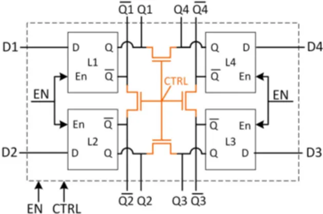
Fig. 7: Auto-correction mechanism in hardened SRAM cell [2] is also applicable to JLatch and JFF, provided that size of transistors are adjusted properly. Assuming ’0’ is stronger than ’1’, a durable fault propagates from latch 1 to 4. Latch 2 and 3 are not affected and later will recover genuine values of latch 1 and 4.
D. Auto-Correction and Fault Immunity
If we assume that faults are still probable inside JLatch structure by any reason, our idea unveils another feature for immediate correction of any single fault. The special transistor sizing explained in section III-B, prevents fault propagation inside the ring of four bits. Later, after disappearance of fault source, faulty bits are recovered instantly. In the first latch in Figure 3, which is similar to standard SRAM cell, sizing is already biased where’0’ is stronger than ’1’. But in most of latch/FF implementations such as the second and third ones in Figure 3, transistor sizings are as normal CMOS gates and not similar to SRAM cell. Hence, the JLatch technique is not directly applicable to these, unless sizing of their pull-up and pull-down networks are adjusted properly. For example, in the scenario in Figure 7, a durable single fault occurs in latch 1 and then it propagates to latch 4, but not to latch 2 and 3. Because weaker ’1’ values in latch 1 and 4 can not dominate stronger ’0’ values in latch 2 and 3. Later, two intact bits push and recover the two faulty bits. Simulation of auto-correction mechanism for SRAM cell is presented in [2] and result is similar to JLatch.
E. Overheads
We expect that timing and area overheads of additional wirings for JLatch/JFF which are limited to be inside logic blocks are negligible. This is due to long routing lines inside FPGA’s complex interconnection network, low operational frequency of reconfigurable fabrics, and relatively small size of logic blocks. This technique requires one (two) extra transis-tor(s) per latch (FF) as shown in Figure 4. For example, Xilinx Virtex UltraScale XCVU440 contains more than 20 billion transistors [18] and around 5 million CLB FFs. Therefore, increase in total transistor count is trivial. Moreover, equipping only some FPGA logic blocks with JLatch/JFF to protect most critical parts of design, such as the processor running diagnostics routines, can reduce the costs. As it had been depicted in Figure 5, JDFF requires an identical data input for
all four FFs. This is done by normal FPGA routing resources, similar to what is done for a typical TMR design.
F. Other Considerations
We assume that in normal mode, when CTRL=0 and the JLatch/JFF technique is not applied, all individual latches and FFs are free of process variation problems. On the other hand, joiner switches are not very sensitive to process variation. If their resistance is low enough, which often is achievable even by minimum size NMOS transistor, they work as intended. This was shown through simulation for different (W/L) tran-sistor sizes in earlier study [2].
In this paper, we consider Latches and FFs (sequential logic) in hold state. We do not consider Single Event Transients (SETs) inside combinational logic which may generate a glitch and then propagated into sequential logic. Although the SETs are not relevant for our current work, our previous study which covered SRAM cells [2] is applicable to LUTs and BRAMs inside FPGA. It not only protects SRAM cell values, but also damps the glitch amplitude originated from them.
IV. SIMULATION
A. Setup
We simulated our technique on Advanced Design System (ADS) with 22nm predictive technology model library [14]. Transistor sizes for all latches of Figure 3 are selected as follows: In all cases L = Lmin. For latch 1,(W/L)P D = (W/L)P U = (W/L)joiner= 1 and (W/L)P G= 2. For latch 2,(W/L)P D = 2 and (W/L)P U = 1 for NAND gate, and (W/L)joiner = 1. For latch 3, (W/L)P D = (W/L)P U = 1 for inverter,(W/L)P D= (W/L)P U = 2 for tri-state inverter and(W/L)joiner= 2.
B. Simulation of SEU
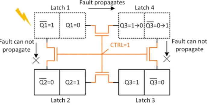
The traditional method for measuringQcrit via simulation, is through injection of current pulse into circuit nodes. In the literature, current pulse with various shapes such as rectangular, triangular, and exponential is used to model SEU. In our simulation setup, as illustrated in Figure 8, we inject rectangular current pulse with variable width and amplitude into victim nodes of latch L1. Two current sources shown in the Figure, either inject a pulse into ’0’ node (Q1), or out of ’1’ node (Q1). We run both cases and consider the worst one. For every pulse width ranging from 0.1 picoseconds to 1 nanoseconds, pulse amplitude is increased up to the point such that the whole JLatch flips. While it is still possible that the injected current pulse corrupts the value of hardened JLatch, the possibility is very low, due to significant increase in requiredQcrit.
Simulations are performed for three latches in Figure 3 and their hardened versions while they are in hold state. In Figure 9, the achieved improvements have been depicted. The y-axis is maximum tolerable amplitude of injected current pulse, for every pulse width on x-axis. For all three cases, the required pulse amplitude (or equivalently required Qcrit, as it is the area under pulse shape) is at least three orders of magnitude
Fig. 8: Particle strike is modeled by current injection into circuit nodes. Both nodes of memory bit are tested while latch is in hold state.
(1000X) larger than what is needed to flip the simple latches. Table I shows theQcritvalues.
TABLE I: Critical charge of normal and proposed joint latches for pulse width=1ns.
L1 L2 L3 JL1 JL2 JL3
Qcrit (fC) 8 18 15 32000 3450000 17000
SER = K × φ × A × exp (−Qcrit
Qs )
(1) Considering critical charge values in Table I, we assume that such extremely high energy particles with this capability are very rare and therefore, we conclude that for realistic scenarios JLatch (and then JFF) is fully immune against any single particle strike while it is in hold state. Equation 1 expresses the SER in terms of Qcrit [4]. The SER by cell decreases exponentially withQcrit and then, according to Qcrit values shown in Table I, the joint latch has a SER that is practically equals to zero, which implies its full immunity against particle strikes. K is a proportionality constant,φ is the neutron flux with energy greater than 1MeV, A is the sensitive area of the
Fig. 9: Improvement achieved by hardening latch implementa-tions of Figure 3. The y-axis is maximum tolerable amplitude of injected current pulse, for every pulse width on x-axis.
circuit andQsis the charge collection efficiency of the device, in fC.
C. Comparison with TMR
In the literature, there are some well-known hardening solu-tions like DICE [3] as discussed in section II. But due to large and fixed overheads, they are only applicable to special and none-commercial products. However, our solution is recon-figurable and applicable to commercial-grade FPGAs. Hence, they are not directly comparable. We compare JLatch/JFF with TMR which is a well-known user-level technique implemented in user’s HDL code.
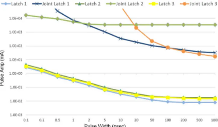
In TMR, unless the majority voter is also replicated (which imposes large overheads), reliability is still a concern due to the voter failure which directly affects the output. However, in JFF, no explicit single point of failure hardware voter exists, thereby eliminating such concerns. Moreover, the delay of voter is not added to critical path like conventional majority voters. In Figure 10, the delay of normal DFF, TMR DFF, and JDFF (as was shown in Figure 5) with implementation of latch 3 (as was shown in Figure 3) are compared for Vdd ranging from 0.5V to 0.9V. Delay is measured as the time between clock edge and the time in which output signal reachesVdd/2 while a minimum size inverter is at output as load. Delay is selected from maximum of low-to-high and high-to-low values. As the simulation results show (see Figure 10), the voting delay is significantly reduced form 50%-80% in the case of TMR DFF, to 10%-20% in the case of JDFF. This is mainly due to the fact that voter is not in series at output as it is the case in usual voting architectures.
V. CONCLUSION
In this work, we propose JLatch and JFF, novel and simple circuit techniques for achieving a flexible trade-off between available resource size (number of user latches and Flip-Flops) and reliability inside FPGAs. With special circuit design, significant improvement in critical charge (Qcrit) is achieved
Fig. 10: Comparison between delay of a normal DFF, a triplicated DFF with a majority voter at output (TMR DFF), and a JDFF. The voter delay is reduced form 50%-80% in TMR DFF, to 10%-20% in JDFF.
to practically bring immunity against SEUs. Moreover, pro-vided that special transistor sizing is applied, JLatch (and JFF) presents a novel self-correcting technique to immediately correct any occurrence of single faults to avoid degradation of redundancy. Additionally, by this technique, the delay of majority voter as it exists in conventional replication tech-niques such as TMR, is significantly reduced. Area overhead for having flexibility of these structures is only one extra transistor per normal static latch (two extra transistors per normal master-slave Flip-Flop).
VI. ACKNOWLEDGMENTS
This research is supported in part by TUBITAK grant 115E835.
REFERENCES
[1] A. Pavlov, M. Sachdev, CMOS SRAM Circuit Design and Parametric Test in Nano-Scaled Technologies. Springer, 2008.
[2] H. Ahangari, G. Yalcin, O. Ozturk, O. Unsal, A. Cristal, ”JSRAM: A Circuit-Level Technique for Trading-Off Robustness and Capacity in Cache Memories”, Proc. ISVLSI, pp. 149-154, 2015.
[3] T. Calin, M. Nicolaidis, R. Velazco, ”Upset hardened memory design for submicron CMOS technology”, IEEE Trans. Nucl. Sci., vol. 43, no. 6, pp. 2874-2878, Dec. 1996.
[4] P. Hazucha, C. Svensson, ”Impact of CMOS Technology Scaling on the Atmospheric Neutron Soft Error Rate”, IEEE Trans. Nuclear Science, vol. 47, pp. 2586-2594, Dec. 2000.
[5] P. Jain, V. Zhu, ”Judicious choice of waveform parameters and accurate estimation of critical charge for logic SER”, Proc. DSN, 2007. [6] I. Kuon, J. Rose, ”Measuring the Gap Between FPGAs and ASICs”, IEEE
Trans. Comput.-Aided Design, vol. 26, no. 2, pp. 203-215, Feb. 2007. [7] H.-H. K. Lee, K. Lilja, M. Bounasser, P. Relangi, I. R. Linscott, U.
S. Inan, S. Mitra, ”LEAP: Layout design through error-aware transistor positioning for soft-error resilient sequential cell design”, IEEE Int. Reliab. Phys. Symp. (IRPS), 2010.
[8] T. D. Loveless, S. Jagannathan, T. Reece, J. Chetia, B. L. Bhuva, M. W. McCurdy, L. W. Massengill, S. J. Wen, R. Wong, D. Rennie, ”Neutron-and proton-induced single event upsets for D- ”Neutron-and DICE-Flip/Flop designs at a 40 nm technology node”, IEEE Trans. Nucl. Sci., vol. 58, no. 3, pp. 1008-1014, Jun. 2011.
[9] P. Reviriego, J. A. Maestro, S. Baeg, S. Wen, R. Wong, ”Protection of memories suffering MCUs through the selection of the optimal interleaving distance”, IEEE Trans. Nucl. Sci., vol. 57, no. 4, Aug. 2010. [10] M. Wirthlin, ”High-reliability FPGA-based systems: Space high-energy physics and beyond”, Proc. IEEE, vol. 103, no. 3, pp. 379-389, Apr. 2015. [11] C. Shin, ”Advanced MOSFET designs and implications for SRAM
scaling,” Ph.D. dissertation, University of California, Berkeley, 2011. [12] R. C. Pang, S. P. Young, T. J. Bauer, ”Block RAM with configurable
data width and parity for use in a field programmable gate array”, U.S. Patent 6 346 825, February 12, 2002.
[13] R. D. Wittig, S. Mohan, R. A. Carberry, ”FPGA configurable logic block with multi-purpose logic/memory circuit”, U.S. Patent 6 150 838, November 21, 2000.
[14] ”Predictive Technology Model for Spice.”, Internet:http://ptm.asu.edu. [15] ”Xilinx TMRTOOL”,www.xilinx.com/ise/optional prod/tmrtool.htm. [16] C. Carmichael, M. Caffrey, and A. Salazar, ”Correcting single-event
upsets through Virtex partial configuration,” Xilinx Corporation, Jun.1, 2000, Tech. report, XAPP216 (v1.0).
[17] ”Radiation-hardened, space-grade Virtex-5qv family overview,” Mar. 2012, DS192 (v1.3).
[18] http://www.xilinx.com/publications/archives/xcell/Xcell86.pdf, First quarter 2014.
[19] J. McCollum, R. Lambertson, J. Ranweera, J. Moriarta, J. J. Want, F. Hawley, and A. Kundu, ”Reliability of antifuse-based field programmable gate arrays for military and aerospace applications”, presented at the MAPLD, Laurel, MD, USA, Sep.1113, 2001, Actel Corporation. [20] A. Keys, J. Adams, R. Darty, and M. Patrick, ”Radiation hardened
elec-tronics for space environments (RHESE) project overview,” International Planetary Probes Workshop, NASA, Atlanta, GA, 2008.
![Fig. 2: A robust SRAM cell [2] implemented by combining four SRAM cells like a ring (bit-lines and access transistors are not shown)](https://thumb-eu.123doks.com/thumbv2/9libnet/5987573.125654/2.918.530.773.105.334/robust-sram-implemented-combining-sram-cells-access-transistors.webp)