Layer-by-layer photonic crystals from microwave
to far-infrared frequencies
E. O¨ zbay
Department of Physics, Bilkent University, Bilkent, Ankara 06533, Turkey
Received November 3, 1995; revised manuscript received March 28, 1996
The use of layer-by-layer geometry to build photonic band-gap crystals at various frequencies ranging from microwave to the far-infrared is described. The layer-by-layer structure yields a full photonic band gap in all directions, and this is experimentally confirmed at microwave frequencies. The structures are then built at smaller scales by means of silicon micromachining with photonic band-gap frequencies as high as 500 GHz. Transmission characteristics and the reflection characteristics of the millimeter-wave photonic crystals are re-ported. The use of laser-micromachined alumina substrates to build three-dimensional millimeter-wave pho-tonic crystals is also described. Defect structures are investigated at microwave and millimeter-wave fre-quencies. © 1996 Optical Society of America.
1. INTRODUCTION
In analogy to that of electrons in a crystal, the propaga-tion of electromagnetic (EM) waves in a three-dimensional dielectric structure can be forbidden for a certain range of frequencies. These three-dimensional structures, which are called photonic band-gap (PBG) crystals, have recently received both theoretical and ex-perimental attention.1–6 The initial interest in this sub-ject came from a proposal to use PBG crystals to inhibit spontaneous emission in photonic devices, leading to more-efficient light emitters such as thresholdless semi-conductor lasers7,8 and single-mode light-emitting diodes.9,10 The proposed applications were later
ex-tended to the millimeter- and submillimeter-wave re-gimes and included efficient antennas, sources, waveguides, and other components that take advantage of the unique properties of PBG materials.11–14
However, the difficulties associated with the fabrica-tion of smaller-scale structures have restricted the experi-mental demonstration of the basic PBG crystals to micro-wave frequencies (12–15 GHz).15 Although there are continuing efforts to use reactive ion-beam etching tech-niques to leapfrog the frequency performance to optical frequencies,16to my knowledge these efforts have not yet produced photonic crystals with a full band gap at optical frequencies. Besides, reactive ion-beam etching tech-niques are not practical for fabricating photonic crystals at far-infrared or submillimeter wave frequencies. The thickness of the dielectric material to be etched away can be of the order of a few millimeters, too thick for such etching schemes. Besides three-dimensional structures, two-dimensional triangular lattices of dielectric rods or of air columns in a dielectric material have also been fabri-cated that reveal two-dimensional PBG’s that agree well with photonic band structure calculations.17 However, in these structures EM waves can propagate freely in the di-rection parallel to the rods. So there is a genuine need for photonic structures with full PBG’s in all directions that can be built at a wide range of frequencies. In this
paper, I describe the properties of layer-by-layer photonic crystals at frequencies ranging from microwave to the far infrared.
2. STRUCTURE
The layer-by-layer PBG crystal consists of simple one-dimensional dielectric rods as the basic building blocks [Fig. 1(a)]. The structure is assembled by stacking layers of dielectric rods, with each layer consisting of parallel rods with a center-to-center separation of a. The rods are rotated 90° in each successive layer. Starting at any reference layer, the rods of every second neighboring layer are parallel to the reference layer but shifted a dis-tance of 0.5a perpendicular to the rod axes. This results in a stacking sequence that repeats every four layers. This lattice has face-centered tetragonal lattice symmetry with a basis of two rods. The PBG is not sensitive to the cross-sectional shape of the rods. This structure has a PBG when both the filling ratio and the dielectric contrast meet certain requirements.18
We define the plane of each rod layer as the x – y plane with the rod axes defining the (110) directions in this plane. Figure 1(b) shows the corresponding first Bril-louin zone of the photonic crystal, which has face-centered tetragonal symmetry. The symmetry of this crystal is such that the EM wave propagation along the z axis is de-generate for both polarizations. However, for propaga-tion along the rods (110 direcpropaga-tion) the propagapropaga-tion for the polarization vector e1in the x – y plane is nondegenerate,
with e2along the z axis [Fig. 1(c)]. Another propagation
direction that is of interest is also described in Fig. 1(c), where the propagation direction is at an incident angleu to the surface normal while the polarization vector e3is
still parallel to the surface. Foru 5 0 the propagation is along the stacking direction.
3. MICROWAVE CRYSTALS
The transmission and phase dispersion properties of the microwave regime structures were measured with a
Hewlett-Packard 8510A network analyzer. Standard gain horn antennas were used to transmit and receive the EM radiation. Surroundings of the test setup were cov-ered with absorbers to build an anechoic chamber,
result-ing in a sensitivity of 70 dB. The setup was calibrated for phase and power measurements of the EM wave transmitted between the antennas. The structure was placed in the beam path of the EM wave transmitted from the source antenna. Additional absorbers were used to surround the side faces of the structure to minimize the leakage caused by surface states. Two separate pairs of antennas were used to cover the 6–20-GHz measurement range. Propagation characteristics along the z axis were obtained by facing the top surface (x – y plane) of the structure to the source antenna. Propagation along the (110) direction was obtained by facing the side surfaces of the structure to the source antenna. Different polariza-tions were achieved by rotating the antennas 90°.
In the microwave frequency regime the new photonic crystal can be built with commercially available alumina rods with a refractive index of 3.1. Three different crys-tals were constructed in this frequency range. The first crystal was built with cylindrical alumina rods 0.31 cm in diameter and 15.24 cm long. A center-to-center separa-tion of 1.12 cm was chosen to yield a dielectric filling ratio of ;0.26. The photonic gaps of the crystal for propaga-tion along major axes were determined by transmission measurements (which were reported in Ref. 19). A stop band was measured along the stacking direction from
Fig. 1. (a) Schematic depicting the basic structure of the new PBG crystal. The structure repeats every four layers in the stacking direction. (b) First Brillouin zone of the photonic gap structure, which carries a face-centered tetragonal symmetry. The^001& direction corresponds to propagation along the stack-ing direction. The ^011& direction corresponds to propagation along the rod axes. (c) Pictorial description of the propagation of electromagnetic waves along the rods with the polarization e1
vector parallel to the z axis, the polarization vector e2parallel to the x – y plane and at an incidence angle to the surface normal, and the polarization vector e3parallel to the top surface.
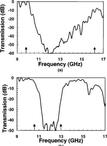
Fig. 2. (a) Transmission characteristics of the second microwave photonic crystal along the stacking direction (z axis). There is no e-field polarization dependence for this propagation direction. (b) Transmission characteristics of the photonic gap structure along the x axis when the e field is perpendicular to the rods. The arrows show the calculated positions of band edges in both plots.
10.7 to 17.4 GHz. The calculated band-gap edges for this propagation were 11.1 and 16.8 GHz. For propagation along the rods with the polarization vector e along the z axis [see Fig. 1(c)] the lower edge of the photonic gap oc-curred at 11.9 GHz, and the upper edge was at 14.0 GHz. This is very close to the calculated band-gap edges of 11.7 and 13.7 GHz. The experimental gap frequencies along several directions were in excellent agreement with the calculated gap values. The first Brillouin zone was also mapped, and the structure was found to have a full band gap between 11.7 and 13.5 GHz.20
As mentioned above, the theoretical simulations pre-dicted that the PBG was not sensitive to the cross-sectional shape of the rods. So one would expect to ob-tain a full PBG with similar properties from structures made of rods with different cross sections. To test this argument a second crystal was constructed; this time square-shaped rods (0.32 cm3 0.32 cm 3 15.24 cm) were used instead of the cylindrical-shaped rods used for the first crystal. The design was kept similar to that of the first crystal, for which a center-to-center separation of 1.12 cm, corresponding to a dielectric filling ratio of;0.29 was chosen. Figure 2(a) shows the transmission charac-teristics of the propagation along the z axis for a structure with four unit cells along the z axis. The lower edge of the gap starts at 10.0 GHz, and the upper edge is;16.2 GHz. Figure 2(b) shows the transmission measurement for propagation along the rods with the polarization vec-tor e along the z axis. The lower edge of the photonic gap is at 10.6 GHz, and the upper edge is at 13.0 GHz. The corresponding band-edge frequencies of the second crystal were lower than those of the first crystal. This was ex-pected, as the second crystal had a higher dielectric filling ratio than the first crystal. These band-gap edge values, along with those of the stop bands, were measured along
other directions and found to be close to the theoretical calculations, which predicted a full band gap from 10.6 to 12.7 GHz. This corresponded to a band-gap-to-mid-gap ratio of 18%, which is theoretically the maximum attain-able band-gap-to-mid-gap ratio from square-shaped alu-mina rod photonic crystals.18
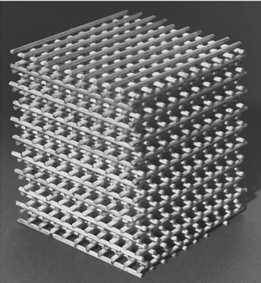
The third microwave crystal was made of relatively thinner cylindrical rods (0.31 cm in diameter and 7.5 cm long). The center-to-center separation of the rods was chosen to be 0.75 cm. A photograph of this crystal is shown in Fig. 3. This crystal was used to check the po-larization dependence of the transmission along the x – y axis. Figure 4(a) shows the transmission characteristics of the crystal along the rods with the polarization vector e along the z axis. The lower edge of the photonic gap is at 18 GHz, and the upper edge is at 22 GHz, in good agree-ment with theoretical predictions of 18.3 and 21.4 GHz. For this propagation direction my theoretical simulations predicted that the transmission would be different for each different polarization. To check this prediction, the polarization was changed by rotating the standard-gain horn antennas by 90° while keeping the same propaga-tion direcpropaga-tion. Figure 4(b) shows the transmission prop-erties along the same direction, with polarization vector e perpendicular to the z axis. For this polarization the lower edge starts from 17.0 GHz and the upper edge is ;22.0 GHz. The theoretical prediction for the lower edge
Fig. 3. Photograph of the second microwave crystal made of cy-lindrical alumina rods.
Fig. 4. Transmission characteristics of the third microwave crystal for propagation along the rods where polarization vector is (a) perpendicular to the rods, (b) parallel to the rods. The ar-rows show the calculated positions of band edges in both plots.
was 18.3 GHz, in good agreement with the experiment. But for the upper edge the agreement did not hold: The theory predicted an upper edge of 24.1 GHz, which was much higher than the experimental upper edge of 22.0 GHz. As the experimental upper edges of both measure-ments were very close to each other, this phenomenon could be explained by the coupling of the incident EM waves to the conduction band with the reverse polariza-tion.
4. MILLIMETER-WAVE CRYSTALS
Silicon micromachining methods were used to scale down the layer-by-layer structure to smaller dimensions. This method utilizes the anisotropic etching of silicon by aque-ous potassium hydroxide (KOH), which etches the $110% planes of silicon rapidly while leaving the $111% planes relatively untouched. Thus by use of (110)-oriented sili-con it is possible to etch arrays of parallel rods into wa-fers, and the patterned wafers can then be stacked in the correct manner to make the PBG crystal.
The (110) silicon wafers used in this research were each 7.62 cm in diameter and 390 mm thick. The fabrication was carried out with batches of 20 wafers. The first step in the process was the growth of silicon dioxide on the front and back surfaces of the wafers. The oxide must serve as a mask during the anisotropic etching step, and a 2.0-mm-thick oxide was sufficient to provide the necessary protection. After oxidation, the front-surface oxide was patterned by conventional photolithography and buffered hydrofluoric acid etching. The pattern consisted of 23 parallel stripes, each 340mm wide, separated by 935-mm-wide gaps. These stripe dimensions and the wafer thick-ness determined the center of the forbidden photonic gap, calculated to be 94 GHz in this case. The stripes were aligned parallel to the $111% plane of the silicon, as de-fined by the major flat of the wafer. The stripes were 3.0 cm long, so the 23 stripes formed a square 3.0 cm33.0 cm pattern. A 1.15-cm-wide border around the stripe array was protected by photoresist, with the outer regions of the wafer left exposed so a square wafer would be left after etching. Within the border region were four small rect-angular openings that would serve as guide holes for the stacking process. A layer of photoresist protected the back surface oxide during patterning of the front surface. After the oxide layer was patterned, the wafers were dipped into an aqueous KOH etching solution. A typical etch performed in a 20% KOH solution at a temperature of 85 °C took approximately 4 h to etch entirely through the wafer. Once the etch was completed, the remaining oxide was removed from both surfaces. The individual wafers were stacked to form the photonic crystal by use of a holder that had pins to align to the guide holes that were etched into the wafers. The guide holes were not symmetric with respect to the stripe patterns but instead were offset slightly in the direction perpendicular to the rods. The separation between the edge of the rod pattern and the guide holes on one side was larger than the cor-responding separation on the other side by one half of the rod-to-rod spacing. Thus, if one wafer was rotated by 180° with respect to a second wafer while the guide holes were kept aligned, the rods of first wafer were translated
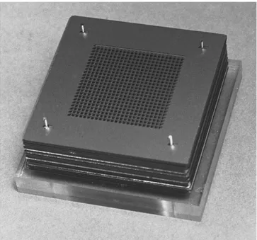
by one half of the rod spacing with respect to the rods of the second wafer. It was then easy to assemble the pho-tonic crystal by stacking the patterned silicon wafers one-by-one on the holder, with a rotation of the holder by 90° before each wafer was put into place. This resulted in a stacking sequence that repeats every four layers, as shown in Fig. 1. A photograph of the stacked silicon mi-cromachined wafers is shown in Fig. 5.
Once the fabrication was completed, the transmission properties of the crystal were measured with a W band (75–110-GHz) measurement arrangement. A Ku-band (12–18 GHz) frequency synthesizer was used to generate a signal that was first amplified and then multiplied in frequency by six times to reach the W band frequency. The high-frequency signal was radiated by a standard-gain horn antenna (aperture size 1.17 cm3 1.45 cm) with the photonic crystal in the path of the beam, and the transmitted radiation was collected by a second horn an-tenna. The amplitude of the received signal was mea-sured by a harmonic mixer and a network analyzer. The setup was calibrated for power measurements of the EM wave transmitted from the source antenna. To improve the sensitivity of the test setup, EM absorbing pads were stacked around the test set to create a pseudoanechoic en-vironment. The typical resulting sensitivity was;60 dB throughout the W band.
In the first millimeter-wave crystal 7.62-cm silicon wa-fers with a resistivity of 30 V cm21were used. Figure 6(a) shows the transmission measurement for propaga-tion along the stacking direcpropaga-tion (normal to the silicon wafer surfaces) of this crystal, which has 28 stacked sili-con wafers (7 unit cells). The drop-off in transmitted power, corresponding to the valence band edge for the crystal, starts near 81 GHz, which matches the calculated value exactly. The upper band edge for this orientation, predicted to be at 120 GHz, was beyond the upper mea-suring limit of the W-band test set and so does not appear in Fig. 6(a). In the forbidden band the average
attenua-Fig. 5. Photograph of the millimeter-wave PBG crystal built by stacking 16 micromachined silicon wafers.
tion was 60 dB, a limit that was most likely due to leak-age of the EM power around the sample, either through surface states of the crystal or through other leakage paths around the crystal. The upper band edge was de-tected when the crystal was rotated so that the EM wave was incident at an angle of 35° with respect to the wafer surface normal [see Fig. 1(c) for a pictorial description of this propagation direction]. Then the complete band gap fell within the measurement range of the experiment, and both edges of the band gap were well defined, as shown in Fig. 6(b). The valence band edge occurred at 76 GHz, and the conduction band edge was at 116 GHz, values that are in good agreement with the calculated values of 79 and 117 GHz.
The transmission characteristics for the case when the EM waves are incident upon the side surface of a silicon wafer stack were then measured. But the expected band-gap characteristics were not observed for this propa-gation; instead an almost flat transmission 40 dB below the incident signal level was measured. This can be ex-plained by the free-carrier absorption of the silicon wa-fers. As can be seen from the photograph (Fig. 5), for a propagation direction along the wafers the EM waves first had to propagate a distance of 1.15 cm before reaching the photonic part of the crystal. After leaving the photonic part, the EM waves had to propagate another 1.15 cm be-fore leaving the crystal. So for a propagation along this
direction the millimeter wave beams have to propagate a total distance of 2.3 cm in bulk silicon with a resistivity of 30V cm. Bulk silicon attenuation can be calculated as21
a 5 v
A
mere0X
1 2HF
1 1S
1 rvere0D
2G
1/2 2 1J
C
1/2 , (1) wherea is the free-carrier absorption, m is the permeabil-ity of free space (4p 3 1027H/m), r is the silicon wafer resistivity, e0 is the free-space dielectric constant(8.8543 10214F/cm),er is the silicon dielectric constant, which is equal to 11.6 at W-band frequencies, and v 5 2pf is the angular frequency. When Eq. (1) is evalu-ated for W-band frequencies a typical attenuation rate of 16 dB/cm is attained for the bulk silicon with a resistivity of 30V cm. So, for a total distance of 2.3 cm, EM waves are attenuated 37 dB within the nonphotonic part of the crystal. This attenuation, along with the reflectance loss of 3.0 dB that arises from the air–dielectric interfaces, ex-plains the 40-dB loss measured through the W-band fre-quencies. Free-carrier absorption can also be used to ex-plain the relatively low transmission (210 dB) values measured for the conduction and valence bands in Fig. 6. To minimize the free-carrier absorption problem, a sec-ond crystal was fabricated by use of silicon wafers with a typical resistivity of 180V cm, and its propagation char-acteristics at W-band frequencies were measured.22 Fig-ure 7(a) shows the propagation characteristics [similar to
Fig. 6. (a) EM wave transmission through the first microma-chined crystal along the stacking direction. The arrows indicate the calculated band-edge frequencies. (b) Transmission charac-teristics when the crystal is rotated 35°.
Fig. 7. (a) EM wave transmission through the second microma-chined crystal when the crystal is rotated 35°. (b) Transmission characteristics for the propagation parallel to the surfaces.
those used for Fig. 6(b)] when the crystal was rotated 35° with respect to the wafer surface normal. The peak transmission for both conduction and valence bands was only 5 dB below the incident signal, which was better than the transmission obtained from the first crystal. For the second crystal the free-carrier absorption was less than that of the first crystal, and the transmission prop-erties along the wafers could be measured because the to-tal expected attenuation would be;15 dB below the inci-dent signal. Figure 7(b) shows the transmission characteristics of the second crystal for the case when the EM waves were incident upon the side surface of a 40-wafer stack, with the electric field polarized perpendicu-lar to the wafer surfaces. The lower edge of the gap was near 87 GHz, and the upper edge was near 110 GHz. These values compare well with those of the calculated band edges of 85 and 107 GHz. The average transmis-sion within the band gap was;45 dB below the incident signal, mostly because of the leakage of the EM power around the crystal. For EM propagation in the stacking direction, the band-gap attenuation was measured as a function of number of stacked unit cells. The result was an average of 16-dB attenuation per unit cell, close to theoretical expectation of 17 dB per unit cell. This result is especially important for device considerations of these structures because three unit cells (for a total of twelve wafers) will yield a PBG with 45–50-dB attenuation, which is large enough for most applications.
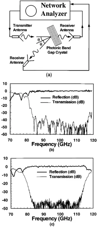
Besides the transmission properties of the photonic crystals, the reflection properties of the millimeter-wave crystals were also measured. Figure 8(a) shows a sche-matic of the reflection measurement setup. Two sepa-rate antennas were used to transmit and receive the EM waves. By changing the location of the receiver antenna back and forth one can measure both the transmitted and the reflected waves. For reflection measurements a metal sheet was used to calibrate the measurements; the metal sheet was assumed to be a 100% reflector at these frequencies. Changing the incidence angle u yields the reflection and transmission properties of the photonic crystals at different propagation directions.
With this measurement setup, the characteristics of the silicon micromachined photonic crystals (which were made of 180 V cm wafers) were measured. Figure 8(b) shows the reflection and transmission characteristics of a 16-layer crystal where u 5 20°. The predicted upper edge was near 120 GHz, which could not be measured with this setup. The band-gap region was 84–119 GHz, and the crystal acted as a perfect mirror for this fre-quency band where 100% of the EM waves were reflected back from the surface of the crystal. For the low-pass re-gion (70–84 GHz) the EM waves were both transmitted and reflected. Figure 8(c) shows the characteristics of the same crystal for an incidence angle of 45°. Both edges of the photonic band gap were measured for this propagation direction. Within the band-gap region (80– 114 GHz) the EM waves were again 100% reflected. For the low-pass region and especially for the high-pass gion one can notice that the total power measured for re-flected and transmitted waves did not add up to 100%. This was explained by the weak coupling of the EM waves to the valence and conduction bands of the crystal, where
the incident radiation at high-pass frequencies was being coupled either to surface modes or to other modes that moved the incident beam away from the receiver antenna.
4. FAR-INFRARED CRYSTALS
One can change the frequency range of silicon microma-chined photonic crystals by simply scaling all dimensions of the structure. The 100-GHz crystals were built with
Fig. 8. (a) Experimental setup for measuring the reflection and transmission properties of the photonic crystals. (b), (c) Reflec-tion and transmission characteristics of the 100-GHz silicon mi-cromachined photonic crystal: (b) for an incidence angle of 20°, (c) for an incidence angle of 45°.
readily available wafers with a thickness of 390mm. To extend this performance to submillimeter waves or to the far-infrared regime one needs to use custom-made ultra-thin silicon (110) wafers. With the theoretical simulation tools, a 500-GHz crystal was designed around 100 mm-thick silicon (110) wafers.
To build the 500-GHz crystal, fabrication techniques similar to the one used to build 100-GHz crystals were used. Fabrication again consisted of defining stripes that were parallel to (111) planes and subsequently etching the wafers in a KOH etch solution. The aforementioned anisotropic etching properties of aqueous KOH etch solu-tions resulted in parallel rods with rectangular cross sec-tions, similar to one of the single layers described in Fig. 1(a). The fabricated stripes were 2.0 cm long and 50mm wide, separated by 185-mm-wide gaps. A total of 86 par-allel stripes were fabricated on each wafer, resulting in a square 2.0 cm3 2.0 cm pattern. By use of a holder with pins that aligned the guide holes that were etched through the wafers, the individual etched wafers were then stacked to form the photonic crystal. The (110) sili-con wafers used in this research were each 5.08 cm in di-ameter and 1006 5 mm thick. Relatively high-resistivity wafers (.100 V cm21) were chosen to minimize absorption losses in the silicon. During the course of fab-rication, caution was used in handling the thin silicon
wa-fers, which were susceptible to breakage. A layer of ox-ide, used to protect the back surface of the silicon wafer during the KOH etch, was intentionally kept after the etch. This gave a robust support to the relatively long stripes, preventing individual stripes from bending and bonding to the adjacent stripes.23
Testing was performed with a terahertz free-space spectroscopy setup, shown in Fig. 9 (a).24 The dynamic
range of the system was;30 dB for frequencies up to 550 GHz. A structure consisting of 16 stacked silicon wafers (corresponding to 4 unit cells) was used for transmission measurements. I obtained the characteristics along the stacking direction by placing the structure on the beam path, so the transient radiation propagated in a plane perpendicular to the top surface of the structure. Figure 9(b) shows the transmission characteristics of the propa-gation along the stacking direction. The lower edge of the photonic gap is at 370 GHz, and the upper edge is at 520 GHz. This is very close to the calculated band-gap edges of 378 and 518 GHz. The average measured at-tenuation within the band-gap was ;30 dB, limited by the dynamic range of the experimental setup. The calcu-lations for the band-gap frequencies predicted the attenu-ation to be;65 dB. Although I was able to measure the properties of the PBG only along the stacking direction, my theoretical calculations predicted a full three-dimensional band gap from 425 GHz (which occurs when the sample is rotated 55°) to 518 GHz (which occurs along the stacking direction). By using special silicon thinning methods and double etching25 the wafers on both sur-faces, I believe that the frequency range of this fabrica-tion technology could be extended to build structures with photonic band gaps as high as 3 THz.
5. LASER MICROMACHINED ALUMINA
CRYSTALS
Besides silicon micromachining, laser micromachining methods to build the layer-by-layer photonic crystals was also investigated. Alumina substrates were used for this micromachining method. The square-shaped alumina wafers (Kyocera 96% alumina; resistivity.1010V cm, re-fractive index 2.86 at 100 GHz) used in this study were each 5.1 cm3 5.1 cm by 400mm thick. Using these wa-fers, I built two different crystals with different filling ra-tios. The pattern for the first crystal consisted of 34 par-allel stripes, each 460 mm wide, separated by 460-mm wide gaps for a filling ratio of 50%. These stripe dimen-sions and the wafer thickness determine the center of the forbidden photonic gap, calculated to be 98.8 GHz in this case. The stripes are 3.1 cm long, so the 34 stripes form a square 3.1 cm3 3.1 cm pattern. The stripes are cut with a high-power carbon dioxide laser. A photograph of the laser micromachined alumina wafer along with a stacked photonic crystal can be seen in Fig. 10.
The laser-machined wafers were then stacked to form the first photonic crystal by use of a holder with pins that aligned the guide holes that were machined through the alumina wafers. With a W-band network analyzer, the transmission characteristics of the first crystal are mea-sured. Figure 11(a) shows the transmission measure-ments of a crystal made of 20 layers (or 5 unit cells). The
Fig. 9. (a) Diagram of the all-electronic terahertz free-space spectroscopy system. (b) EM wave transmission through the micromachined crystal in which the wave vector of the incident radiation is normal to the wafer surfaces. The arrows indicate calculated band-edge frequencies.
band gap along the stacking direction was measured to be 80–110 GHz, in relatively good agreement with the theo-retically predicted band-gap edges of 81 and 104 GHz. The attenuation was also measured as a function of num-ber of unit cells. As shown in Fig. 11(b), an average of 7.5 dB per unit cell attenuation from the first photonic crystal was obtained.
As it was not certain whether the alumina wafers would survive the laser machining process, the design of
the first laser-machined alumina photonic crystal was kept conservative by choice of a high dielectric filling ra-tio. The calculated band-gap-to-mid-gap ratio was 7% (compared with 15% for the silicon micromachined crys-tal), which resulted in poor attenuation per unit cell com-pared with that of the silicon micromachined photonic crystals. To increase the band-gap performance to a level closer to the silicon-based crystals, I decided to build a second crystal with a lower dielectric filling ratio.
Square-based alumina wafers with properties similar to those of the wafers used to build the first crystal were again used. The pattern for the second crystal consisted of 24 parallel stripes, each 460 mm wide, separated by 840-mm-wide gaps for a filling ratio of 36%. Theoretical calculations predicted a full band gap from 89.6 to 99.8 GHz, which corresponded to an 11% band-gap-to-mid-gap ratio.
For propagation along the stacking direction, the lower edge of the photonic gap occurred at 85 GHz, whereas the conduction band was beyond the measurement limit of the experimental set up. Figure 12(a) shows the trans-mission characteristics obtained when the EM waves were incident at the front surface of the crystal with an incidence angle of 45° [as described in Fig. 1(c)]. For such a propagation direction, the band gap fell within the measurement limits of the experimental setup. The
va-Fig. 10. Photographs of a laser micromachined alumina wafer and of a stacked crystal.
Fig. 11. (a) Transmission characteristics of the first laser-micro-machined crystal along the stacking direction. (b) Comparison of experimental and theoretical attenuation along the stacking di-rection as a function of number of stacked unit cells. The ar-rows in (a) indicate the calculated band-edge frequencies.
Fig. 12. (a) EM wave transmission through the micromachined crystal when the crystal is rotated 45°. The arrows indicate the calculated band-edge frequencies. (b) Comparison of experi-mental and theoretical attenuation along the stacking direction as a function of number of stacked unit cells.
lence band edge occurred at 80 GHz, and the conduction band edge was at 108 GHz. This was in good agreement with the calculated band-gap edges of 82.2 and 104.8 GHz. The attenuation per unit cell characteristics of the second crystal was also measured. As shown in Fig. 12(b), the agreement between theory (16 dB per unit cell) and experiment (15.5 dB per unit cell) was very good up to the experimental noise level. The attenuation per unit cell for the second laser-micromachined photonic crystal was higher than that of the first laser-machined crystal. The drastic change of the attenuation per unit cell as a function of filling factor also shows the importance of the theoretical tools for designing high-performance photonic crystals. The attenuation per unit cell performance ob-tained from the second crystal was very close to the per-formance obtained from the silicon-based photonic crys-tals. This makes the laser-micromachined alumina photonic crystals a good alternative to silicon-micromachined photonic crystals for certain millimeter wavelength applications, which require minimal absorp-tion of the EM waves within the dielectric material.
6. MICROWAVE DEFECT STRUCTURES
The frequency range of the aforementioned photonic crys-tals is suitable for a number of millimeter- and submillimeter-wave applications, including efficient millimeter-wave antennas, filters, sources, and waveguides.26 However, most of these applications are based on the presence of defect or cavity modes, which one obtains by locally disturbing the periodicity of the photo-nic crystal.27 The frequencies of these modes lie within the forbidden band gap of the pure crystal, and the asso-ciated fields are localized around the defect.In this investigation of defect structures I followed the approach of Yablonovitch et al.,27wherein either portions of the dielectric lattice are removed or extra dielectric ma-terials are inserted into the air gaps. I first investigated the properties of the defects generated at microwave fre-quencies. For this purpose I used the first of the three photonic crystals mentioned earlier in this paper, which exhibited a full three-dimensional band gap between 11.7 and 13.5 GHz.
The defect structure was formed by removal of a por-tion of a single rod. The length of the missing section is
d, and to facilitate possible comparison with similar PBG
crystals with different lattice constants we define the de-fect volume ratio d/a, where a is the center-to-center separation between rods of the PBG crystal. Figure 13(a) shows the transmission characteristics of propagation along the z axis (the stacking direction) for a structure with 4 unit cells (16 layers) along the z axis. The defect was placed at the eighth layer of the structure and had a
d/a ratio of 1. The electric field polarization vector of the
incident EM wave e was parallel to the rods of the defect layer. The defect transmission was centered at 12.85 GHz, and the peak transmission was 30 dB below the in-cident signal. Using an expanded frequency scale, I mea-sured the Q factor (quality factor, defined as the center frequency divided by the peak’s full width at half-maximum) of the peak to be greater than 1000. It was also found that the transmission via the defect was
polar-ization dependent: No defect mode was present when e was perpendicular to the rods of the defect layer.
The transfer-matrix method was used to calculate the EM transmission through a photonic crystal with defects.19,28 Because the transfer-matrix method re-quires periodicity in the directions parallel to the inter-faces, I examined the case of a periodic defect, made by removing every other rod from a single layer. The ex-periments are done with a structure consisting of 4 unit cells (16 layers), where the 8th layer is chosen as the
de-Fig. 13. (a) Transmission characteristics (along the stacking di-rection) obtained from a defect structure with a d/a ratio of 1. (b) Comparison of the theoretical (dashed curve) and experimen-tal (solid curve) transmission characteristics of the periodic de-fect structure. (c) Transmission characteristics (along the stack-ing direction of the second microwave crystal) obtained from a defect structure with a d/a ratio of 1.
fect layer. Figure 13(b) compares the predicted theoreti-cal transmission with the experimental results. As can be seen, the agreement between theory and experiment is especially good for the defect frequency. The measured defect frequency is 12.62 GHz, and theory predicts 12.58 GHz. Although the measured Q factor (750) of the cavity mode is very close to the theoretical Q factor (800), the measured peak transmission of 217 dB is far below the predicted value of 24 dB. The discrepancy is probably due to the finite length of the rods of the test structure, whereas the theoretical calculations assumed a crystal made of infinitely long rods. The theoretical Q factor in-creases rapidly for increasing thickness of the PBG crys-tal. For a structure with 8 unit cells (32 layers), where the defect layer structure is chosen as the 16th layer, cal-culations predict a defect frequency at 12.61 GHz with a
Q factor greater than 1.43 106. This suggests the pos-sibility of building cavity structures with very high Q fac-tors from this geometry. Defect structures created by adding material into the crystal have also been measured, and these experiments compared well with the theoretical calculations.29
Defects generated around the second microwave crystal (which was made by use of square-shaped rods) also yielded cavity structures with properties similar to those of the first crystal. Figure 13(c) shows the transmission characteristics along the stacking direction for a defect structure. The structure was made with 4 unit cells (16 layers), and the defect was again placed at the 8th layer of the structure and had a d/a ratio of 1. The defect mission was centered at 11.98 GHz, and the peak trans-mission was 27 dB below the incident signal, with a Q fac-tor of 1200.
7. MILLIMETER-WAVE DEFECT
STRUCTURES
In these investigations of defects in millimeter-wave structures I looked at defects incorporated into both silicon-micromachined and laser-micromachined alumina structures. Figure 14(a) shows the transmission charac-teristics of a silicon-based millimeter-wave defect struc-ture along the stacking direction. The structure was made with 16 layers of silicon (4 unit cells), and the defect was placed at the 8th layer and had a d/a ratio of 24, which corresponds to a missing rod. The defect was cen-tered around 100 GHz, and the peak transmission of the defect mode was 25 dB below the incident signal, with a Q factor of 250.
I also fabricated defect structures by removing material from the laser-machined alumina crystal, which had a filling ratio of 38%.30 To compare the alumina-based de-fects with silicon-based dede-fects, I again built a four-unit cell structure in which the eighth layer is the defect layer. The defect consisted of a single missing rod, which again corresponded to a d/a ratio of 24. Figure 14(b) shows the transmission properties of this defect structure. The de-fect frequency was centered at 98.6 GHz and had a peak transmission of 10 dB (compared with 25 dB for the sili-con defect) below the incident signal. The Q factor of the defect was measured to be ;1000, which was four times higher than that of the silicon-based defect.
Although silicon micromachining has proved to be suc-cessful for building three-dimensional photonic crystals, it was found that defects incorporated into the silicon-based structures studied here had relatively poor quali-ties compared with those of alumina-based defect struc-tures. I attribute these effects to the relatively low resistivity of the silicon wafers used (180 V cm21) com-pared with that of alumina, which is typically six orders of magnitude larger than the resistivity of silicon. The calculations of the present study show that the transmis-sion at the top of the defect peak and the Q-factor de-crease drastically as one inde-creases the conductivity of the silicon wafers. These results suggest that alumina would be a better dielectric material to use in building high-Q cavity structures for millimeter-wave applica-tions.
8. CONCLUSION
In this paper, I have described the properties of layer-by-layer photonic crystals at a wide range of frequencies from microwave to the far infrared. In the microwave re-gime three different crystals made of alumina rods were measured. In the millimeter-wave regime microma-chined silicon wafers and laser-micromamicroma-chined alumina
Fig. 14. (a) Transmission characteristics (along the stacking di-rection) of a silicon-based millimeter-wave defect structure with a d/a ratio of 24. (b) Transmission characteristics (along the stacking direction) obtained from a laser-micromachined alu-mina defect structure with a d/a ratio of 24.
wafers were used to demonstrate photonic band-gap fre-quencies near 100 GHz. In the far-infrared regime I was able to demonstrate a 500-GHz photonic band-gap fre-quency performance, using ultra-thin micromachined-silicon wafers. Besides the transmission properties of the layer-by-layer crystals, the reflection properties of the crystals at different incident angles were also reported. The measurements in this study showed that the struc-tures act as perfect mirrors with 100% reflection for fre-quencies within the band-gap region. Defects built at microwave frequencies yielded high peak magnitudes along with high quality factors. Alumina was found to be a better dielectric than silicon for building photonic crys-tals and defect structures at millimeter-wave frequencies. In general, the theoretical predictions made here were in good agreement with the experimental results. Besides further downscaling, the layer-by-layer structure is also expected to find use in millimeter-wave and sub-millimeter-wave applications.
ACKNOWLEDGMENTS
The author thanks Gary Tuttle for his contributions to the experiments and R. Biswas, M. Sigalas, C. M. Souk-oulis, and K. M. Ho for the theoretical calculations. Par-tial support is provided by NATO-Collaborative Research grant 950079.
REFERENCES
1. E. Yablonovitch, T. J. Gmitter, and K. M. Leung, ‘‘Photonic band structure: the face-centered-cubic case employing nonspherical atoms,’’ Phys. Rev. Lett. 67, 2295 (1991). 2. K. M. Ho, C. T. Chan, and C. M. Soukoulis, ‘‘Existence of a
photonic bandgap in periodic dielectric structures,’’ Phys. Rev. Lett. 65, 3152 (1990).
3. C. T. Chan, K. M. Ho, and C. M. Soukoulis, ‘‘Photonic band gaps in experimentally realizable periodic dielectric struc-tures,’’ Europhys. Lett. 16, 563 (1991).
4. For a review, see C. M. Soukoulis, ed., Photonic Band Gaps
and Localization (Plenum, New York, 1993).
5. I. I. Tarhan, M. P. Zinkin, and G. H. Watson, ‘‘Interferomet-ric technique for the measurement of the photonic band gap structure in colloidal crystals,’’ Opt. Lett. 20, 1571 (1995). 6. J. B. Pendry, ‘‘Photonic band structures,’’ J. Mod. Opt. 41,
209 (1994).
7. F. De Martini, M. Marrocco, P. Mataloni, and D. Murra, ‘‘Spontaneous and simulated emission in the thresholdless microlaser,’’ J. Opt. Soc. Am. B 10, 360 (1993).
8. P. R. Villenevue, S. Fan, J. D. Joannopoulos, K. Y. Lim, G. S. Petrich, L. A. Kolodjeski, and R. Reif, ‘‘Air-bridge micro-cavities,’’ Appl. Phys. Lett. 67, 167 (1995).
9. P. L. Gourley, J. R. Wendt, G. A. Vawter, T. M. Brennan, and B. E. Hammons, ‘‘Optical properties of two-dimensional photonic lattices fabricated as honeycomb nanostructures in compound semiconductors,’’ Appl. Phys. Lett. 6, 687 (1994).
10. J. P. Dowling, M. Scalora, M. J. Bloemer, and C. M. Bowden, ‘‘The photonic band edge laser: a new approach to gain enhancement,’’ J. Appl. Phys. 75, 1896 (1994).
11. E. R. Brown, C. D. Parker, and E. Yablonovitch, ‘‘Radiation properties of a planar antenna on a photonic crystal sub-strate,’’ J. Opt. Soc. Am. B 10, 404 (1993).
12. C. J. Maggiore, A. M. Clogston, G. Spalek, W. C. Sailor, and F. M. Mueller, ‘‘Low-loss microwave cavity using layered-dielectric materials,’’ Appl. Phys. Lett. 64, 1451 (1994). 13. K. Agi, E. R. Brown, O. B. McMahon, C. Dill, and K. J.
Mal-loy, ‘‘Design of ultrawideband photonic crystals for broad-band antenna applications,’’ Electron. Lett. 30, 2166 (1994). 14. D. R. Smith, S. Shultz, N. Kroll, M. Sigalas, K. M. Ho, and C. M. Soukoulis, ‘‘Experimental and theoretical results for a two-dimensional metal photonic band-gap cavity,’’ Appl. Phys. Lett. 65, 645 (1994).
15. E. Yablonovitch, ‘‘Photonic band-gap structures,’’ J. Opt. Soc. Am. B 10, 283 (1993).
16. E. Yablonovitch, Department of Electrical Engineering, University of California, Los Angeles, California (personal communication).
17. W. M. Robertson, G. Arjavalingam, R. D. Meade, K. D. Bro-mmer, A. M. Rappe, and J. D. Joannopoulos, ‘‘Measurement of photonic band structure in a two-dimensional periodic di-electric array,’’ Phys. Rev. Lett. 68, 2023 (1992).
18. K. M. Ho, C. T. Chan, C. M. Soukoulis, R. Biswas, and M. Sigalas, ‘‘Photonic band gaps in three dimensions: new layer-by-layer periodic structures,’’ Solid State Commun.
89, 413 (1994).
19. M. M. Sigalas, C. M. Soukoulis, E. N. Economou, C. T. Chan, and K. M. Ho, ‘‘Photonic band gaps and defects in two dimensions: studies of the transmission coefficient,’’ Phys. Rev. B 48, 14121 (1993).
20. E. O¨ zbay, A. Abeyta, G. Tuttle, M. Tringides, R. Biswas, C. Soukoulis, C. T. Chan, and K. M. Ho, ‘‘Measurement of a three-dimensional photonic band gap in a crystal structure made of dielectric rods,’’ Phys. Rev. B 50, 1945 (1994). 21. C. A. Balanis, Advanced Engineering Electromagnetics
(Wiley, New York, 1989).
22. E. O¨ zbay, E. Michel, G. Tuttle, M. Sigalas, R. Biswas, and K. M. Ho, ‘‘Micromachined millimeter-wave photonic band gap crystals,’’ Appl. Phys. Lett. 64 2059 (1994).
23. E. O¨ zbay, E. Michel, G. Tuttle, R. Biswas, K. M. Ho, J. Bostak, and D. M. Bloom, ‘‘Terahertz spectroscopy of three-dimensional photonic band-gap crystals,’’ Opt. Lett. 19, 1155 (1994).
24. J. S. Bostak, D. W. van der Weide, B. A. Auld, D. M. Bloom, and E. O¨ zbay, All-electronic terahertz spectroscopy system with terahertz free-space pulses,’’ J. Opt. Soc. Am. B 11, 2561 (1994).
25. E. O¨ zbay, G. Tuttle, M. Sigalas, R. Biswas, K. M. Ho, J. Bostak, and D. M. Bloom, ‘‘Double-etch geometry for millimeter-wave photonic band gap crystals,’’ Appl. Phys. Lett. 65, 1617 (1994).
26. R. D. Meade, K. D. Brommer, A. M. Rappe, and J. D. Joan-nopoulos, ‘‘Novel applications of photonic band gap materi-als,’’ J. Appl. Phys. 75, 4753 (1994).
27. E. Yablonovitch, T. J. Gmitter, R. D. Meade, A. M. Rappe, K. D. Brommer, and J. D. Joannopoulos, ‘‘Donor and accep-tor modes in photonic band structures,’’ Phys. Rev. Lett. 67, 3380 (1991).
28. J. B. Pendry and A. MacKinnon, ‘‘Calculation of photon dis-persion relations,’’ Phys. Rev. Lett. 69, 2722 (1992). 29. E. O¨ zbay, G. Tuttle, M. M. Sigalas, C. Soukoulis, and K. M.
Ho, ‘‘Defect structures in a layer-by-layer photonic band-gap crystal,’’ Phys. Rev. B 51, 13961 (1994).
30. E. O¨ zbay, G. Tuttle, J. S. McCalmont, M. Sigalas, R. Bis-was, C. M. Soukoulis, and K. M. Ho, ‘‘Laser-micromachined millimeter-wave photonic band-gap cavity structures,’’ Appl. Phys. Lett. 67, 1969 (1995).