Plasmonic band gap cavities on biharmonic gratings
Askin Kocabas,1S. Seckin Senlik,1and Atilla Aydinli1,2,*
1Department of Physics, Bilkent University, 06800 Ankara, Turkey
2Institute of Materials Science and Nanotechnology, Bilkent University, 06800 Ankara, Turkey 共Received 6 April 2008; published 30 May 2008兲
In this paper, we have experimentally demonstrated the formation of plasmonic band gap cavities in infrared and visible wavelength range. The cavity structure is based on a biharmonic metallic grating with selective high dielectric loading. A uniform metallic grating structure enables strong surface plasmon polariton共SPP兲 excitation and a superimposed second harmonic component forms a band gap for the propagating SPPs. We show that a high dielectric superstructure can dramatically perturb the optical properties of SPPs and enables the control of the plasmonic band gap structure. Selective patterning of the high index superstructure results in an index contrast in and outside the patterned region that forms a cavity. This allows us to excite the SPPs that localize inside the cavity at specific wavelengths, satisfying the cavity resonance condition. Experimentally, we observe the formation of a localized state in the band gap and measure the dispersion diagram. Quality factors as high as 37 have been observed in the infrared wavelength. The simplicity of the fabrication and the method of testing make this approach attractive for applications requiring localization of propagating SPPs.
DOI:10.1103/PhysRevB.77.195130 PACS number共s兲: 73.20.Mf
I. INTRODUCTION
Collective oscillations of electrons coupled to light form surface plasmon polaritons1 共SPPs兲 that are confined to metal-dielectric interfaces and propagate along the interface with a decaying intensity due to the complex dielectric func-tion of metals. Their small mode volume and sensitivity to the effective index makes SPPs attractive for many applications.2 In addition to the already proven biosensing applications,3other diverse possibilities such as increased lu-minescence efficiency from nanocrystal emitters,4 nanolithography,5 and nanophotonic applications6–8 are be-ing studied. In contrast to propagatbe-ing modes associated with bound electron plasmas, localized SPPs on small metal par-ticles or voids9–12 also attract much attention due to its en-hanced fields13 particularly for applications such as surface enhanced Raman scattering.14,15 Such localized modes are bound to curved surfaces of metal particles characterized by the size and shape of dependent discrete states with various frequencies. The possibility of localizing propagating modes have lately also been attracting interest.16–18Theoretical ap-proaches show that propagating SPPs can also be localized through the use of a properly designed cavity that supports these modes.19 Very recently, progress in the theoretical analysis of such cavities has been confirmed with the dem-onstration of a grating based cavity using Bragg mirrors.17 Unfortunately, this approach just allows the mapping of the electric field distribution through the cavity. Direct observa-tion of the cavity formaobserva-tion from plasmonic band structure has still been lacking. Cavities for propagating SPP modes can also be constructed through the selective index loading of grating based SPP systems. In this approach, part of the grating system corresponding to the cavity is left untouched while an extra layer of high dielectric material is deposited onto the grating that is outside the cavity. The induced effec-tive index contrast between the cavity and its surroundings results in the localization of propagating modes,20much like those that are supported by Bragg mirrors.17,19,21,22
Addition-ally, our approach allows to extract extensive information on the band structure of the cavity and the dispersion of the cavity state in a very simple way for both preparation and characterization of the cavity structure.
The design of such cavities starts by taking into account the dispersion of SPPs on a metallic surface. Dispersion of the SPPs is determined by the dielectric functions of the metal and dielectric environment and results in the SPP wave number being greater than that of the propagating light in the same dielectric medium.1Use of a grating coupler is one way to compensate for the momentum mismatch between the light and the SPP, and excite the SPPs on metallic surfaces.23 In this work, we employ grating structures to couple to the plasmons, as well as to form the plasmonic band gap.24The cavity is formed by selective index loading of the grating structures.
II. EXPERIMENT
A uniform grating with fixed periodicity was used to couple light to the plasmons. In order to form a plasmonic band gap structure at the wavelength of excitation, additional periodicity needs to be used. This leads to the formation of a biharmonic grating structure. Figure 1共a兲 shows the AFM image of the biharmonic grating structure used for plasmonic excitation.25,26Gratings with two different periods were suc-cessively recorded on a photosensitive polymer共AZ1505兲 by holographic double exposure interference lithography 关Fig. 1共c兲兴. Figure 1共b兲 shows a line profile of the biharmonic grating, including two different grating components with pe-riods of ⌳1= 1330 nm and ⌳2= 665 nm. Once developed, the structure is transferred on a photocurable epoxy共OG 146 Epoxy Technology兲 by a nanoimprint technique with a soft elastomeric mold.27 The replication procedure can be sum-marized as follows; the biharmonic master grating template was prepared using interference lithography, which is used to make the elastomeric stamp. Liquid polydimethylsiloxane 共Sylgard 184, Dow Corning兲 was poured on the master
grat-ing and cured at 75 ° C for 2 h. After the curgrat-ing procedure, the elastomeric stamp was peeled off from the master grating and placed on the prepolymer 共OG146兲 coated wafer. The prepolymer was cured using UV light exposure. Finally, the elastomeric stamp was mechanically removed from the wa-fer. The photocurable epoxy is chemically inert for the latter optical lithography processes. A 50-nm-thick silver共Ag兲 film was evaporated on the cured epoxy to form a metallic peri-odic structure. The long periperi-odicity共⌳1兲 allows coupling be-tween the incoming photon and the trapped SPPs propagat-ing in forward and backward directions. The SPP couplpropagat-ing is observed at a specific wavelength and the incidence angle, satisfying the following equation:
kspp= neffk0= k0sin共␣兲 ⫾ m 2
⌳, 共1兲
where ksppand neffare the wave number and effective refrac-tive index of the SPPs. k0,␣, and⌳ are the wave number of the incident photon, angle of incidence, and periodicity of the grating structure, respectively. The dispersion curve of SPP on a flat metal surface lies outside the light line and is unable to measure关Fig.1共d兲兴. However, the long periodicity changes the dispersion and moves the dispersion curve within the light line关see Fig. 1共e兲兴, thus, allowing the mea-surement of dispersion around the normal incidence. Mea-surement of the coupling wavelength and angle reveals the dispersion of the SPPs. The dispersion curves of SPP modes are constructed by scanning the incidence angle and measur-ing the wavelength dependent reflectivity from the surface. In order to construct the band structure, the reflectivity was measured as follows: collimated white light generated by a Fourier transform infrared 共FTIR兲 spectrometer 共TENSOR 37兲 was directed onto the sample. The back reflected beam from the sample was collected using a beam splitter and was detected with an InGaAs photodetector. The reflectivity
mea-surements were taken with different incidence angles from which two dimensional reflectivity maps were constructed. A finite set of measurements were interpolated using linear in-terpolation algorithm withMATLAB.
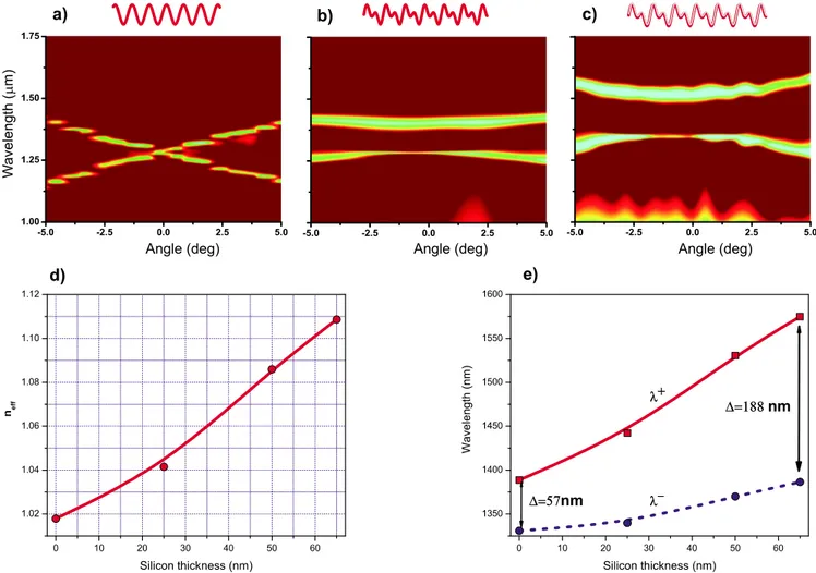
Figure2shows the wavelength dependent reflectivity map of different grating structures as a function of the incidence angle. The corresponding grating structures are schemati-cally shown on top of each dispersion curve. In Fig. 2共a兲, each band represents the forward and backward propagating SPPs on a uniform 共⌳1= 1 330 nm兲 grating structure. Uni-form grating compensates for the momentum mismatch and acts as a coupler. The second order diffraction from the uni-form grating is very weak; hence, SPPs on these types of periodic structures do not show a gap in the dispersion at the excitation wavelength. We note that the minigaps seen in the dispersion curve are due to the discreteness of measurements and the sharp resonances do not allow for interpolation. However, the addition of the second periodicity onto the first one results in a biharmonic structure and creates a back-scattering on the propagating SPPs and leads to the forma-tion of standing waves on the biharmonic grating structure. Since the SPPs localized on peaks and troughs of the peri-odic structure have different energies, a band gap opens up between these lower and higher energy bands, which is de-noted by+共or−兲 and −共or+兲, respectively. As seen in Fig. 2共b兲, the biharmonic structure 共⌳1= 1 330 nm+⌳2 = 665 nm兲 leads to a band gap with a width of ⌬=57 nm around the normal incidence. Controlling the properties of the surface of this structure is critical for fine tuning the characteristics of the band gap. We observe that depositing a thin layer of silicon with full coverage significantly changes the effective indices of the SPPs without perturbing the SPP excitation.
It is well known that the field distributions of + and− branches of SPPs at the band edges show different confine-ment behavior.25 Figure 3 shows the finite difference time domain 共FDTD兲 simulation results for the electric field
dis-FIG. 1. 共Color online兲 共a兲 Two-dimensional AFM image of biharmonic metallic surface. First, the periodicity is designed to couple free space light to SPPs. The second one generates the backscattering for propagating SPPs and opens up a photonic band gap.共b兲 Line profile of the AFM image.共c兲 Schematics of the double exposure method for grating fabrication. 共d兲 The surface plasmon dispersion curves on a flat metal surface and on uniform grating. A band gap opens up in the case of grating. Dispersion curve lies outside the light line.共e兲 The surface plasmon dispersion curves on a biharmonic grating. Dispersion with a larger grating component shows the band gap within the light line.
tributions on a biharmonic metallic grating structure illumi-nated with the wavelength of − and +, respectively. − localizes on the troughs while + localizes on the peaks of the periodic structure. It is seen that+and−show different confinement behavior. The field of + 关Fig. 3共b兲兴 becomes more confined to the interface than that of − 关Fig. 3共a兲兴. This extra confinement makes + more sensitive to the sur-face properties. Thus, loading the biharmonic metallic struc-ture with high dielectric material should increase the energy difference between the + and − bands, which would di-rectly affect the width of the band gap. This reasoning has been tested with the incremental loading of a metallic bihar-monic grating structure with silicon 共Si兲. Figure2共c兲shows the dispersion diagram of a biharmonic structure uniformly coated with a 50-nm-thick Si. The Si coating increases the central wavelength and widens the band gap. We systemati-cally changed the Si thickness and measured the dispersion. Figure2共d兲summarizes these results. There is an increase in effective indices of SPPs as the silicon thickness increases. From Eq.共1兲 for normal incidence illumination, the effective index of SPPs can be written as neff=/⌳. Figure2共d兲shows the measured effective indices neff of SPPs. The effective index can be tuned from neff= 1.02 to neff= 1.11. Finally, as seen from Fig.2共e兲, the deposition of a Si layer increases the
width of the band gap up to ⌬=188 nm. Thus, we demon-strate the ability to systematically control not only the effec-tive index but also the width of the band gap.
On grating structures, forward and backward propagating SPPs having a wavelength in the band gap destructively in-terfere. However, local perturbation of the effective index can lead to an extra phase change in the propagating waves and can result in a constructive interference at a specific wavelength, which is a cavity mode. Hence, the capability to control the local effective index of SPPs enables the fabrica-tion of plasmonic cavities on grating structures. Therefore, in
FIG. 2. 共Color online兲 Experimental dispersion curves of SPPs on 共a兲 uniform, 共b兲 biharmonic, 共c兲 silicon-loaded biharmonic metallic surface, and 共d兲 effective refractive indices as a function of silicon thickness. 共e兲 Wavelengths of upper and lower bands + and − as functions of silicon thickness.
FIG. 3. 共Color online兲 FDTD simulation results for the electric field distributions localized on the biharmonic metallic structure illuminated with wavelengths of− and +.
the presence of a cavity, SPPs with a previously forbidden wavelength can propagate when the following resonance condition is met:17,28
L ·⌬n = 共2m + 1兲
4, 共2兲
where L is the cavity length, ⌬n is the index perturbation, and is the central wavelength of the band gap. Therefore, we expect to observe a cavity mode at the central wave-length.
A mask with a number of cavities with the same geometry separated by 100 m to prevent a coupling between cavities on both sides in an area of 10⫻10 mm2, was used to litho-graphically define the cavity structure on the biharmonic metal surface, and a 65-nm-thick Si was deposited on surface outside the cavity regions. This approach is much simpler than the physical removal of periodicity in a grating. Further-more, this approach makes use of holographic lithography possible for cavity fabrication, eliminating the need for ex-tensive e-beam writing. Figure4共a兲is a schematic represen-tation of the cavity geometry. From Fig. 2共d兲, the effective refractive indices of SPPs in silicon-coated and uncoated re-gions are n0= 1.017 and n1= 1.108, respectively. The corre-sponding effective index difference is⌬n=0.091 and the re-sulting cavity length for the central wavelength of = 1.479 m is L = 4.1 m.
We performed FDTD simulations to verify the cavity for-mation. Figure4共b兲shows the simulation result of the elec-tric field intensity 共兩E2兩兲. It is seen that propagating SPPs form a standing wave inside the cavity region. This localiza-tion strongly depends on cavity size. According to the results of the simulation, the optimum cavity length was found be around 5.5 m, which is slightly larger than that obtained from Eq.共2兲, which is 4.1 m. The difference between the experiment and the simulation results from the small differ-ence between the refractive index of the evaporated Si and that assumed for the simulation. To clarify the cavity behav-ior, we measured the dispersion diagram. Figure5共a兲 repre-sents the dispersion diagram of the biharmonic grating struc-ture without the cavity and Fig. 5共b兲 shows the same structure with the cavity. An additional absorption peak
ap-pears in the band gap region. Red colored band represents the localized cavity mode. To increase the contrast in the dispersion diagram, the color scale was normalized to R = 80% and the diffraction background was subtracted from the reflection spectrum. This state shows a nondispersive property. The center of the absorption does not change as a function of the incidence angle, as would be expected from a localized state.11Figures 5共c兲and5共d兲show the normal in-cidence wavelength dependent reflectivity. In Fig. 5共c兲, two clear absorption peaks correspond to −and+at the band edges. The red arrow in Fig. 5共d兲 shows additional absorp-tion peak corresponding to the cavity mode. The decrement in the reflected intensity below the 1.3 m is due to the diffraction from the grating structure. Experimentally, we ob-serve the cavity state for a 4.5 m cavity length. The quality factor of the cavity, defined as Q =共⌬0/0兲, can be calcu-lated from the reflectivity spectrum. From Fig. 5共d兲, full width at half maximum of the cavity mode is approximately ⌬0⬇40 nm and the corresponding quality factor is Q=37. This quality factor is relatively low for plasmonic cavities as compared to photonic crystal cavities. The overall quality factor can be described as19
1 Q= 1 Qabs + 1 Qrad , 共3兲
where Qabsand Qrad are the radiative and absorptive quality factors, respectively. Qabsis dominated by the metallic loss in the plasmonic cavities and Qradby the out-of-plane radiative losses. Gratings that have a larger period component in the cavity region of the biharmonic grating can lead to signifi-cant radiative losses. The improvement in quality factor can be achieved by removing the grating structure inside the cav-ity region. Furthermore, the abrupt change in the localized mode profile in the cavity region is the other radiative loss source. Gently modifying the grating amplitude around the cavity may also suppress the radiation losses.29Gong et al.19 proposed the theoretical limit at low temperatures for the quality factor in the case of plasmonic cavities made using Bragg reflectors as 1000. However, experimental quality fac-tors measured on the cavities made of Bragg mirrors has been reported as 45.17
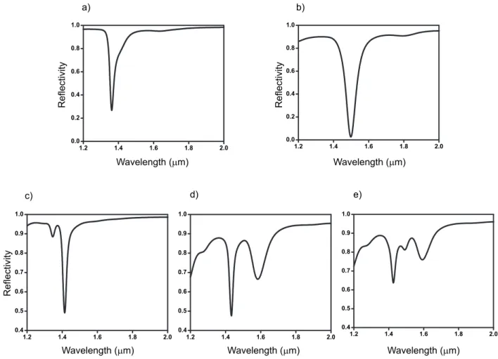
We have systematically studied the formation of plas-monic band gap cavities using numerical calculations. Shown in Fig. 6 are the FDTD simulation results of reflec-tivity on different grating structures. Figure 6共a兲 shows the normal incidence wavelength dependent reflectivity of a uni-form metallic grating having a periodicity of⌳1= 1330 nm. The clear absorption peak corresponds to the plasmonic reso-nance. Si loading onto the uniform metallic structure in-creases the effective refractive index of the propagating SPP. This increase in refractive index makes plasmonic resonance shift toward higher wavelengths. Figure 6共b兲 shows the shifted plasmonic resonance absorption on silicon-loaded uniform metallic grating structures. The second order diffrac-tion from the uniform metallic structure is weak and cannot create a band gap. As seen in Fig. 6共c兲 superimposing the second grating creates the band gap. Figure 6共c兲shows the reflectivity of biharmonic共⌳1= 1330 nm+⌳2= 665 nm兲 me-tallic grating structure. Two resonance peaks correspond to
FIG. 4. 共Color online兲 共a兲 Schematic of the plasmonic cavity structure.共b兲 FDTD simulation of the electric field distribution in a cavity illuminated with the cavity mode.
−and+, respectively. A narrow band gap becomes appar-ent when the second harmonic componappar-ent共⌳2= 665 nm兲 is superimposed on the grating structure. However, bare bihar-monic grating creates a narrow band gap and silicon loading can widen the width of the plasmonic band gap while in-creasing the effective refractive index. Figure6共d兲shows the reflectivity of the biharmonic共⌳1= 1330 nm+⌳2= 665 nm兲 metallic grating structure uniformly loaded with 50-nm-thick Si. Finally, Fig. 6共e兲 illustrates the reflectivity of the plas-monic cavity fabricated on silicon-loaded biharplas-monic metal-lic grating structure. Additional absorption inside the band gap corresponds to cavity resonance.
Many applications such as displays and light emitting de-vices require the use of the visible part of the spectrum. It would therefore be important to demonstrate that the physi-cal principles and fabrication technology is suitable for the plasmonic cavity formation in the visible, as well. Thus, a plasmonic band gap cavity in the visible regime was de-signed and fabricated. In this case, the biharmonic structures consisted of gratings with periods of ⌳1= 500 nm and ⌳2 = 250 nm used for coupling and band gap formation, respec-tively. A spectroscopic ellipsometer共WVASE32兲 was used to measure the reflection in the visible wavelength range. The normal incidence reflectivity of biharmonic structures 关Fig. 7共a兲兴 reveals a wide band gap region in the absence of a silicon layer. To fabricate the cavity, a 12-nm-thick Si
load-ing was used for the particular cavity geometry and a 4.5 m cavity length was defined. A plasmonic cavity was obtained in the visible regime; a cavity state appears inside the band gap as expected关Fig.7共b兲兴. The effect of the ultra-thin layer of Si on the transmission of light is negligible. The effective refractive index of the SPPs strongly depends on the thickness of the Si loading and restricts systematic stud-ies at visible wavelengths. Uncertainty in our silicon deposi-tion rates makes it difficult to control and the effective indi-ces at the level of the precision are required for a more systematic study. Other materials with high dielectric con-stants may also be used for the same purpose.
III. CONCLUSION
In conclusion, we have used a grating to couple light to the surface plasmons and a second grating superposed onto the first to create a band gap at the excitation wavelength of the first grating. We demonstrated that two superposed grat-ing structures result in a band gap covergrat-ing the excitation wavelength region. We showed that the band gap widths of grating based plasmonic structures can be controlled with the deposition of high dielectric layers. By selective deposition, we have demonstrated the formation of plasmonic cavities
FIG. 5. 共Color online兲 Experimental dispersion curves of SPPs on a biharmonic structure 共a兲 without a cavity, 共b兲 with a cavity, and 关共c兲 and共d兲兴 normal incidence reflectivity spectrum for 共a兲 and 共b兲, respectively.
through the use of biharmonic grating structures with high dielectric superstructures. We observe cavity modes both in the infrared and the visible part of the spectrum. The ap-proach we use is simple, combining holographic lithography
with photolithography to fabricate plasmonic band gap cavi-ties. This approach is suitable for large area applications and it makes plasmonic cavities applicable in examining cavity material interactions.
FIG. 6. FDTM simulation results for the reflectivity of different grating structures.共a兲 Uniform grating 共⌳1= 1330 nm兲. 共b兲 50 nm Si loaded uniform grating 共⌳1= 1330 nm兲. 共c兲 Biharmonic metallic grating 共⌳1= 1330 nm+⌳2= 665 nm兲. 共d兲 Biharmonic 共⌳1= 1330 nm+⌳2= 665 nm兲 metallic grating structure uniformly loaded with a 50-nm-thick Si. 共e兲 Plasmonic cavity fabricated on silicon-loaded biharmonic metallic grating structure.
FIG. 7. Normal incidence reflectivity spectrum of共a兲 the biharmonic and 共b兲 the biharmonic with cavity structure in a visible wavelength range. A cavity state appears inside the band gap region.
ACKNOWLEDGMENTS
The authors gratefully acknowledge the financial support of the Turkish Scientific and Technical Research Council
共TUBITAK兲, Grant No. 104M421, UNAM for the use of the FTIR spectrometer and AFM, A. Dana for his help in AFM measurement and graphics software, and O. F. Ilday for the critical reading of the manuscript.
*Author to whom correspondence should be addressed; [email protected]
1H. Raether, Surface Plasmons共Springer–Verlag, Berlin, 1986兲. 2W. L. Barnes, A. Dereux, and T. W. Ebbesen, Nature 共London兲
424, 824共2003兲.
3J. Homola, S. S. Yee, and G. Gauglitz, Sens. Actuators B 54, 3 共1999兲.
4J. S. Biteen, L. A. Sweatlock, H. Mertens, N. S. Lewis, A. Pol-man, and H. A. Atwater, J. Phys. Chem. C 111, 13372共2007兲. 5M. Derouard, J. Hazart, G. Lerondel, R. Bachelot, P. M. Adam,
and P. Royer, Opt. Express 15, 4238共2007兲.
6S. I. Bozhevolnyi and V. S. Volkov, Opt. Lett. 26, 734共2001兲. 7H. J. Lezec, J. A. Dionne, and H. A. Atwater, Science 316, 430
共2007兲.
8W. L. Barnes, J. Opt. A, Pure Appl. Opt. 8, S87共2006兲. 9T. A. Kelf, Y. Sugawara, R. M. Cole, J. J. Baumberg, M. E.
Abdelsalam, S. Cintra, S. Mahajan, A. E. Russell, and P. N. Bartlett, Phys. Rev. B 74, 245415共2006兲.
10U. Kreibig and M. Vollmer, Optical Properties Metal Clusters 共Springer, Berlin, 1995兲.
11N. M. B. Perney, F. J. G. de Abajo, J. J. Baumberg, A. Tang, M. C. Netti, M. D. B. Charlton, and M. E. Zoorob, Phys. Rev. B 76, 035426共2007兲.
12A. V. Zayats and I. I. Smolyaninov, J. Opt. A, Pure Appl. Opt. 5, S16共2003兲.
13M. Moskovits, Rev. Mod. Phys. 57, 783共1985兲.
14K. Kneipp, Y. Wang, H. Kneipp, L. T. Perelman, I. Itzkan, R. Dasari, and M. S. Feld, Phys. Rev. Lett. 78, 1667共1997兲. 15S. M. Nie and S. R. Emery, Science 275, 1102共1997兲. 16J. A. Sánchez-Gil, Opt. Lett. 32, 2330共2007兲.
17J. C. Weeber, A. Bouhelier, G. C. des Francs, L. Markey, and A. Dereux, Nano Lett. 7, 1352共2007兲.
18B. Wang and G. P. Wang, Appl. Phys. Lett. 87, 013107共2005兲. 19Y. Y. Gong and J. Vulkovic, Appl. Phys. Lett. 90, 033113
共2007兲.
20J. D. Joannopoulos, R. D. Meade, and J. N. Winn, Photonic
Crystals共Princeton University Press, New Jersey, 1995兲.
21J. A. S. Gil, Opt. Express 32, 2330共2007兲.
22Z. W. Liu, Q. H. Wei, and X. Zhang, Nano Lett. 5, 957共2005兲. 23R. H. Ritchie, E. T. Arakawa, J. J. Cowan, and R. N. Hamm,
Phys. Rev. Lett. 21, 1530共1968兲.
24S. C. Kitson, W. L. Barnes, and J. R. Sambles, Phys. Rev. Lett.
77, 2670共1996兲.
25W. L. Barnes, T. W. Preist, S. C. Kitson, and J. R. Sambles, Phys. Rev. B 54, 6227共1996兲.
26A. C. R. Pipino, R. P. VanDuyne, and G. C. Schatz, Phys. Rev. B
53, 4162共1996兲.
27A. Kocabas and A. Aydinli, Opt. Express 14, 10228共2006兲. 28R. C. Alferness, C. H. Joyner, M. D. Divino, M. J. R. Martyak,
and L. L. Buhl, Appl. Phys. Lett. 49, 125共1986兲.
29Y. Akahane, T. Asano, B. S. Song, and S. Noda, Nature共London兲