Structural and Corresponding Magnetic Properties
of Sputtered Ni/Al Multilayer Films:
Effect of Ni Layer Thickness
A. Karpuz
a,∗, H. Köçkar
band S. Çölmekç
.
IbaDepartment of Physics, Kamil Ozdag Science Faculty, Karamanoglu Mehmetbey University, Karaman, Turkey bDepartment of Physics, Science and Literat. Faculty, Balikesir University, Balikesir, Turkey
(Received April 25, 2018; revised version July 24, 2018; in final form August 21, 2018)
A series of Ni/Al multilayers with different thicknesses of Ni layers was produced by a sputtering technique. The deposition parameters of optimum magnetic properties for write heads were detected by scanning the magnetic layer thickness from 0 to 70 nm. The optimum magnetic properties were decided by obtaining the saturation magnetization, Ms, coercivity, Hcand Ms/Hcratios from the hysteresis loops. A face centered cubic (fcc) structure was established for all films. Transition surface morphology; i.e., a surface morphology between an apical + uneven structure (observed for the mono layered Al film) and an acicular + relatively smooth structure (observed for the films with Ni layer thicknesses of 30 nm and 70 nm) occurred on the surface of the film with Ni layer thickness of 10 nm. This transition surface morphology was very similar to that of the substrate as compared to the other morphologies and it may lead to relatively lower Hcvalue. A significant increase in Hcvalue was detected for Ni/Al film with Ni layer thickness of 70 nm. The increase was attributed to the irregular acicular morphology of substrate and high crystallite size of Al fcc (111). The deposition parameters of 8[Ni(10 nm)/Al(10 nm)] multilayer can be considered in order to support the higher Ms/Hcratio which has a key role for effective technological applications of write heads.
DOI:10.12693/APhysPolA.134.1180
PACS/topics: layer thickness, magnetic properties, Ni/Al multilayers, sputtering system
1. Introduction
Several types of magnetic materials, includ-ing alloys [1], multilayer films [2] and multilayer nanowires [3, 4], have been used in a lot of studies in recent years. There are a lot of advantages in focusing on magnetic thin films since their applications are rapidly expanding in technology [5]. Ni/Al is a very useful magnetic multilayer and it has also been used by various researchers in several studies. For example, Kuk et al. [6] recently studied the effect of Al/Ni atomic ratio on Al/Ni multilayers and Noro et al. [7] investigated the intermetallic phase formation in Ni/Al multilayers. Besides, Simões et al. [8] focused on the anisothermal solid-state reactions for Ni/Al multilayer thin films while Tixier et al. [9] were interested in the relation of indentation hardness measurements of Ni3Al/Ni
multilayers with the structural properties of the layers. In addition, Kang et al. [10] reported the phenomenon of magnetic anisotropy for Ni/A1 multilayers prepared by a sputtering technique. However, the limited number of studies on magnetic hysteresis loop properties of sputtered Ni/Al multilayers is obvious in literature.
The magnetic properties of a film take over an im-portant position in data storage and in the relevant ar-eas [11]. In general, saturation magnetization, Ms,
re-manent magnetization and coercivity, Hc are the main
∗corresponding author; e-mail: [email protected]
magnetic properties which disclose the characteristics of a magnetic material [12, 13]. The soft magnetic materials which have the low Hcvalues are the unique components
for the important devices, for example, motors, relays and transformers [14]. In addition, the high Ms values
are necessary to reduce their dimensions and obtain ef-fective small devices [15]. The magnetic materials with high Ms and low Hc are very promising for the
mag-netic technology [16], especially for write heads [17, 18]. This magnetic condition is also valid for devices which contain a typical electromagnet [14]. These magnetic properties can be easily adjusted according to intended scope since they are mainly affected by various effects in a film such as a change in crystalline structure [19, 20]. The crystalline structure can be considerably changed by changing production parameters during the film de-position. The sputtering technique is one of the many deposition techniques which have adjustable production parameters affecting the structural properties of a film. It is often used to produce thin or ultra thin films of high quality [21].
In this study, the effect of different thicknesses of mag-netic layers on the structural and magmag-netic hysteresis loop properties of Ni/Al multilayer films was studied and the deposition parameters of optimum magnetic proper-ties for write head materials in a hard disk drive were determined by investigating Ms/Hcratios obtained from
the magnetic hysteresis loops of the films. Besides, de-spite the limited number of studies on properties of sput-tered Ni/Al multilayers, this study compares the ob-tained results with those of literature.
2. Experimental details
A series of Ni/Al multilayer films was produced by a sputtering technique from high purity commercial Ni and Al targets located onto the DC magnetrons. The deposi-tion was achieved on the commercial acetate substrates (4.5 cm×2.5 cm) at room temperature (around 25◦C). The substrate temperature varied by ±5◦C because of the sputtering process during the film production. The substrate was far from the targets by about 12.5 cm. The lowest pressure value of the chamber was 5 × 10⁻⁵ mbar and it increased to around 5×10⁻³mbar during the sput-tering process due to sending of argon into the chamber. The thickness measurements of each layer were based on a quartz crystal microbalance thickness monitor. Total film thickness and the thickness of each Al layer were ad-justed as 160 nm and 10 nm, respectively. On the other hand, the thickness of Ni layers was changed gradually as 0, 10, 30, and 70 nm to investigate the effect of dif-ferent thicknesses of Ni layers on the properties of multi-layers. For better understanding, schematic illustrations of the sputtered multilayers of 8[Ni(10 nm)/Al(10 nm)] and 4[Ni(30 nm)/Al(10 nm)] are given in Fig. 1a and b, respectively. The deposition rates of Ni and Al were
Fig. 1. Schematic illustrations of the sputtered multi-layers: (a) 8[Ni(10 nm)/Al(10 nm)], (b) 4[Ni(30 nm) /Al(10 nm)].
kept constant as 0.05 nm/s for all productions. For all multilayers, a Ni layer was firstly sputtered onto the sub-strate and then, an Al layer (10 nm) was deposited onto this Ni layer. This procedure was repeated until obtain-ing the total film thickness (160 nm). The compositional analysis was done using an energy dispersive X-ray spec-troscopy (EDX, BRUKER) during the surface monitor-ing carried out by a scannmonitor-ing electron microscope (SEM, ZEISS EVO LS 10). The crystal structure analysis was performed by using an X-ray diffractometer (BRUKER) with the X-ray diffraction (XRD) technique. The Bragg angle was scanned between 30◦and 100◦ and the Cu Kα
radiation was used to obtain the XRD patterns of the multilayers. In addition, the surface monitoring was im-proved with the images of the atomic force microscope (AFM, NanoMagnetics Instruments). Hysteresis loops of the multilayers were obtained with a vibrating sam-ple magnetometer (VSM, ADE TECHNOLOGIES DMS-EV9) by sending the magnetic field parallel to the film plane. The measurements were achieved at room temper-ature by creating the magnetic field intensity of 20 kOe and scanning its intensity between ±20 kOe. The Ms
values were detected by considering the complete volume of each film.
3. Results and discussion
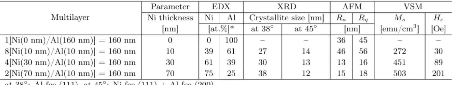
The data from elemental analysis show that the films that have Ni layer thickness of 0, 10, 30, and 70 nm contain 0%, 39%, 61%, and 75% Ni atoms, respectively, as shown in Table I. According to the results, the Ni content in the films gradually increased with the in-creasing thickness of Ni layers. Also, it was detected that the rest of the films include only Al atoms. Al-though the films have a multilayered structure, the in-dicated atomic contents are total quantities of Ni or Al atoms in the investigated Ni/Al films. The crys-talline structure analysis done by XRD shows that the all films are in the face centered cubic (fcc) form. The XRD patterns of the films are shown in Fig. 2. Some differences were observed in the peaks of the diffrac-tion patterns with the change of magnetic layers thick-ness. Namely, the intensity of Al fcc (111) peak which occurred at around 38◦ Bragg angle decreased gradu-ally as the thickness of Ni layers increased (see Fig. 2).
TABLE I Analysis data of Ni/Al multilayers sputtered by considering different thicknesses of Ni layers
Multilayer
Parameter EDX XRD AFM VSM
Ni thickness Ni Al Crystallite size [nm] Ra Rq Ms Hc
[nm] [at.%]* at 38◦ at 45◦ [nm] [emu/cm3] [Oe]
1[Ni(0 nm)/Al(160 nm)] = 160 nm 0 0 100 – – 36 45 – –
8[Ni(10 nm)/Al(10 nm)] = 160 nm 10 39 61 27 14 46 56 272 30
4[Ni(30 nm)/Al(10 nm)] = 160 nm 30 61 39 30 13 13 16 451 89
2[Ni(70 nm)/Al(10 nm)] = 160 nm 70 75 25 38 12 15 18 503 201
at 38◦: Al fcc (111), at 45◦: Ni fcc (111) + Al fcc (200)
Fig. 2. XRD patterns of Ni/Al multilayers deposited by considering different thicknesses of Ni layers.
The XRD pattern of multilayer with 10 nm Ni thickness has the highest peak intensity of fcc (111) plane of Al among the Ni/Al multilayers. Also, the intensities of the (220) and (311) peaks decreased with the increase of Ni layer thickness and hence Ni content in the films and they disappeared from the patterns of the films with 30 nm and 70 nm Ni layer thickness. Beside these peaks, there is one more peak located at around 45◦Bragg angle and its intensity increases with the increase of Ni content. Since this peak already exists at the XRD pattern of the pure Al film and its intensity increases with the increasing Ni content, it was assumed as Ni fcc (111) + Al fcc (200). In other words, this peak was labelled as a mixture of (111) and (200) planes of fcc structure for Ni and Al, respec-tively. The peaks observed at around 38◦and 45◦ in the XRD patterns of the Ni/Al multilayers investigated in the present study were also observed in the XRD pattern of the as-deposited 5[Ni(200 Å)/(Al(100 Å)] multilayer investigated in [22] as Al (111) and Ni(111)/Al(200), respectively. The main peak was the latter. On the other hand, Ni (222) reflection observed at around 98◦ Bragg angle in the XRD pattern of the multilayer in study [22] was not observed in this study. Besides, the peaks observed at around 38◦and 45◦were also detected in the XRD pattern of the as-deposited Al-rich multi-layer, 5[Ni(50 Å)/(Al(227 Å)], investigated in study [22]. For Al-rich multilayer in [22], the main peak was Al (111) as observed for the 8[Ni(10 nm)/Al(10 nm)] multilayer in-vestigated in this study. This can be attributed to Al-rich content of the multilayers (see Table I). In a study [23] aimed to investigate the XRD results in situ heating of
large period Ni/Al multilayer, a strong peak was detected at ≈ 44◦ Bragg angle of XRD pattern of “as-deposited” Ni/Al multilayers corresponding to the (111) plane for solid solution of Ni(Al). For XRD results, some differ-ences were reported between a study [10] done by Kang et al. and the present study. It was found in study [10] that Ni(25 Å)/Al(35 Å) multilayer has only Ni (111) peak at around 44◦ angle. On the other hand, the characteristic (200) peak of the fcc structure that occurred at around 51◦ Bragg angle was marked as a plane of Ni according to JCPDS card for Ni numbered as 04-0850. The diffrac-tion pattern of the substrates was also given in Fig. 2 and it was understood that any crystalline formation was not obtained, unlike those of the films investigated. The crys-tallite size of each observed plane in the XRD patterns of multilayer structure was also calculated by the Scherrer equation, as given in [24]. The crystallite sizes were cal-culated for two considerable peaks in the XRD patterns of the multilayer systems. It was found that the sizes of Al fcc (111) crystallites are 27, 30, and 38 nm, and the sizes of Ni fcc (111) + Al fcc (200) crystallites are 14, 13, and 12 nm for the multilayers with 10, 30, and 70 nm Ni layer thicknesses, respectively. The values are also listed in Table I. The crystallite size of Ni fcc (111) + Al fcc (200) slightly decreased, whereas that of Al fcc (111) crystallite increased as the Ni layers thickness increased. In addition, it can be assumed that (111) preferential tex-ture of the pure Al film exists for the Ni/Al multilayers sputtered with different thicknesses of Ni layers because the intensity of Ni fcc (111) component of overlapped peaks detected at around 45◦ Bragg angle is expected to increase as the thickness of Ni layers increases. Fur-thermore, the XRD pattern given in [25] for as-deposited Ni–25 at.% Al at room temperature shows some similar-ities to that of the Ni/Al multilayer has Ni layer thick-ness of 70 nm (75 at.% Ni/25 at.% Al) investigated in this study, especially concerning the overlapped peaks formed at around 45◦. However, there is no any peak formation at around 51◦ Bragg angle in the XRD pattern shown in [25] for as-deposited Ni–25 at.% Al at room temper-ature, unlike the present study. This may arise from multilayered structure of the investigated films.
Figure 3 shows the SEM images of the films pro-duced with different thicknesses of Ni layers. It is ob-viously shown from Fig. 3a that the surface of the pure Al film produced as a mono layered structure, unlike the other films, is covered with a lot of grains having around 200 nm diameters. These grains disperse almost homogeneously onto the film surface. The other parts of Fig. 3 illustrate the SEM images of the multilayer films investigated according to different thicknesses of magnetic layers. It was shown that these surface mor-phologies are in almost similar form. In other words, the surface morphology observed with SEM is indepen-dent of change in the thickness of Ni layers. In addi-tion, few clustered regions on the surface of the film with Ni layer thickness of 30 nm did not change this gen-eral situation of the surface morphology (see Fig. 3c).
Fig. 3. SEM images of the films produced considering different thicknesses of Ni layers: (a) 0 nm (pure Al film), (b) 10 nm, (c) 30 nm, (d) 70 nm.
This may be attributed to some inconsiderable experi-mental errors arising from different deposition processes. The surface of Ni/Al film (1 nm Ni and 6 nm Al), as-deposited and after heating to 800◦C, was also exam-ined by using SEM in study [26] reporting the effect of the Ni/Al bilayer film thickness on the density of the single-walled carbon nanotubes. It was expressed that the surface morphology of the as-deposited multi-layer was generally featureless. However, some clusters were formed on the surface of the heated Ni/Al mul-tilayer. It can be deduced that the surface morphol-ogy of the heated Ni/Al multilayer in [26] is more sim-ilar to those of the present study than the as deposited one, although an oxidized Si substrate was used, unlike the present study.
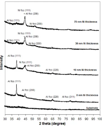
AFM images of the films were investigated and given in Fig. 4 together with that of the substrate used. AFM im-age observed for mono layered Al film is shown in Fig. 4a. This surface has a great number of separate apical and uneven regions. The regions can be clearly distinguished because of their relatively light colors which indicate rel-atively high points in the AFM images. Therefore, the surface of this film can be described as a relatively rough surface. The surface morphology started to change when the Ni layer thickness was adjusted as 10 nm. The sur-face became moderate about separate regions, whereas the rough surface existed (see Fig. 4b) for the composi-tions of 39 at.% Ni and 61 at.% Al. This type of surface can be assumed as a transition formation from an api-cal and uneven structure to an acicular morphology as seen in Fig. 4c and d. On the other hand, this transi-tion morphology has a considerable region with relatively
high altitude and the size of this region is about 2 µm (see Fig. 4b). This formation can be attributed to the irregular structure which was called as transition mor-phology. An acicular surface morphology was observed for the Ni/Al multilayers which have Ni layers thick-nesses of 30 nm and 70 nm, as shown from Fig. 4c and d. The observed acicular morphologies are of vertical type in this study. Similar acicular morphologies were also observed on the surface of as-deposited Ni/Al multilay-ers examined in study [22] although they have different thickness value from those of the multilayers investigated in this study. Roughness parameters, Ra and Rq (root
mean square), were also calculated during the AFM ob-servation. Ra values are 36, 46, 13, and 15 nm, while
Rq values are 45, 56, 16, and 18 nm for the surfaces
of the films with Ni layer thickness of 0, 10, 30, and 70 nm, respectively. It was understood that the con-siderable region with relatively high altitude observed on the surface of multilayer with Ni layer thickness of 10 nm caused an increase in Ra and Rq values. In addition, the
acicular morphologies observed on the surfaces of films with 30 nm and 70 nm Ni layers thicknesses have rela-tively a smooth structure according to roughness param-eters. However, the acicular morphology observed on the surface of the film with Ni layer thickness of 30 nm is more homogeneous than that of the film with Ni layer thickness of 70 nm. This can be clearly seen from lo-cal regions with different altitudes in AFM images of the film with Ni layers thickness of 70 nm. In other words, some considerable regions of acicular morphology on the surface of the film with Ni layer thickness of 70 nm have higher altitude than the rest regions (see Fig. 4d).
Fig. 4. AFM images of the Ni/Al multilayers having different thicknesses of Ni layers: (a) 0 nm (pure Al film), (b) 10 nm, (c) 30 nm, (d) 70 nm and AFM image for the substrate which was used for deposition.
It was concluded that the surface morphology trans-formed from a structure with apical and uneven clumps to an acicular and relatively smooth morphology when the thickness of Ni layers was gradually increased from 0 nm to 70 nm. Also, magnetic layer thickness has a significant role on the film surface and acicular morphol-ogy becomes highly irregular when the thickness of Ni layers increases from 30 nm to 70 nm. A different type of irregularity in the acicular morphology was also seen in study [22]. A more homogeneous and regular acicular surface morphology was detected for as-deposited Al-rich multilayer than that of the other as-deposited multilayer examined in [22]. Besides, the surface of the substrate was also examined by AFM for better investigation of the film surfaces and its image was also given in Fig. 4. It is clearly shown from its color scale that the substrate surface is clear and smooth in comparison with those of the investigated films. It can be also emphasized that the surface morphology of 8[Ni(10 nm)/Al(10 nm)] mul-tilayer is the most similar to that of the substrate.
Magnetic behavior was revealed by measuring Msand
Hcvalues for all Ni/Al multilayers. The hysteresis curves
of the films were plotted in Fig. 5. As shown from the figure, pure Al film does not have any hysteresis and this is an expected situation since it is a non-magnetic
ma-terial. On the other hand, the Msvalues were 272, 451,
and 503 emu/cm3 for the films with Ni layer thicknesses
of 10, 30, 70 nm, respectively. The values are propor-tional to the atomic Ni contents in the films. Ms value
increases with increasing Ni content as shown in Table I. This is also an expected situation since the magnetization is depending mainly on the contents of Ni atoms for in-vestigated Ni/Al multilayers. Hcvalues were found as 30,
89, and 201 Oe for the films with Ni layer thicknesses of 10, 30, 70 nm, respectively as shown in Table I. The Hc
value also increases with increase of Ni layer thickness and hence Ni content of the films. This is an anoma-lous situation regarding the relation between coercivity and non-magnetic content. It is stressed in [14] that an increase in non-magnetic content results in an increase in coercivity, unlike the present study. It can be un-derstood that the change in Hc values is also related to
the change in the structural properties. The lowest Hc
value was obtained for the film with Ni layer thickness of 10 nm (for the highest Al content, 61 at.% Al) (see Ta-ble I). This is most probably related to the surface sim-ilarity of the substrate and this multilayer (see Fig. 4). Namely, a growth which is compatible with the substrate surface may support the low coercivity. In addition, a vertical acicular morphology may lead to increase of Hc
Fig. 5. Hysteresis loops of the Ni/Al multilayers hav-ing different thicknesses of Ni layers.
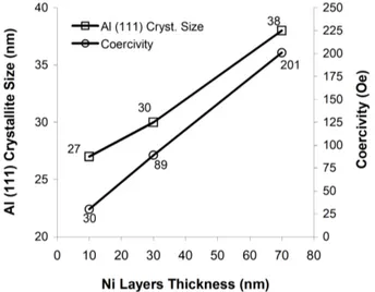
Fig. 6. Size of Al (111) crystallite and Hc values de-pending on the thickness of Ni layers.
Fig. 7. Ms and Hcvalues depending on Ni contents of the Ni/Al multilayers.
values. As stated in study [16] which investigated the hollow fibers with high Msand while comparatively low
Hc, the Hc is mainly affected by the surface
morphol-ogy. It was concluded in the present study that the ir-regular structure of acicular morphology and relatively high size of Al fcc (111) crystallite enhance the increase in Hc values as found in Ni/Al multilayer with Ni
lay-ers thickness of 70 nm. As clearly seen in Fig. 6, the change in the size of Al fcc (111) crystallite is compatible with the change in Hc values when the thickness of Ni
layers increases. Besides, it was calculated that Ms/Hc
value gradually decreased when the thickness of Ni lay-ers increased. The multilayer with Ni layer thickness of 10 nm has the highest Ms/Hc ratio among the films
pro-duced as shown in Fig. 7. This causes relatively less hysteresis losses together with relatively high saturation flux density in the materials in comparison with the oth-ers. Hence, it leads to more effective magnetic materials for technological write head applications [14, 15].
4. Conclusions
Ni/Al multilayers were studied to detect the deposition parameters of optimum magnetic properties for their po-tential use as write head materials in a hard disk drive. The films were obtained by considering different thick-nesses of magnetic layers with the sputtering technique. For all films, atomic Ni contents are compatible with the increasing thickness of Ni layers. The fcc structure was detected for all multilayers. The surface changed from an uneven and rough structure to an acicular and relatively smooth morphology for increasing Ni layer thickness from 0 nm to 70 nm. A transition morphology between these morphologies was observed for the Ni layer thickness of 10 nm and this morphology was similar to that of the substrate, unlike the other morphologies. Msvalues were
proportional to the atomic Ni content and Msand Hc
val-ues increased with the increase of Ni layer thickness. It was found that a film surface which is similar to substrate surface may be responsible for low Hc values, whereas
an irregular acicular morphology and high size of Al fcc (111) crystallite may cause an increase in Hc values. The
lowest Hc value and the highest Ms/Hc ratio were
ob-tained for the film with Ni layer thickness of 10 nm. Therefore, among the investigated multilayers, the opti-mum magnetic properties were obtained for the film with Ni layer thickness of 10 nm, i.e., 8[Ni(10 nm)/Al(10 nm)]. It is concluded that the deposition parameters of this film can be considered to obtain more effective materials for technological write head applications.
Acknowledgments
This study was financially supported by the Kara-manoğlu Mehmetbey University under Grant no 17-M-15, and by the State Planning Organization/Turkey un-der Grant no. 2005K120170 for Sputtering and the VSM systems. The authors would like to thank Hilal Kuru and Mehmet Uçkun for their contributions during the
film production and measurements. The authors are also grateful to the Karamanoğlu Mehmetbey Univer-sity/Karaman for the AFM imaging and the XRD mea-surements, and Selçuk University/Konya for the EDX measurements and the SEM images.
References
[1] H. Kockar, M. Alper, T. Sahin, O. Karaagac, J. Magn. Magn. Mater. 322, 1095 (2010).
[2] Y.S. Yu, Hai-Bo Li, W.L. Li, Mei Liu, Yu-Mei Zhang, W.D. Fei,J. Magn. Magn. Mater. 322, 1770 (2010). [3] R.S. Liu, S.C. Chang, I. Baginskiy, S.F. Hu,
C.Y. Huang,Pramana J. Phys. 67, 85 (2006). [4] M. Chen, P.C. Searson, C.L. Chien, J. Appl. Phys.
93, 8253 (2003).
[5] P.C. Andricacos, N. Robertson, IBM J. Res. Devel-opm. 42, 671 (1998).
[6] S.W. Kuk, H.J. Ryu, J. Yu, J. Alloys Comp. 589, 455 (2014).
[7] J. Noro, A.S. Ramos, M.T. Vieira,Intermetallics 16, 1061 (2008).
[8] S. Simões, F. Viana, A.S. Ramos, M.T. Vieira, M.F. Vieira,Intermetallics 19, 350 (2011).
[9] S. Tixier, P. Böni, H. Van Swygenhoven,Thin Solid Films 342, 188 (1999).
[10] S.S. Kang, J.W. Feng, G.J. Jin, M. Lu, X.N. Xu, A. Hu, S.S. Jiang, H. Xia, J. Magn. Magn. Mater. 166, 277 (1997).
[11] G.R. Pattanaik, D.K. Pandya, S.C. Kashyap, Thin Solid Films 433, 247 (2003).
[12] H. Kockar, M. Alper, H. Kuru, T. Meydan, J. Magn. Magn. Mater. 304, e736 (2006).
[13] H. Kuru, M. Alper, H. Kockar, J. Optoelec-tron. Adv. Mater. Symp. 1, 432 (2009).
[14] D. Jiles, Introduction to Magnetism and Magnetic Materials, Chapman and Hall, London 1991.
[15] T. Osaka, M. Takai, K. Hayashi, K. Ohashi, M. Saito, K. Yamada,Nature 392, 796 (1998).
[16] G.-Fang Liu, Z.-Dong Zhang, F. Dang, C.-Bing Cheng, C.-Xin Hou, S.-Da Liu,J. Magn. Magn. Mater. 412, 55 (2016).
[17] N.X. Sun, S.X. Wang,IEEE Trans. Magn. 36, 2506 (2000).
[18] X. Liu, G. Zangari, in: Magnetic Materials, Processes, and Devices VI: Applications to Stor-age and Microelectromechanical Systems (MEMS): Proc. Int. Symp., Eds. S. Krongelb, L.T. Romankiw, J.W. Chang, W. Schwarzacher, C.H. Ahn, Electro-chemical Society, Pennington (NJ) 2001, p. 211. [19] I.Z. Rahman, M.V. Khaddem-Mousavi, A.A. Gandhi,
T.F. Lynch, M.A. Rahman,J. Phys. Conf. Series 61, 523 (2007).
[20] B.B. Straumal, A.A. Mazilkin, S.G. Protasova, S.V. Dobatkin, A.O. Rodin, B. Baretzky, D. Goll, G. Schütz,Mater. Sci. Eng. A 503, 185 (2009). [21] J.B. Yi, Y.Z. Zhou, J. Ding, G.M. Chow, Z.L. Dong,
T. White, XingYu Gao, A.T.S. Wee, X.J. Yu, J. Magn. Magn. Mater. 284, 303 (2004).
[22] M. Swain, S. Singh, S. Basu, D. Bhattacharya, R.B. Tokas, M. Gupta, J. Alloys Comp. 631, 46 (2015).
[23] Z. Świątek, A. Gradys, Ł. Maj, J. Morgiel, K.W. Marszałek, R. Mania, M. Szlezynger, Acta Phys. Pol. A 130, 880 (2016).
[24] R.A. Mahesh, R. Jayaganthan, S. Prakash, V. Chawla, R. Chandra, Mater. Chem. Phys. 114, 629 (2009).
[25] P.Y. Li, H.M. Lu, S.C. Tang, X.K. Meng,J. Alloys Comp. 478, 240 (2009).
[26] R.Y. Zhang, I. Amlani, J. Baker, J. Tresek, R.K. Tsui, Nano Lett. 3, 731 (2003).