COMMUNICATION
Cite this:Nanoscale, 2015, 7, 6481 Received 15th December 2014, Accepted 12th March 2015 DOI: 10.1039/c4nr07395a www.rsc.org/nanoscale
Observation of polarized gain from aligned
colloidal nanorods
†
Yuan Gao,
a,bVan Duong Ta,
bXin Zhao,
a,bYue Wang,
aRui Chen,
aEvren Mutlugun,
‡
a,bKah Ee Fong,
bSwee Tiam Tan,
bCuong Dang,
bXiao Wei Sun,
bHandong Sun*
a,band Hilmi Volkan Demir*
a,b,cIn recent years, colloidal semiconductor nanorods have attracted great interest for polarized spontaneous emission. However, their polarized gain has not been possible to achieve so far. In this work we show the highly polarized stimulated emission from the densely packed ensembles of core-seeded nanorods in a cylindri-cal cavity. Here CdSe/CdS dot-in-rods were coated and aligned on the inner wall of a capillary tube, providing optical feedback for the nanorod gain medium. Results show that the polarized gain originates intrinsically from the aligned nanorods and not from the cavity and that the optical anisotropy of the nanorod ensemble was amplified with the capillary tube, resulting in highly polarized whispering gallery mode lasing. The highly polarized emission and lasing, together with easy fabrication andflexible incorporation, make this microlaser a promising candidate for important color conversion and enrichment applications including liquid crystal display backlighting and laser lighting.
Semiconductor nanocrystals are attractive materials offering numerous applications ranging from bioimaging1 to
opto-electronic devices, including light emitting diodes (LEDs),2
solar cells,3and lasers.4,5Over the past thirty years, the
devel-opment of colloidal nanocrystals has led to the achievement of high photoluminescence (PL) quantum yields with narrow emission linewidths as well as tunability of the peak emission
wavelength from the ultraviolet to the infrared by tailoring the size, structure and/or chemical composition.6 In addition,
solution-based processing of these colloidal semiconductor nanoparticles has allowed for low-cost fabrication, essentially at any substrate, for diverse photonic devices.
Given the nanoscale size of semiconductor nanoparticles, their density of electronic states is atomic-like because of the quantum confinement effect, which makes the emission wave-length and optical gain of this class of material less sensitive to temperature.4Meanwhile, their better photostability as
com-pared to organic dyes, combined with their rare earth element free nature, makes nanocrystals promising candidates for potential applications in lasers.7
Lasing from semiconductor nanocrystals was first demon-strated in 1991 by optical pumping CdSe nanocrystal doped glass at 80 K.8 However, under strong excitation that creates
multiexcitons, Auger recombination becomes an undesired non-radiative channel, a competing process for stimulated emission.9–11 In order to suppress the Auger recombination, the concept of single exciton gain was introduced and realized using type-II nanocrystals where electrons and holes are dis-tributed separately in cores and shells of the semiconductor nanocrystals.12However, adopting type-II nanocrystals leads to
an extreme reduction in the overlap of electron and hole wave-functions so that the emission transition rate is decreased sig-nificantly. In addition, recent type-I nanocrystal lasers operat-ing in the soperat-ingle exciton regime require a relatively low pumping intensity to avoid multiexciton Auger loss but this also limits their output power.12Suppressing the Auger
recom-bination rate, while maintaining the optical oscillation strength by engineering electron hole wave-functions, has been a subject of studies in various nanocrystal structures.13–16
A new type of semiconductor heterostructure nanocrystal in rod shape, CdSe core-seeded CdS nanorod, or CdSe/CdS dot-in-rod (DR) has been recently synthesized.13 CdSe/CdS DRs
preserve the conventional nanocrystals’ discrete electronic
states and exhibit a nearly temperature independent
threshold.17On the other hand, the offset of the conduction
band is very small in comparison with that of the valence †Electronic supplementary information (ESI) available: Absorption and
photo-luminescence spectra, calculation of anisotropy, optical and electron microscopy images, lasing characterization, and polarization response of the detectors. See DOI: 10.1039/c4nr07395a
‡Department of Electrical and Electronics Engineering, Abdullah Gul University, 38039 Melikgazi, Kayseri, Turkey.
aDivision of Physics and Applied Physics, School of Physical and Mathematical
Sciences, Nanyang Technological University, 21 Nanyang Link, 637371, Singapore. E-mail: [email protected], [email protected]; Fax: +65 6316 6984;
Tel: +65 6790 5395
b
LUMINOUS! Center of Excellence for Semiconductor Lighting and Displays, School of Electrical and Electronic Engineering, Nanyang Technological University, 50 Nanyang Avenue, 639785, Singapore
c
Department of Electrical and Electronics Engineering and Department of Physics, UNAM– Institute of Materials Science and Nanotechnology, Bilkent University, Bilkent, Ankara, Turkey. E-mail: [email protected]
Open Access Article. Published on 16 March 2015. Downloaded on 28/08/2017 14:05:58.
This article is licensed under a
Creative Commons Attribution-NonCommercial 3.0 Unported Licence.
View Article Online
band.18Therefore, holes are mainly confined in the CdSe core while electrons are spread in the whole CdS rod. Because of their quasi-type-II band alignment, CdSe/CdS DRs show a pro-nounced reduction of Auger recombination and a remarkable increase of gain lifetime.16,19–22Given the temperature insensi-tive threshold and the suppression of Auger recombination, CdSe/CdS DRs are promising candidates for optical gain applications.
On the other hand, polarized light is essential to liquid-crystal display (LCD) and 3D display technologies. Polarized emission was previously observed from elongated semiconduc-tor nanocrystals.23 As asymmetric nanocrystals with mixed dimensionality, CdSe/CdS DRs not only preserve the merits of spherical nanocrystals such as wide color tunability but
also show anisotropic properties of absorption and
emission.13,24–26 To utilize such anisotropic optical properties for photonic devices, CdSe/CdS DRs must be oriented in a col-lective way. Many methods have been designed to realize nano-crystal superlattices on a large scale to enable anisotropic emission from nanorod ensembles such as self-assembling on water surface,27controlled evaporation,28electric field assisted alignment,13,29 and others. However, these approaches have typically been limited to monolayers with anisotropic fluo-rescence and have not been able to achieve optical gain to date.
A capillary tube is a good host for a possible gain medium since it can play the role of a cylindrical optical microcavity along with the generation of whispering gallery modes (WGM) to provide optical feedback.30,31 The tubes are usually filled with optical gain solutions. However, a low refractive index contrast between the solution and the glass tube reduces the overlap of optical modes with gain medium, which makes it difficult to lase.30,31Besides the low refractive index contrast
and low density problem, randomly distributed DRs in solu-tion cannot utilize their anisotropic dipole moment for the optical gain.
In this work, in order to address all of these outlined pro-blems, we present the first account of the high-density packing of DRs aligned with a preferable orientation on a large scale to enable a strongly polarized gain medium. Here CdSe/CdS core-seeded nanorods were used to be aligned with the capillary tubes and cover their inner walls, forming a collective effect on the cylindrical microcavity. Spontaneous emission with a very high polarization ratio was observed to confirm the preferable orientation of the CdSe/CdS DR ensemble in the capillary tubes. Unlike WGM lasing with an isotropic gain medium in a cylindrical cavity of hundreds of micrometers in diameter, where the cavity shows negligible polarization selectivity,30,32 the WGM lasing with the polarized gain medium of these aligned CdSe/CdS DRs was strongly polarized.
CdSe/CdS DRs were synthesized using a seeded growth approach.13 The photoluminescence quantum yield is 0.75, determined by comparison with Rhodamine 101 in ethanol.33 The first absorption peak and the PL emission spectrum of the CdSe quantum dot and the CdSe/CdS DR solution show very well defined exciton peaks of the quantum dot structure (Fig. S1†). Absorption cross section is increased dramatically at
shorter wavelengths after CdS rod growth (Fig. S1a†). This helps in harvesting more pump photons and facilitates popu-lation inversion for stimulated emission.34
To verify the intrinsic anisotropy in optical properties of CdSe/CdS DRs, the fluorescence anisotropy was measured for a diluted CdSe/CdS DR solution in a cuvette. A continuous wave laser with 532 nm wavelength and linear polarization was used as an excitation source in the experimental setup shown in Fig. 1a. Fig. 1b presents the fluorescence spectra of a DR solution at two different polarizations, which are parallel and perpendicular to the excitation polarization, respectively. As we can see, the DR solution tends to emit photons in the same polarization as that of the excitation source. Fig. 1c shows the integrated fluorescence intensity from the DR solution at different polarization angles (θ) with respect to the excitation polarization. The fitting curve shows the cos2θ behavior of the emission intensity. In contrast, the diluted spherical wurtzite CdSeS/ZnS nanocrystal solution showed isotropic emission (Fig. S2a†). Similar experiments were also performed with a zinc blende spherical shaped CdSe/CdS/ZnS nanocrystal solu-tion where no anisotropic fluorescence was observed, thus ruling out the effects of a crystalline structure (Fig. S2b†). This anisotropic emission from CdSe/CdS DRs revealed the differ-ence in dipole moment between the orientations which are along (μc) and normal (μa,μb) to the DRs’ long axis. The
fluo-rescence anisotropy is defined as r = (Ik− I⊥)/(Ik+ 2I⊥),29where
Fig. 1 Fluorescence anisotropy measurement of a diluted CdSe/CdS DRs solution. (a) Measurement configuration for fluorescence aniso-tropy. The polarizer was used to select the fluorescence with the desired polarization. The achromatic half-wave plate was used to tilt the polarization of the emission horizontally before detection. (b) Spectra of emission from diluted CdSe/CdS DR solution with two different zations, which were parallel and perpendicular to the excitation polari-zation. The inset shows the high resolution transmission electron microscopy (TEM) image of a single CdSe/CdS DR (scale bar, 10 nm). (c) Emission intensity of a diluted CdSe/CdS DR solution at different polar-ization angles with respect to the excitation polarpolar-ization. (d) Fluo-rescence anisotropy as a function of the ratio between dipole moments for afluorescent material with cylindrical symmetry (μa=μb≠ μc).
Open Access Article. Published on 16 March 2015. Downloaded on 28/08/2017 14:05:58.
This article is licensed under a
Ik and I⊥ are the emission intensities with polarizations in
parallel and perpendicular directions of excitation polariz-ation, respectively. In spherical quantum dot ensembles, the dipole moments are equal in all 3 dimensions (μa =μb =μc),
the fluorescence anisotropy r = 0, while the fluorescence aniso-tropy values are 0.4 and 0.1 for the ensembles of ideal nanor-ods (μa = μb ≪ μc) and ideal nanodisks (μa = μb ≫ μc),
respectively, as presented in Fig. 1d and ESI.† Our DR solution shows the fluorescence anisotropy r = 0.12, which corresponds toμa=μb= 0.46μc. This anisotropy in the dipole moments will
be utilized in our aligned DR structures.
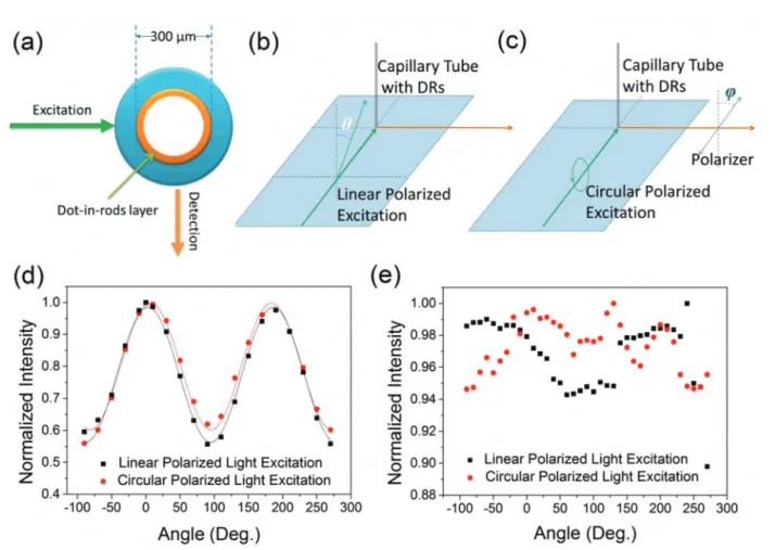
CdSe/CdS DRs were dissolved in hexane (5 mg mL−1), and the solution was loaded into capillary tubes by capillary forces. The capillary tubes with a diameter of 300 μm loaded with the DR solution were dried under reduced pressure or in air. As a result, DRs were deposited on the inner wall of the capil-lary tube. Two methods were employed to verify the optical anisotropy of the DR ensemble in the capillary tubes (Fig. 2). The first method, as illustrated in Fig. 2b, uses a linear polarized laser to excite the sample, and while tuning the polarization angle of the excitation beam with respect to the
capillary tube’s axis, the PL spectra of the DRs loaded in capil-lary are recorded. In the second approach, the sample was excited with a circularly polarized laser, and the polarization of PL was analyzed by varying the angle of the polarizer with respect to the capillary tube’s axis before detection, as shown in Fig. 2c. These two methods are basically used to examine the polarization dependent absorption and emission of the CdSe/CdS DR ensemble in a capillary tube by varying the exci-tation and emission detection polarization angles, respectively. If the DRs are randomly oriented, i.e., their dipole moments are evenly distributed at all angles, the absorption and emis-sion of the CdSe/CdS DR ensemble will not be polarization dependent. Fig. 2d presents the PL intensity of the DR ensem-ble as a function of excitation and emission detection polari-zation angles with respect to the capillary tube’s axis corresponding to the two experiments. The results show that the preferable orientation for polarization of both absorption and emission is parallel to the capillary tube’s axis. The same measurements were applied to the spherical nanocrystal ensemble in a capillary, as shown in Fig. 2e. Polarization dependent absorption and emission for spherical nanocrystals
Fig. 2 Two approaches that were adopted for anisotropic absorption and emission measurements. (a) Cross section of a capillary tube with a dried CdSe/CdS DR layer on its inner wall. (b) Excitation by linear polarized light for anisotropic absorption measurement: varying the polarization angle of excitation and monitoring the emission. (c) Excitation by circularly polarized light for anisotropic emission measurement: varying the polarization angle of the polarizer before the detector and monitoring the emission. (d, e) Normalized emission intensity of spontaneous emission as a function of the polarization angle with respect to the capillary tube in the two approaches for a capillary tube loaded with dried CdSe/CdS DRs (d) and CdSeS/ZnS spherical nanocrystals (e).
Open Access Article. Published on 16 March 2015. Downloaded on 28/08/2017 14:05:58.
This article is licensed under a
dried in a capillary tube are negligible as compared to that of DRs. In addition, the anisotropic behavior was observed when the microcavity was broken by cracking the capillary tubes (Fig. S3†). Hence, any effect of the cylindrical microcavity on the anisotropic optical properties is ruled out, similarly to other reports about a large cylindrical microcavity.32The data points were well fitted with the cosine-squared function of polarization angle (Fig. 2d): cos2θ, where θ is the angle between the capillary tube axis and the polarization of exci-tation or emission corresponding to our first or second method. The polarization ratio to characterize the degree of optical anisotropy of the DR ensemble in capillary tubes is defined as p = (Ik− I⊥)/(Ik+ I⊥), where Ikand I⊥are the
intensi-ties of PL emission with polarization of excitation (or emis-sion) parallel and perpendicular to the capillary tube, respectively. The polarization ratios calculated based on the fitting curves in Fig. 2d are 0.252 and 0.296 for emission and absorption, respectively. As shown above, individual CdSe/CdS DRs demonstrate the highest transition probability of absorp-tion and emission along their c-axis; the high polarizaabsorp-tion ratios of the DR ensemble indicate that the DRs have a prefer-able orientation along the capillary tube. This is also statisti-cally illustrated by scanning electron microscopy (SEM) images of the sample as shown in Fig. S4.†
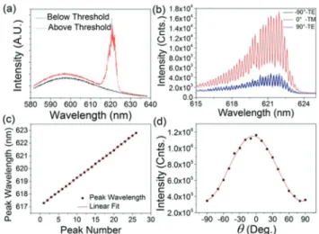
Furthermore, the collective effects with stimulated emission of the aligned DRs in the capillary tubes were investigated. A more concentrated (10 mg mL−1) CdSe/CdS DRs solution was loaded into the capillary tube to deposit onto the inner wall of capillary tubes a preferable film for stimulated emission. The circularly polarized laser, generated from a frequency-doubled Nd:YAG pulsed laser at 532 nm with a repetition rate of 60 Hz and a pulse width of 1 ns and a quarter-wave plate, was used to excite the sample, and the emission anisotropy was exam-ined by varying the polarizer before detection, as shown in Fig. 2c. Under low excitation energy, the emission from the sample was observed as spontaneous emission with a full width at half maximum (FWHM) of about 34 nm, which is similar to those in the above experiments. Increasing the pump energy above the threshold, the emission spectrum became narrow and series of spiky peaks emerged, as shown in Fig. 3a. Closely investigating the lasing peaks (Fig. 3b), the
peaks that are equally spaced with δλ = 0.21 nm can be
resolved (Fig. 3c). The difference in δλ between the TE mode (where the electric field is perpendicular to the tube axis, i.e., −90° or 90°) and the TM mode (where the electric field is par-allel to the tube axis, i.e., 0°) is negligible. These well resolved lasing modes also suggest the optically smooth gain medium with negligible scattering, which is consistent with the SEM image of the CdSe/CdS DR layer on the inner wall of capillary tubes (Fig. S4d†). As seen from a comparison given in ESI Fig. S5,† the mode spacing (δλ) in the similar lasing structure with a smaller capillary tube diameter of 100 μm is δλ = 0.59 nm, three times that at 300μm capillary tube diameter. This result confirms the WGMs in our cylindrical micro-cavities. For WGMs,δλ = λ2/(2πnR), where the center emission wavelength isλ = 620 nm and the capillary tube radius is R =
150 µm, so the effective refractive index n is about 1.92. Such a high refractive index suggests that the lasing modes had a large overlap with closely packed CdSe/CdS DR layers. The high refractive index contrast between the dense semiconduc-tor nanocrystal layers and the glass as compared with that between the organic solvent and glass creates a desired laser configuration where the overlapping between optical modes and the gain medium can be maximized. Fig. 3b also shows the different intensities of lasing spectra in TM and TE modes. As we can see, the lasing intensity in TM mode was much higher than that of TE mode lasing. The lasing intensity, inte-gral of all the lasing peaks from 615 to 625 nm, as a function of the polarization angle was measured and is shown in Fig. 3d under 7 µJ pump energy. As a comparison, the same measurement was conducted with spherical CdSeS/ZnS nano-crystals dried in capillary tubes, as shown in Fig. S6,† and the emission normal to the capillary tube was slightly stronger than that along the capillary. This is due to the fact that the light which is polarized normal to the axis of the capillary tube is more likely to be transmitted out. The results show that the anisotropy of lasing emission in our laser configuration resulted from aligned DRs.
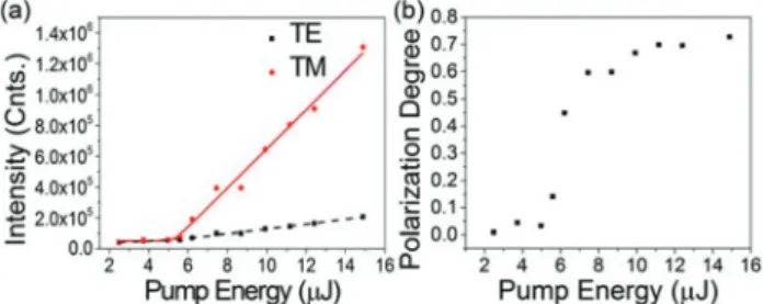
Fig. 4a presents the power transfer functions measured for TE and TM modes of our laser structure. The results are well consistent with “soft threshold” approximation,35 and the threshold was about 5.2 µJ for both TE and TM modes. As can be seen, initially the difference in lasing intensity between these two modes is small and then grows with increasing pumping energy. The evolution of the polarization ratio, p, as a function of pump energy is plotted in Fig. 4b. The polarization ratio of spontaneous emission started at about 0.05 and as the Fig. 3 Stimulated emission characterization from CdSe/CdS DRs in a capillary tube. (a) Emission of DRs in a capillary tube below and above the lasing threshold. (b) Spectra of lasing pumped by a circularly polar-ized laser from CdSe/CdS DRs in the capillary when the detected polari-zation is along the tube (0°, TM mode) and perpendicular (−90° and 90°, TE mode). (c) Plot of laser peaksversus the peak number and linear fit of the data. (d) Lasing intensity as a function of the detection angle with respect to the capillary tube, andfitted with cos2θ function.
Open Access Article. Published on 16 March 2015. Downloaded on 28/08/2017 14:05:58.
This article is licensed under a
pumping energy increased, the polarization ratio built up and finally saturated at 0.72. Here, we notice the polarization ratio reduction in spontaneous emission of this thicker DR film in comparison with that in Fig. 3. The increase of reabsorption in a thicker film could be the main reason for this polarization ratio reduction. However, a majority of CdSe/CdS DRs are oriented along the capillary tube, creating a polarized gain medium with a higher gain coefficient for amplifying light with the electric vector along the tube. The small anisotropy of spon-taneous emission is amplified in the polarized gain medium36 and resulted in a very large polarization ratio, p = 0.72.
Conclusions
In summary, we demonstrated for the first time the utilization of the intrinsic optical anisotropy of CdSe/CdS DRs on a large scale for both spontaneous and stimulated emissions. Evapor-ating a CdSe/CdS DR solution inside a capillary tube leaves a thin film of aligned DRs on the inner wall of the tube. The polarization ratios of spontaneous absorption and emission for aligned DR films are 0.296 and 0.252, respectively, while the WGM lasing resulting from the cylindrical microcavity has the maximum polarization ratio of 0.72. Capillary tubes, after sealing in inert gas, also serve as oxygen and moisture free containers for CdSe/CdS DRs. Therefore, the lifetime and stability of these lasers can be much improved. Recently, LCD TVs were developed with nanocrystals in capillary tubes as the color convertors.37 Given that stimulated emission at red, green and blue colors can be observed from CdSe/CdS DRs,17 our approach with the capillary tubes demonstrating laser emission with a high polarization ratio could be used for novel display backlighting and laser lighting applications.38
Experimental methods
Synthesis of CdSe/CdS dot-in-rods
The synthesis approach is adopted from the literature.13For CdSe seed synthesis, 3 g trioctylphosphine oxide (TOPO), 280 mg octadecylphosphonic acid (ODPA), and 60 mg
cadmium oxide (CdO) were added into a 50 mL three-neck flask. Subsequently the mixture was degased at 150 °C for 2 h. As the temperature was increased under an Ar atmosphere, 1.8 mL trioctylphosphine (TOP) was added after CdO dissolved completely. 58 mg selenium in 0.36 g TOP was injected when the temperature reached 380 °C. Then the flask was removed from the heat mantle intermediately. As for the seeded nanorod growth, 3 g TOPO, 290 mg ODPA, 80 mg hexylphos-phonic acid (HPA) and 86 mg CdO were degased under vacuum for 2 h in a three-neck flask at 150 °C. 1.8 mL TOP was added into the reaction vessel after the mixture became trans-parent, and then 200 µl CdSe seeds (400 µM in TOP) together with 120 mg sulfur in 1.5 g TOP were injected swiftly at 350 °C. The as-synthesized CdSe/CdS DRs were cleaned with acetone and methanol, and then dissolved in hexane.
Wurtzite and zinc blende spherical nanocrystals were syn-thesized using one-pot39 and successive ion layer adsorption and reaction (SILAR)40methods, respectively.
Optical characterization
Absorption and PL spectra were recorded using UV-1800 Shi-madzu and RF-5301 PC. A continuous wave frequency doubled Nd:YAG laser at 532 nm was used for anisotropic optical prop-erty measurements of the DR solution and loaded in capillary tubes. For lasing characterization, the sample was pumped by a frequency doubled Nd:YAG pulsed laser at 532 nm, whose repetition rate is 60 Hz and pulse width is 1 ns. Meanwhile, the polarization response of the detector was measured and corrected, and the detection system shows very good polari-zation insensitivity (Fig. S7†).
Acknowledgements
The authors would like to thank the financial support from
Singapore National Research Foundation under
NRF-RF-2009–09 and NRF-CRP-6–2010–02 and the Science and Engineering Research Council, Agency for Science, Technology and Research (A*STAR) of Singapore ( project no. 092 101 0057 and 112 120 2009). The electron microscopy imaging was per-formed at the Facility for Analysis, Characterization, Testing and Simulation (FACTS) in Nanyang Technological University, Singapore. HVD also gratefully thanks TUBA and EURYI.
Notes and references
1 M. Bruchez, M. Moronne, P. Gin, S. Weiss and
A. P. Alivisatos, Science, 1998, 281, 2013–2016.
2 J. Caruge, J. Halpert, V. Wood, V. Bulović and M. Bawendi, Nat. Photonics, 2008, 2, 247–250.
3 E. H. Sargent, Nat. Photonics, 2012, 6, 133–135.
4 V. Klimov, A. Mikhailovsky, S. Xu, A. Malko,
J. Hollingsworth, C. Leatherdale, H.-J. Eisler and
M. Bawendi, Science, 2000, 290, 314–317. Fig. 4 Power transfer function of CdSe/CdS DRs in a capillary tube. (a)
With increasing the pump energy, the evolution of lasing intensity, inte-gral of all the lasing peaks, for TE and TM WGMs lasing, respectively. (d) Polarization ratio as a function of pump energy.
Open Access Article. Published on 16 March 2015. Downloaded on 28/08/2017 14:05:58.
This article is licensed under a
5 J. Q. Grim, S. Christodoulou, F. Di Stasio, R. Krahne, R. Cingolani, L. Manna and I. Moreels, Nat. Nanotechnol., 2014, 9, 891–895.
6 D. V. Talapin, J.-S. Lee, M. V. Kovalenko and
E. V. Shevchenko, Chem. Rev., 2009, 110, 389–458.
7 T. Erdem and H. V. Demir, Nat. Photonics, 2011, 5, 126– 126.
8 Y. V. Vandyshev, V. Dneprovskii and V. Klimov, JETP Lett., 1991, 53, 314.
9 V. Klimov, A. Mikhailovsky, D. McBranch, C. Leatherdale and M. Bawendi, Science, 2000, 287, 1011–1013.
10 F. García-Santamaría, Y. Chen, J. Vela, R. D. Schaller, J. A. Hollingsworth and V. I. Klimov, Nano Lett., 2009, 9, 3482–3488.
11 L.-W. Wang, M. Califano, A. Zunger and A. Franceschetti, Phys. Rev. Lett., 2003, 91, 056404.
12 V. I. Klimov, S. A. Ivanov, J. Nanda, M. Achermann, I. Bezel, J. A. McGuire and A. Piryatinski, Nature, 2007, 447, 441– 446.
13 L. Carbone, C. Nobile, M. De Giorgi, F. D. Sala, G. Morello,
P. Pompa, M. Hytch, E. Snoeck, A. Fiore and
I. R. Franchini, Nano Lett., 2007, 7, 2942–2950.
14 B. Guzelturk, Y. Kelestemur, M. Z. Akgul, V. K. Sharma and H. V. Demir, J. Phys. Chem. Lett., 2014, 5, 2214–2218. 15 B. Guzelturk, Y. Kelestemur, M. Olutas, S. Delikanli and
H. V. Demir, ACS Nano, 2014, 8, 6599–6605.
16 Y. Kelestemur, A. F. Cihan, B. Güzeltürk and H. V. Demir, Nanoscale, 2014, 6, 8509–8514.
17 I. Moreels, G. Rainò, R. Gomes, Z. Hens, T. Stöferle and R. F. Mahrt, Adv. Mater., 2012, 24, OP231–OP235.
18 C. Grivas, C. Li, P. Andreakou, P. Wang, M. Ding, G. Brambilla, L. Manna and P. Lagoudakis, Nat. Commun., 2013, 4.
19 M. Zavelani-Rossi, M. G. Lupo, F. Tassone, L. Manna and G. Lanzani, Nano Lett., 2010, 10, 3142–3150.
20 Y. Wang, V. D. Ta, Y. Gao, T. C. He, R. Chen, E. Mutlugun, H. V. Demir and H. D. Sun, Adv. Mater., 2014, 26, 2954– 2961.
21 M. Zavelani-Rossi, M. G. Lupo, R. Krahne, L. Manna and G. Lanzani, Nanoscale, 2010, 2, 931–935.
22 F. Pisanello, G. Leménager, L. Martiradonna, L. Carbone, S. Vezzoli, P. Desfonds, P. D. Cozzoli, J.-P. Hermier, E. Giacobino, R. Cingolani, M. De Vittorio and A. Bramati, Adv. Mater., 2013, 25, 1974–1980.
23 J. Hu, L.-s. Li, W. Yang, L. Manna, L.-w. Wang and A. P. Alivisatos, Science, 2001, 292, 2060–2063.
24 J. S. Kamal, R. Gomes, Z. Hens, M. Karvar, K. Neyts, S. Compernolle and F. Vanhaecke, Phys. Rev. B: Condens. Matter, 2012, 85, 035126.
25 F. Pisanello, L. Martiradonna, G. Leménager, P. Spinicelli,
A. Fiore, L. Manna, J.-P. Hermier, R. Cingolani,
E. Giacobino and M. De Vittorio, Appl. Phys. Lett., 2010, 96, 033101.
26 A. Sitt, A. Salant, G. Menagen and U. Banin, Nano Lett., 2011, 11, 2054–2060.
27 A. Rizzo, C. Nobile, M. Mazzeo, M. D. Giorgi, A. Fiore, L. Carbone, R. Cingolani, L. Manna and G. Gigli, ACS Nano, 2009, 3, 1506–1512.
28 J. L. Baker, A. Widmer-Cooper, M. F. Toney, P. L. Geissler and A. P. Alivisatos, Nano Lett., 2009, 10, 195–201.
29 K. M. Ryan, A. Mastroianni, K. A. Stancil, H. Liu and A. Alivisatos, Nano Lett., 2006, 6, 1479–1482.
30 M. Kazes, D. Y. Lewis, Y. Ebenstein, T. Mokari and U. Banin, Adv. Mater., 2002, 14, 317–321.
31 Y. Wang, K. S. Leck, V. D. Ta, R. Chen, V. Nalla, Y. Gao, T. He, H. V. Demir and H. Sun, Adv. Mater., 2014, 27, 169– 175.
32 N. Frateschi, A. Kanjamala, A. Levi and T. Tanbun-Ek, Appl. Phys. Lett., 1995, 66, 1859–1861.
33 M. Grabolle, M. Spieles, V. Lesnyak, N. Gaponik,
A. Eychmüller and U. Resch-Genger, Anal. Chem., 2009, 81, 6285–6294.
34 G. Xing, Y. Liao, X. Wu, S. Chakrabortty, X. Liu, E. K. Yeow, Y. Chan and T. C. Sum, ACS Nano, 2012, 6, 10835–10844. 35 J. Herrnsdorf, B. Guilhabert, Y. Chen, A. Kanibolotsky,
A. Mackintosh, R. Pethrick, P. Skabara, E. Gu, N. Laurand and M. Dawson, Opt. Express, 2010, 18, 25535–25545. 36 B. E. A. Saleh and M. C. Teich, Fundamentals of Photonics,
Wiley, 2013.
37 R. J. Nick, C. A. BREEN, C. M. Denton, S. Sadasivan and J. R. Linton, Google Patents, 2014.
38 A. Neumann, J. J. Wierer, W. Davis, Y. Ohno, S. R. Brueck and J. Y. Tsao, Opt. Express, 2011, 19, A982–A990.
39 W. K. Bae, J. Kwak, J. Lim, D. Lee, M. K. Nam, K. Char, C. Lee and S. Lee, Nano Lett., 2010, 10, 2368–2373.
40 O. Chen, J. Zhao, V. P. Chauhan, J. Cui, C. Wong, D. K. Harris, H. Wei, H.-S. Han, D. Fukumura and R. K. Jain, Nat. Mater., 2013, 12, 445–451.
Open Access Article. Published on 16 March 2015. Downloaded on 28/08/2017 14:05:58.
This article is licensed under a