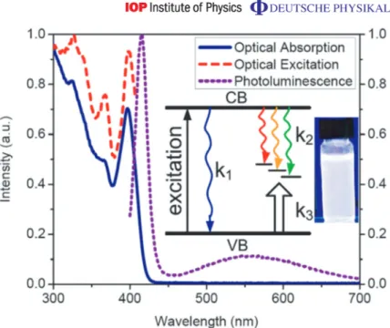
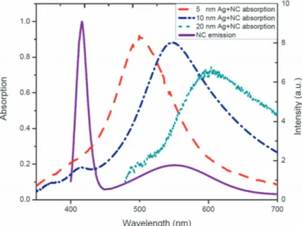
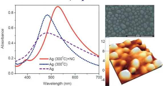
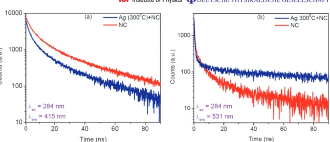
Selective enhancement of surface-state emission and simultaneous quenching of interband transition in white-luminophor CdS nanocrystals using localized plasmon coupling
Tam metin
Şekil

Benzer Belgeler
Although it was initially envisaged that members would gradually form a free trade zone which would possibly evolve into a stronger form of integration, it was later agreed that
[54] A. Dietrich, “Critical casimir forces between spherical particles in fluids,” Phys. Dietrich, “Critical casimir interaction of ellip- soidal colloids with a planar wall,”
Comparison of Optimal Forcing Frequency and PP Control In the preceding section we have illustrated how the simple PP controller with proper time delay between the two feedback loops
When us- ing the Fluorlmager or FMBIO fluorescent scanners, alleles were assigned to the fluorescent PCR fragments by visual or software comparison of unknown samples to
The parallel strategy requires the allocation of an available budget to a number of R&D activities, the determination of the number of research teams within each activity and
In order to avoid problems where uA(~A(r)) # r, and so that the extended operators do not interact improperly, we assume each database relation (r, q,. ..), their nested relations,
The experimental data collected shows that while I/O prefetching brings benefits, its effectiveness reduces significantly as the number of CPUs is increased; (ii) identify
Recent studies in monocrystalline semiconductor solar cells are focused on mechanically stacking multiple cells from different materials to increase the power conversion
