High quality single-crystal germanium-on-insulator on bulk Si substrates based on
multistep lateral over-growth with hydrogen annealing
Hyun-Yong Yu, Szu-lin Cheng, Jin-Hong Park, Ali K. Okyay, M. Cengiz Onbaşlı, Burcu Ercan, Yoshio Nishi, and Krishna C. Saraswat
Citation: Appl. Phys. Lett. 97, 063503 (2010); View online: https://doi.org/10.1063/1.3478242
View Table of Contents: http://aip.scitation.org/toc/apl/97/6
Published by the American Institute of Physics
Articles you may be interested in
Defects reduction of Ge epitaxial film in a germanium-on-insulator wafer by annealing in oxygen ambient
APL Materials 3, 016102 (2015); 10.1063/1.4905487
Reduced pressure–chemical vapor deposition of Ge thick layers on Si(001) for 1.3–1.55-µm photodetection
Journal of Applied Physics 95, 5905 (2004); 10.1063/1.1699524
Effects of hydrogen annealing on heteroepitaxial-Ge layers on Si: Surface roughness and electrical quality
Applied Physics Letters 85, 2815 (2004); 10.1063/1.1802381
High quality Ge on Si by epitaxial necking
Applied Physics Letters 76, 3700 (2000); 10.1063/1.126754
High-quality Ge epilayers on Si with low threading-dislocation densities
Applied Physics Letters 75, 2909 (1999); 10.1063/1.125187
High-quality single-crystal Ge on insulator by liquid-phase epitaxy on Si substrates
High quality single-crystal germanium-on-insulator on bulk Si substrates
based on multistep lateral over-growth with hydrogen annealing
Hyun-Yong Yu,1,a兲Szu-lin Cheng,1Jin-Hong Park,1,2Ali K. Okyay,3,4M. Cengiz Onbaşlı,3 Burcu Ercan,2Yoshio Nishi,1and Krishna C. Saraswat1
1
Department of Electrical Engineering, Stanford University, Stanford, California 94305, USA
2
Department of Electronics and Radio Engineering, College of Electronics and Information, Kyung Hee University, Yongin-si/Gyeonggi-do 446-701, Republic of Korea
3
Department of Electrical and Electronics Engineering, Bilkent University, Ankara 06800, Turkey
4
UNAM, Institute of Materials Science and Nanotechnology, Bilkent University, Ankara 06800, Turkey
共Received 21 June 2010; accepted 21 July 2010; published online 9 August 2010兲
Germanium-on-insulator 共GOI兲 is desired for high performance metal-oxide-semiconductor transistors and monolithically integrated optoelectronics. We demonstrate a promising approach to achieve single-crystal defect-free GOI by using lateral over-growth through SiO2 window. The dislocations due to the lattice mismatch are effectively terminated and reduced in SiO2 trench by selective area heteroepitaxy combined with hydrogen annealing. Low defect density of 4⫻106 cm−2 and low surface roughness of 0.7 nm 共root-mean-square兲 on GOI are confirmed by plan-view transmission electron microscopy and atomic force microscopy analysis. In addition, the excellent metal-semiconductor-metal diode electrical characteristics fabricated on this GOI confirm Ge crystal quality. The selectively grown GOI structure can provide the monolithic integration of SiGe based devices on a Si very large scale integration共VLSI兲 platform. © 2010 American Institute
of Physics.
关doi:10.1063/1.3478242兴
Germanium has been considered as a promising material for high performance complementary metal-oxide-semiconductor 共CMOS兲 transistors and optoelectronic applications as it offers much higher and symmetric carrier mobility1–3 and smaller optical band gap ideal
for 1.3– 1.5 m wavelength commonly used in
telecommunication.4 Germanium-on-insulator 共GOI兲 can specially provide high performance MOS field-effect transis-tors by high-speed operation as well as low parasitic capaci-tance and immunity for short channel effects. Low-leakage junction current by thin-body GOI is also another benefit for channel materials with smaller band gap.5,6 Even more re-search efforts are directed toward the realization of on-chip optical signaling using Ge-based devices. There has been a surge in interest in SiGe based optoelectronics such as near IR detectors,7–9 Ge-based integrated optical modulators,10,11 and so on. The marriage of microelectronics to high performance photonics requires precise control and process compatibility. It is hence crucial to be able to grow high quality SiGe layers selectively on Si. For GOI struc-tures, currently, many techniques such as oxidation-induced Ge condensation,12 laser annealing,13,14 solid-phase crystallization,15,16 metal-induced lateral crystallization,17 bonding,18 and lateral epitaxial growth19 have been intro-duced. However, these techniques to obtain GOI structures can be very complicated and have difficulty in achieving high-quality Ge films. In addition, the monolithic integration with Si based CMOS technology seems to be much more difficult. In other material, such as GaN, lateral overgrowth technique has been demonstrated to effectively reduce dislo-cation densities on GaN films and was used to fabricate very high performance light emitting diodes and laser diodes.20–22
In this paper, we demonstrate the lateral overgrowth of germanium on a SiO2layer with multistep lateral overgrowth with hydrogen annealing 共MLHA兲 technique. This MLHA technique yields Ge layers with very low dislocation density and surface roughness as confirmed by transmission electron microscope 共TEM兲 analysis, and atomic force microscope 共AFM兲 surface morphology studies. In addition, metal-semiconductor-metal 共MSM兲 diode electrical characteristics are shown to confirm Ge crystal quality on SiO2.
A SiO2 layer was thermally grown on p-type 共100兲 Si substrate at 1100 ° C that finally became the insulator layer of the GOI structure. The SiO2 film was then patterned by dry-etching followed by wet-etching. These etched vias be-came the growth windows for selective Ge epitaxy. The start-ing surface is very critical in epitaxy for sstart-ingle-crystal growth; therefore, the samples were etched in 50:1 共H2O : HF兲 for 30 s and immediately loaded into an Applied Materials Centura epitaxial reactor. A hydrogen bake at 1000 ° C was carried out to ensure that no native oxide re-mained on the Si surface between SiO2 walls. In order to increase the resulting films quality, a very thin Si epilayer was first grown for 90 s at 700 ° C with dichlorosilane as the reaction species.
Ge growth on Si is surface reaction limited below 450 ° C and is mass transport limited above.23Therefore, low growth temperatures and pressures provide better selectivity between Si and SiO2. The reaction temperature was found to influence the growth rates of different crystal directions, as reported elsewhere.24At 400 ° C,具100典 normal direction was dominant at 30 nm/min compared to 3 nm/min in 具113典 di-rection. This resulted in facet formation with兵113其 surfaces. At elevated temperatures such as 600 ° C, growth rates for 具100典 and 具113典 directions were 60 nm/min and 12 nm/min, respectively. Therefore, a careful design of the growth con-a兲Electronic mail: [email protected].
APPLIED PHYSICS LETTERS 97, 063503共2010兲
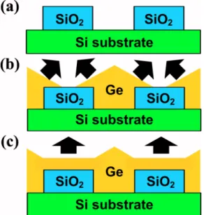
ditions and a trade off between nucleation/selectivity and growth rate is required to achieve high quality GOI virtual substrates. Figure1shows the schematic of the lateral over-growth Ge process. As shown Fig. 1共a兲, an initial low-temperature growth is performed for higher Si– SiO2 selec-tivity and reduced surface roughness. Once Ge layer becomes pyramidlike shape in the SiO2 trench,具311典 direc-tion growth becomes dominant before coalescences in Fig. 1共b兲. After the coalescence happens,具100典 direction growth starts at the valley where two Ge growth fronts meet at spe-cific condition. As shown in Fig.1共c兲, due to a higher growth rate of 具100典 direction compared to that of 具311典 direction, the valley is quickly filled up and具100典 growth is dominant. The initial Ge layer was grown at 400 ° C with a partial pressure of 8 Pa. Temperature in the chamber was raised to 825 ° C and the sample was annealed for 30 min in H2 am-bient. This step is crucial to allow for surface reconstruction, reduce dislocation density and surface roughness.23,25 An
scanning electron microscopy 共SEM兲 image of the sample after this step is shown in Fig.2共a兲. After the coalescence, an additional growth step was performed at 600 ° C for 15 min followed by H2 annealing at 825 ° C, where the valley was filled up due to fast 具100典 direction growth. However, as shown in Fig. 2共d兲,具100典 direction growth does not start at the valley after the coalescence of Ge films at 400 ° C addi-tional growth step. Figure 2共b兲 shows the resulting lateral over-lateral growth with the 400 ° C and 600 ° C growth temperature combination. The overall Ge layer thickness can be increased by longer growth at 600 ° C as demonstrated in Fig.2共c兲for a growth time of 35 min.
Large surface roughness and dislocation density are ob-served on as-grown samples as a result of the 4.2% lattice mismatch between Si and Ge. The surface roughness reduc-tion by annealing in hydrogen ambient at 825 ° C is attrib-uted to hydrogen-mediated Ge diffusion and the reconstruc-tion of the surface.23Figure3shows 40⫻10 m2AFM scan images for two lateral overgrowth Ge films grown without hydrogen annealing and with MLHA. The surface of the sample with no annealing was significantly smoothened with MLHA. A very low rms surface roughness of 0.7 nm was achieved in MLHA GOI samples down from 3.5 nm for unannealed GOI films.
GOI film quality was investigated by TEM analysis. TEM images in Fig. 4 show very high quality Ge layers obtained on SiO2. Ge film grows selectively through a 500 nm wide window in the SiO2 layer. Defects were found only in the first 60 nm thick region from the Ge and Si interface. Previous efforts to obtain high quality epilayers on
FIG. 2. Cross-sectional SEM images of the film after共a兲 growth at 400 °C, 共b兲 growth at 400 °C followed by 15 min at 600 °C, 共c兲 growth at 400 °C followed by 35 min at 600 ° C, and共d兲 growth at 400 °C for 1 h. FIG. 1. 共Color online兲 Illustration 共a兲 of selective Ge growth at 400 °C on Si through openings in the SiO2film.共b兲 Illustration of the growth mecha-nism at 400 ° C before the films coalesce, 共c兲 growth at 600 °C after coalescence.
FIG. 3. 共Color online兲 AFM scan images of 40⫻10 m2of the resulting thick film after low-temperature共400 °C兲 and high-temperature 共600 °C兲 growth共a兲 with and 共b兲 without intermediate H2anneal steps.
FIG. 4.共Color online兲 共a兲 Cross sectional TEM 共XTEM兲 image of grown Ge film and the SiO2mesa block. Defects and dislocations are in close vicinity of the Ge–Si interface while the rest of the film has very low defect density. 关共b兲 and 共c兲兴 High resolution XTEM images of the Ge film on top of the SiO2mesa and the void, showing defect free GOI layers.
Si required a 500 nm or thicker buffer layers to confine the defects and dislocations.10,26 The hydrogen annealing tech-nique reported in this work increases the surface mobility of Ge atoms leading dislocations to glide to Ge/SiO2. In other word, the SiO2 sidewalls provide sinks for the dislocations. Once the Ge film thickness exceeds the height of the SiO2 trench, the lateral overgrowth of the film results in extremely single-crystal GOI layer. Owing to MLHA, the lateral over-grown Ge layer shows very low defect density, having a threading dislocation density count of ⬃4⫻106 cm−2based on the plan view TEM analysis. Figures 4共b兲 and 4共c兲also show no visible defect where the growth fronts join. This is attributed to dislocation trapping within SiO2 trenches.
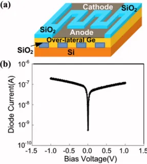
In order to confirm the high crystal quality of Ge layer over-laterally grown on SiO2 electrically, we fabricated simple MSM diode with interdigitated electrode width 共5 m兲 and spacing 共5 m兲 on the top of the over-lateral grown Ge layer. A 200 nm thick low-temperature chemical-vapor-deposited oxide layer was deposited at 400 ° C for the purpose of surface passivation and isolation. This oxide layer was lithographically patterned and HF-etched, followed by metal electrode e-beam evaporation and photoresist lift-off process. Figure 5共a兲 illustrates a schematic diagram of the final structure. 15 nm thick Ti was used for controlling work function as well as achieving good adhesion, and then it was topped with 35 nm thick Au. Figure 5共b兲 presents the electrical current-voltage 共I-V兲 characteristic of MSM 共Ti–Ge–Ti兲 diode. Therefore, high quality Ge layer intro-duces low leakage current.27 Back-to-back Schottky diode behavior and low leakage current of 1.18⫻10−7 A at 1 V as shown in Fig. 5confirms the excellent Ge crystal quality of over-lateral grown GOI substrate.
In conclusion, we have demonstrated very high quality and defect free GOI with MLHA. The multistep 400/600 °C
growth mechanism achieves single-crystal GOI The MLHA. This MLHA technique yields Ge layers with very low dislo-cation density and surface roughness. Such an approach promises the integration of SiGe based devices on a Si very large scale integration 共VLSI兲 platform.
This work was performed at the Stanford Nanofabrica-tion Facility共SNF兲 and was supported by MARCO Intercon-nect Focus Centers and the Stanford University INMP. The authors are grateful to Ted Kamins for helpful discussion.
1C. O. Chui, H. Kim, D. Chi, B. B. Triplett, P. C. McIntyre, and K. C. Saraswat, Tech. Dig. - Int. Electron Devices Meet. 2002, 441.
2C. H. Lee, T. Nishimura, N. Saido, K. Nagashio, K. Kita, and A. Toriumi, Tech. Dig. - Int. Electron Devices Meet. 2009, 457.
3H.-Y. Yu, M. Ishibashi, J.-H. Park, M. Kobayashi, and K. C. Saraswat, IEEE Electron Device Lett. 30, 675共2009兲.
4K. Saraswat, D. Kim, T. Krishnamohan, D. Kuzum, A. Okyay, A. Pethe, and H.-Y. Yu,ECS Trans. 16共10兲, 3 共2008兲.
5S.-I. Takagi, Dig. Tech. Pap. - Symp. VLSI Technol. 2003, 115. 6T. Maeda, K. Ikeda, S. Nakaharai, T. Tezuka, N. Sugiyama, Y. Moriyama,
and S. Takagi,Thin Solid Films 508, 346共2006兲.
7M. Oehme, J. Werner, E. Kasper, M. Jutzi, and M. Berroth,Appl. Phys. Lett. 89, 071117共2006兲.
8D. Ahn, C. Hong, J. Liu, W. Giziewicz, M. Beals, and L. C. Kimerling, Opt. Express 15, 3916共2007兲.
9H.-Y. Yu, S. Ren, W. S. Jung, A. K. Okyay, D. A. B. Miller, and K. C. Saraswat,IEEE Electron Device Lett. 30, 1161共2009兲.
10Y. H. Kuo, Y. Lee, Y. Ge, S. Ren, J. E. Roth, T. I. Kamins, D. A. B. Miller, and J. S. Harris,Nature共London兲 437, 1334共2005兲.
11O. Fidaner, A. K. Okyay, J. E. Roth, R. K. Schaevitz, Y. H. Kuo, K. C. Saraswat, J. S. Harris, and D. A. B. Miller,IEEE Photonics Technol. Lett.
19, 1631共2007兲.
12S. Nakaharai, T. Tezuka, N. Sugiyama, Y. Moriyama, and S. Takagi,Appl. Phys. Lett. 83, 3516共2003兲.
13H. Watakabe, T. Sameshima, H. Kanno, T. Sadoh, and M. Miyao,J. Appl. Phys. 95, 6457共2004兲.
14W. Yeh, H. Chen, H. Huang, C. Hsiao, and J. Jeng,Appl. Phys. Lett. 93, 094103共2008兲.
15I. Tsunoda, A. Kenjo, T. Sadoh, and M. Miyao,Appl. Surf. Sci. 224, 231 共2004兲.
16C. Y. Tsao, J. W. Weber, P. Campbell, P. I. Widenborg, D. Song, and M. A. Green,Appl. Surf. Sci. 255, 7028共2009兲.
17J.-H. Park, P. Kapur, H. Peng, and K. C. Saraswat,Appl. Phys. Lett. 91, 143107共2007兲.
18M. N. Kamalasanan, S. Chandra, P. C. Joshi, and A. Mansingh, Appl. Phys. Lett. 59, 3547共1991兲.
19V. D. Cammilleri, V. Yam, F. Fossard, C. Renard, D. Bouchier, P. F. Fazzini, L. Ortolani, F. Houdellier, and M. Hytch,Appl. Phys. Lett. 93, 043110共2008兲.
20H. Marchand, X. Wu, J. Ibbetson, P. Fini, P. Kozodoy, S. Keller, J. Speck, S. DenBaars, and U. Mashra,Appl. Phys. Lett. 73, 747共1998兲. 21A. Usui, H. Sunakawa, A. Sakai, and A. Yamaguchi,Jpn. J. Appl. Phys.,
Part 2 36, L899共1997兲.
22S. Nakamura, M. Senoh, S. Nagahama, N. Iwasa, T. Yamada, T. Matsushita, H. Kiyoku, Y. Sugimoto, T. Kozaki, H. Umemoto, M. Sano, and K. Chocho,Jpn. J. Appl. Phys., Part 2 36, L1568共1997兲.
23A. Nayfeh, C. O. Chui, and K. C. Saraswat,Appl. Phys. Lett. 85, 2815 共2004兲.
24J.-S. Park, J. Bai, M. Curtin, B. Adekore, M. Carroll, and A. Lochtefeld, Appl. Phys. Lett. 90, 052113共2007兲.
25S. Kobayashi, M. Cheng, A. Kohlhase, T. Sato, J. Murota, and N. Mikoshiba,J. Cryst. Growth 99, 259共1990兲.
26H. Luan, D. Lim, K. Lee, K. Chen, J. Sandland, K. Wada, and L. Kimerling,Appl. Phys. Lett. 75, 2909共1999兲.
27A. K. Okyay, A. M. Nayfeh, T. Yonehara, A. Marshall, P. C. McIntyre, and K. C. Saraswat,Opt. Lett. 31, 2565共2006兲.
FIG. 5. 共Color online兲 共a兲 Cross-section of MSM diode fabricated on over-lateral grown Ge layer. 共b兲 Current vs voltage characteristics of metal-semiconductor 共Ti–Ge兲 Schottky diode on over-lateral grown GOI, both forward and reverse bias regions.