Semiconductor Science and Technology
PAPER
Effect of gate structures on the DC and RF performance of AlGaN/GaN
HEMTs
To cite this article: Ahmet Toprak et al 2018 Semicond. Sci. Technol. 33 125017
View the article online for updates and enhancements.
Effect of gate structures on the DC and RF
performance of AlGaN
/GaN HEMTs
Ahmet Toprak
1,2, Sinan Osmano
ğlu
1, Mustafa
Öztürk
1, Do
ğan Yılmaz
1,
Ömer Cengiz
1,
Özlem Şen
3, Bayram Bütün
1,
Şadan Özcan
2,4and
Ekmel
Özbay
1,51
Nanotechnology Research Center, Bilkent University, 06800 Ankara, Turkey 2
Department of Nanotechnology and Nanomedicine, Hacettepe University, 06532 Ankara, Turkey 3Filkon Electronic, Üniversiteler Mh., Galyum Blok D:B-05, 06800 Ankara, Turkey
4
Department of Physics Engineering, Hacettepe University, 06800 Beytepe, Ankara, Turkey 5
Department of Electrical and Electronics Engineering, Department of Physics, UNAM-Institute of Materials Science and Nanotechnology, Bilkent University, 06800 Ankara, Turkey
E-mail:[email protected]
Received 6 July 2018, revised 4 October 2018 Accepted for publication 26 October 2018 Published 13 November 2018
Abstract
This work analyzes the effect of various gate structures on the DC and radio frequency(RF) performance of AlGaN/GaN high-electron mobility transistors (HEMTs). AlGaN/GaN HEMT devices with a 3μm drain-to-source spacing, 125 μm gate width and 0.3 μm gate length in various gate structures were fabricated to achieve the desired frequency response with a robust, high yield, and repeatable process. The maximum drain current(IDS,max), maximum DC transconductance(gm), pinch-off voltage (Vth), current-gain cutoff frequency (fT), maximum oscillation frequency(fmax), and RF characteristics of the devices in terms of the small-signal gain and RF output power(Pout) at 8 GHz were investigated. The results showed that the output power is increased by 1 dB when the gate structure is changed fromfield plate to gamma gate. The Vth, gm, fTand fmaxvalues are maximized when the thickness of the passivation layer between the gate foot and the gate head is minimized. It is shown that the IDS,maxis decreased and Pout is increased when the gate recess etching process is performed.
Keywords: AlGaN, GaN, high-electron mobility transistor(HEMT), field plate, gamma gate, recessed gate
(Some figures may appear in colour only in the online journal) 1. Introduction
Gallium-nitride (GaN) based high-electron mobility transis-tors(HEMTs) on SiC devices have attracted much attention for high radio frequency(RF) power applications due to their highly demanded physical and electrical properties, such as high current density, high breakdown voltage, high thermal conductivity, and high saturation velocity compared to GaAs based HEMTs[1–3]. GaN based HEMTs are also suitable for coplanar waveguide(CPW) passive technology [2]. AlGaN/ GaN HEMT technology is relatively new compared to Si and GaAs and there are still difficulties in manufacturing these devices with a robust process for high frequencies and high powers. In this work, we have investigated the effects of the
different types of gate present in the literature for the same epitaxial structure, drain-source distance, gate length, and field plate length, under the same measurement conditions. Previously in the literature, various gate structures such as I-gate or standard gate structure[4], gate connected field plate [5], gamma (Γ) gate [6,7], Γ-gate-recessed structure [8] and Γ-gate with air gap structure [9,10] were investigated. In this work, the structures investigated are named as follows: Type-1 refers to an I-gate, Type-2 refers to an I-gate containing a gate connectedfield plate; Type-3 refers to a SiN-passivated Γ-gate obtained using dry etch techniques, Type-4 refers to a Γ-gate obtained using electron beam lithography methods, and Type-5 refers to aΓ-gate with air gap structure. Wu et al [5] reported that at 8 GHz, an output power density of
Semicond. Sci. Technol. 33(2018) 125017 (7pp) https://doi.org/10.1088/1361-6641/aaebab
30.6 W mm−1, power added efficiency (PAE) of 49.6% and a gain of 10.7 dB at a bias of 120 V were achieved for a gate similar to Type-2 with an LG of 550 nm and LFof 900 nm. Wang et al [8] reported that at 8 GHz, an output power density of 9.05 W mm−1, a PAE of 36.4%, a gain of 5.6 dB, a current gain cut-off frequency of 24 GHz and an maximum oscillation frequency of 34 GHz at a bias of 40 V were achieved for a gate similar to Type-3 with an LGof 350 nm. Pei et al[10] reported that at 10 GHz, an output power density of 3 W mm−1, a PAE of 70% at a bias of 20 V were achieved for a gate similar to Type-5 with an LGof 200 nm.
Although reports on devices containing solelyfield plates or gamma gates exist, a report comparing different gate structures with the same epitaxial structure, drain-source distance, gate length andfield plate length, under the same set of high power and high frequency conditions does not, which we believe is the significance of our report. Maximum drain current, maximum DC transconductance, pinch-off voltage, current-gain cutoff frequency, maximum oscillation fre-quency, small-signal gain, RF output power(at 8 GHz), and efficiency of AlGaN/GaN HEMTs are presented. AlGaN/ GaN HEMTs are fabricated using CPW technology with a 3μm drain-to-source spacing, 125 μm gate width, and 0.3 μm gate(foot) length (LG) in various gate structures to achieve the desired frequency response with a robust, high yield, and repeatable process.
2. Device realization
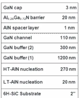
The AlGaN/GaN HEMT structure was grown on a 2′ 6H-SiC substrate in a low-pressure metal-organic chemical vapor deposition reactor (Aixtron 200/4 RF-S). Trimethylgallium (TMGa), trimethylaluminum (TMAl), trimethylindium (TMIn), and ammonia (NH3) were used as Ga, Al, In, and N precursors, respectively. Prior to epitaxial growth, the sub-strate was annealed at 1150°C for 10 min in a hydrogen environment to remove the surface contaminants. The growth of the HEMT structure was initiated with a 20 nm-thick low temperature AlN nucleation layer. Then, a 270 nm thick high temperature (HT) AlN buffer layer was grown at 1150 °C followed by a 1200 nm low pressure carbon doped GaN buffer. Subsequently, a 300 nm thick nominally undoped GaN buffer (2) layer was grown at 1090 °C. After that, a 110 nm high mobility GaN channel was grown at 1120°C at a higher pressure than the carbon doped GaN buffer. Active layers were formed with a 1 nm thick AlN spacer layer and a 20 nm thick undoped AlGaN barrier layer at 1150°C with a 28% Al composition. Epitaxial growth was completed with a 3 nm thick GaN cap layer at the same temperature with the AlGaN barrier[11–19]. The cross-section of the AlGaN/GaN HEMTs on 6H-SiC structure is shown infigure1.
The electrical properties of the two-dimensional electron gas (2DEG) were measured with a contactless microwave Hall effect system. The grown HEMT structure exhibited the 2DEG mobility of 1877 cm2/V.s with a sheet charge density of 1.270×10¹³/cm2 and as low as a 262Ω/sq. sheet resistance at room temperature.
The schematics of AlGaN/GaN HEMTs with various gate structures are given in figure2. Gate head lengths(LH) are designed at 1.1μm to obtain a 0.6 μm field plate length (LF). Gate length (LG), gate to source distance (LGS), and gate to drain distance(LGD) are chosen to be 0.3 μm, 0.8 μm, and 1.9μm, respectively, to achieve a high yield, and repeatable process. The characterized HEMT devices have a 1 mm total gate width in the 8×125 μm configuration.
The fabrication process started with mesa isolation etching and ohmic contact formation for the entire device. Mesa etching was performed with an inductively coupled plasma reactive ion etching (ICP-RIE) system by using Cl2/BCl3 plasma-based dry etch. The mesa’s height was measured as 85 nm by a using surface profilometer. For ohmic contact formation, a Ti/Al/Ni/Au metal stack was deposited by using an electron beam evaporator(EBE) system with the thicknesses of 12, 120, 35, and 65 nm, respectively. The metal stack was annealed in a nitrogen atmosphere at 850°C for 30 s. After ohmic contacts were formed, TLM measurements were completed using the four-point probe method. The measured ohmic contact resistance was 0.2Ω.mm.
Since the gates of all the devices were in different forms, the fabrication steps for gate contact were different for each device.
In order to pattern the gate feet regions of the samples, different fabrication steps were applied. A Type-3 device and Type-5 device were passivated with a 200 nm-thick Si3N4 layer grown by a plasma-enhanced chemical vapor deposition (PECVD) system before the formation of the gate pattern. Then, for only a Type-5 device, 80 nm Germanium (Ge) metal was deposited by using EBE over the passivation layer. Type-1 and Type-2 devices were covered with PMMA 950 K A6, the Type-3 and Type-5 devices were covered with ZEP 520 A, and the Type-4 device was covered with three
Figure 1.Cross sectional structure of the AlGaN/GaN HEMTs on SI 6H-SiC grown by MOCVD.
2
additional layers of electron beam resists, PMMA 950 K A4, MAA EL13 copolymer and then PMMA 50 K A5. Then, in order to define the gate feet, all of the devices were patterned with direct electron-beam lithography with a single exposure. The feet regions of the Type-3 device and Type-5 device were formed by means of dry etching of ICP-RIE with an SF6/Ar gas mixture.
In order to form the gate head pattern, the Type-3 device and Type-5 device were covered with PMMA 950 K A6 and electron beam lithography was used to define the gate heads. For only the Type-4 device, 5 nm recess etching was done by using CI2/BCI3 plasma based dry etch for the Type-4 gate structure.
Thereafter, all of the samples’ gate feet and head regions were deposited with an Ni/Au metal stack by using the EBE system with thicknesses of 50 and 300 nm, respectively. After this step, Ge wet etching was done with a 10% H2O2solution for only the sample with a Type 5 gate structure.
As the next step in fabrication, the devices without a passivation layer, i.e. Type-1, Type-2 and Type-4 devices, were passivated with a 300 nm-thick Si3N4 layer using the PECVD system. Then, the openings, where the field plates and interconnected metals would be deposited, were formed by means of the dry etching of the ICP-RIE system with SF6 and Ar gas mixtures.
After this step the Type-2 device with afield plate had its gate structure covered with ZEP 520 A and patterned with direct electron-beam lithography with a single exposure to define the field plate. Then, these regions were deposited with a Ti/Au metal stack by using the EBE system with thick-nesses of 15 and 340 nm, respectively, for field plate meta-lization formation. SEM images of gate structures are given in figure3.
For all of the devices, the air bridge post structures were constituted to reduce the parasitics between cross-overs and for preventing a short circuit of the metals by functioning as a jumper. Finally, a Ti/Au metal stack with a total thickness of 2.2μm had been deposited as an interconnection using the EBE system, and the fabrication process was completed with this last step. Figure 4 shows a completed device’s optical microscope image.
3. Results
DC measurements were performed using a parametric semi-conductor device analyzer. Figure5 shows the ID-VGS char-acteristics for devices with different gate structures. The pinch off-voltages (Vth) are −3.8 V for the Type-1 device, −3.7 V for the Type-2 device,−3.0 V for the Type-3 device, −3.2 V for the Type-4 device, and−1.9 V for the Type-5 device.
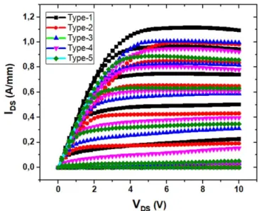
Figure 6 shows the IDS-VDS characteristics for devices with different gate structures. The maximum current densities (IDS,max) are 1.1 A mm−1for the Type-1 device, 1.0 A mm−1 for the Type-2 and Type-3 devices, 0.9 A mm−1for the Type-4 device, and 0.88 A mm−1 for the Type-5 device.
Figure7shows the gm-VGScharacteristics of the devices for different gate structures. The peak transconductance
Figure 2.Schematic of AlGaN/GaN HEMTs with various gate
values for the devices are 0.29 S mm−1for the Type-1 device, 0.25 S mm−1 for the Type-2 device, 0.29 S mm−1 for the Type-3 device, 0.28 S mm−1 for the Type-4 device, and 0.33 S mm−1for the Type-5 device.
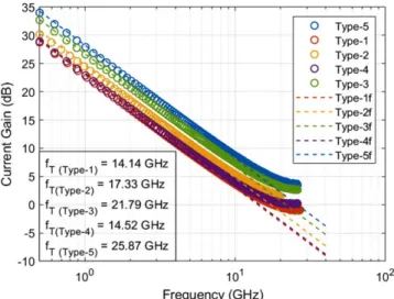
On-wafer small-signal measurements were carried out in the 1–20 GHz frequency range. The devices were biased at drain to source voltage, VDS=25 V and drain to source current IDS=100 mA mm−1. Short-circuit current-gain|h21|
Figure 3.SEM images of gate structures.
Figure 4.Optical microscope image of fabricated HEMTs.
Figure 5.Comparison of the pinch off-voltage(Vth) characteristics of AlGaN/GaN HEMTs with various gate structures.
Figure 6.Comparison of the drain current-voltage(IDS–VDS) characteristics of AlGaN/GaN HEMTs with various gate structures.
4
and Mason’s unilateral power-gain UGwere derived from on-wafer S-parameter measurements as a function of frequency (figures8and9). The unity current-gain cutoff frequencies, fT are 14.14 GHz, 17.33 GHz, 21.79 GHz, 14.52 GHz and 25.87 GHz for the Type-1, Type-2, Type-3, Type-4, and Type-5 devices, respectively. The maximum oscillation fre-quency fmaxare 35.5 GHz, 28.2 GHz, 44.65 GHz, 35.45 GHz and 53.1 GHz for the Type-1, Type-2, Type-3, Type-4, and Type-5 devices, respectively.
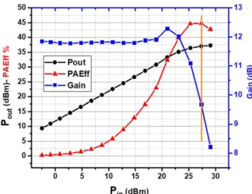
Large-signal measurements were performed using an automated load pull system at 8 GHz. The data were taken on-wafer at room temperature without any thermal management. HEMTs were measured at 100 mA mm−1 drain to source current with 25 V drain bias and the output power, small-signal gain and power added efficiency (PAE) values were obtained (figure 10–14). Small-signal gains are 10.3 dB, 10.3 dB, 9.7 dB, 8.8 dB and 12.7 dB; output powers at 2 dB gain compression are 35.3 dBm (3.4 W mm−1), 36.5 dBm
Figure 7.Comparison of transconductance(gm–VGS) characteristics of AlGaN/GaN HEMTs with the various gate structures.
Figure 8.Comparison of short-circuit current-gain|h21| of AlGaN/ GaN HEMTs with the various gate structures. Devices were biased at VDS=25 V with IDS=100 mA mm−1.
Figure 9.Comparison of Mason’s unilateral power-gain UGof AlGaN/GaN HEMTs with the various gate structures. Devices were biased at VDS=25 V with IDS=100 mA mm−1.
Figure 10.Large-signal performance of AlGaN/GaN HEMTs with
Type-1 gate structures.
Figure 11.Large-signal performance of AlGaN/GaN HEMTs with
(4.5 W mm−1), 37 dBm (5.0 W mm−1), 38.2 dBm (6.6 W mm−1) and 36.7 dBm (4.7 W mm−1); PAE (%) values are 36.8, 44.6, 44.7, 63.1, and 47.1 for the Type-1, Type-2, Type-3, Type-4, and Type-5 devices, respectively. The DC, small-signal and large-signal results are summarized in table1.
4. Conclusion
High-quality AlGaN/GaN HEMTs on a 6H-SiC structure were grown by MOCVD and a study was conducted to examine the effect of various gate structures on the DC and RF performance of AlGaN/GaN HEMTs without using hole technology.
With these measurements, it was seen that the IDS,max value was the highest and Vth value was the smallest in AlGaN/GaN HEMTs with a Type-1 gate structure since the absence of a field plate increases gate resistance [20]. The absence of afield plate also decreases the gate to source and gate to drain capacitances (fringing capacitance, CGF) [21] that limit the decrease in fmax, although fTof a Type-1 device is the lowest, and fmax is not. In addition, this absence of a field plate structure also results in the lowest output power density and lowest power added efficiency.
For a Type-2 device, the gate connected field plate structure decreases gate resistance and intrinsic gate capaci-tance(CGO) which results in the lowest gm. However, thefield plate structure increases the intrinsic electron velocity (νe) [22] which limits the decrease in the fT, but the passivation layer between the gate and field plate increases the CGF considerably and results in the lowest fmax [21]. This field plate structure increases the output power and efficiency compared to a Type-1 device[5].
In a Type-3 device, the gamma gate structure increases the Vth, and gmand maintains the same IDS,maxcompared to Type-2. This means that the gate resistance is smaller and CGOis bigger than Type-2. The passivation between the gate head and foot that decreases the CGFcompared to Type-1 and results in higher fT and fmax. The output power at 2 dB
Figure 12.Large-signal performance of AlGaN/GaN HEMTs with the Type-3 gate structures.
Figure 13.Large-signal performance of AlGaN/GaN HEMTs with the Type-4 gate structures.
Figure 14.Large-signal performance of AlGaN/GaN HEMTs with
the Type-5 gate structures.
Table 1.Summary of the results of the AlGaN/GaN HEMTs devices with the various gate structures.
Gate Structure Type-1 Type-2 Type-3 Type-4 Type-5 IDS,max (A mm−1) 1.1 1.0 1.0 0.9 0.88 Vth(V) −3.8 −3.7 −3.0 −3.2 −1.9 gm(S mm−1) 0.29 0.25 0.29 0.28 0.33 fT(GHz) 14.14 17.33 21.79 14.52 25.87 fmax(GHz) 35.5 28.2 44.65 35.45 53.1 PAEa(%) 36.8 44.6 44.7 63.1 47.1 Gaina(dB) 10.3 10.3 9.7 8.8 12.7 Output Pow-era(dBm) 35.3 36.5 37 38.2 36.7 Output Powera (W mm−1) 3.4 4.5 5.0 6.6 4.7 a At 25 V, 2 dB comp. 6
compression of a Type-3 device is higher than Type-2 since the CGFis smaller and the lack of a passivation layer above the gate head results in better thermal performance, leading to higher output power.
A Type-4 device is the most preferable when the output power and efficiency are considered. It is observed that a 2 nm recess etched process into the the AlGaN barrier layer and placing the Schottky gate directly on the AlGaN barrier layer decreases the CGO, results in smaller gm, and increases gate resistance, resulting in the small Vthcompared to a Type-3 device. Recess process[23] and the passivation layer over the gate increases CGF, which results in smaller fTand fmax compared to a Type-3 device. The recess process and the passivation over the gate head can be a good alternative in the HEMT fabrication process due to the power performance.
A Type-5 device has the highest Vth, gm, small-signal gain, fTand fmaxvalue due to the air under the gate head and above the passivation layer (owing to the lowest CGF and highest CGOcompared to other the gate types) [21,22]. This fabrication process is a good alternative to increase the high frequency performance of HEMTs without limiting the power performance. It is possible to have high fT and fmax values without decreasing the gate length and without decreasing the power performance.
The DC and RF performance of HEMTs devices are strictly dependent on the gate structure. The gate structure and fabrication process should be optimized considering the requirements, robustness and ease of fabrication. Type-4 devices seem to be the best when power and efficiency are considered. Type-5 seems the best alternative when operating at a higher small-signal gain without the reduction of power performance being an issue and, in this way, the fmaxvalue increases with a considerably long gate length and the process is robust and repeatable.
Acknowledgments
One of the authors(E O) acknowledges partial support from the Turkish Academy of Sciences.
ORCID iDs
Ahmet Toprak https://orcid.org/0000-0003-4879-8296
Bayram Bütün https://orcid.org/0000-0003-0892-4681
References
[1] Shur M S 1998 Solid-State Electron.42 2131–8
[2] Mishra U K, Shen L, Kazior T E and Wu Y F 2008 Proc. IEEE
96 287–305
[3] Roccaforte F, Fiorenza P, Greco G, Nigro R L, Giannazzo F, Lucolano F and Saggio M 2018 Microelectron. Eng.
187–188 66–77
[4] Shealy J R, Kaper V, Tilak V, Prunty T, Smart J A, Green B and Eastman L F 2002 J. Phys.: Condens. Matter
14 3499
[5] Wu Y-F, Saxler A, Moore M, Smith R P, Sheppard S, Chavarkar P M, Wisleder T, Mishra U K and Parikh P 2004 IEEE Electron Device Lett.25 117–9
[6] Kumar V, Chen G, Guo S and Adesida I 2006 IEEE Trans. Electron Devices53 1477–80
[7] Lin C K, Wang W-K, Hwu M-J and Chan Y–J 2004 J. Vac. Sci. Technol. B22 1723–6
[8] Wang X L, Chen T S, Xiao H L, Wang C M, Hu G X, Luo W J, Tang J, Guo L C and Li J M 2008 Solid-State Electron.52 926–9
[9] Palaciosa T, Snow E, Pei Y, Chakraborty A, Keller S, DenBaars S P and Mishra U K 2005 IEEE Int. Electron Devices Meeting(https://doi.org/10.1109/
IEDM.2005.1609472)
[10] Pei Y, Poblenz C, Corrion A L, Chu R, Shen L, Speck J S and Mishra U K 2008 Electron. Lett.44 (9) 1-2
[11] Amano H, Sawaki N, Akasaki I and Toyoda Y 1986 Appl. Phys. Lett.48 353–5
[12] Lo C-F et al 2012 J. Vac. Sci. Technol. B30 (1) 011205
[13] Arslan E, Öztürk M K, Tıraş E, Tıraş T, Özçelik S and Özbay E 2017 J. Mater. Sci. Mater. Electron.28 3200–9 [14] Wang X L et al 2005 Solid-State Electron.49 1387–90
[15] Jiménez A et al 2003 Appl. Phys. Lett.82 (26) 4827–9
[16] Guo L et al 2008 Microelectron. J.39 777–81
[17] Tilak V et al 2001 IEEE Electron Device Lett.22
[18] Miyoshi M et al 2004 Japanese J. Appl. Phys.43 7939–43
[19] Waltereit P et al 2009 J. Appl. Phys.106 (2) 023535
[20] Greco G, Lucolano F and Roccaforte F 2018 Mater. Sci. Semicon. Proc.78 96–106
[21] Jessen G H, Fitch R C, Gillespie J K, Via G, Crespo A, Langley D, Denninghoff D J, Trejo M and Heller E R 2007 IEEE Trans. Electron Devices54 2589–97
[22] Guerra D, Saraniti M, Ferry D K, Goodnick S M and Marino F A 2011 IEEE Trans. Electron Devices58 3876–84 [23] Song Bo et al 2014 IEEE Trans. Electron Devices61 747–54