Band alignment issues related to HfO
2/ SiO
2/
p-Si gate stacks
S. Sayan, T. Emge, and E. Garfunkela)
Department of Chemistry, Rutgers University, Piscataway, New Jersey 08854
Xinyuan Zhao, L. Wielunski, R. A. Bartynski, and David Vanderbilt
Department of Physics and Astronomy, Rutgers University, Piscataway, New Jersey 08854
J. S. Suehle
Semiconductor Electronics Division, National Institute of Standards and Technology, Gaithersburg, Maryland 20899
S. Suzer
Department of Chemistry, Bilkent University, 06533 Ankara, Turkey
M. Banaszak-Holl
Department of Chemistry, University of Michigan, Ann Arbor, Michigan 48109
(Received 12 February 2004; accepted 4 August 2004)
The valence and conduction band densities of states for the HfO2/ SiO2/ Si structure are determined
by soft x-ray photoemission and inverse photoemission. First principles calculations are used to help in assigning valence band maxima and conduction band minima. The energies of defect states at the band edges are estimated by comparing the theoretical and experimental results. Determinations of the local surface potentials before and after a forming gas anneal are used to help determine the possible location of the charge in the film. © 2004 American Institute of Physics.
[DOI: 10.1063/1.1803107] I. INTRODUCTION
The need for a high permittivity (high-k) material for future nanoelectronic devices is clear.1To replace SiO2 with
a high-k dielectric, one of many requirements is that both valence and conduction band offsets of the material (with respect to the silicon band edges) need to be greater than 1 eV.2 Although many reports of high-k / silicon gate stack structures have appeared, most of which explore HfO2 and
ZrO2based materials, a consensus on the best dielectric
ma-terial has yet to be reached.
Recently we have reported that the electronic structures
(including energy gap, band offsets, charge neutrality level,
and permittivity…) of these materials are strongly phase
(crystal structure) dependent.3,4,28
Thus the crystal structure of this class of high-k dielectrics should be reported along with any experimental data if a valid comparison of results from different experimental techniques is desired. In this study, we examine HfO2 deposited on SiOxNy/ p-Si by
pho-toemission spectroscopy (PES) and inverse photoemission spectroscopy(IPES). The experimental determination of va-lence band maxima (VBM) and conduction band minima
(CBM) remains a controversial issue. The reports of high-k
materials on silicon using photoemission and optical meth-ods usually employ a “straight-line” method where the va-lence and conduction edges are determined using a linear extrapolation of the data to the “background” intensity level. Although this particular method does not have a strong physical justification(the band shape is part of the intrinsic nature of the material and is rarely “straight”), it serves as a common method for all in the field to compare their work. In
general, polycrystalline semiconductors present a higher con-centration of defects and imperfections than bulk single crys-tals. The presence of structural disorder can also be related to deviations from ideal stoichiometry and/or impurities. One major consequence is that new electronic states may appear which manifest themselves as increased densities of states in the vicinity of the band edges; these are sometimes called band tail states.5 The presence of band tail states not only reduces the observed gap but it may increase carrier transport across or scattering in (or near) the dielectric. The defect bands may also overlap with the bands of the perfect crystal.6 The experimentally observed density of states(DOS) can be considered as a superposition of the perfect crystal DOS and defect bands. A change in the band edge would change the offset assignments and lead to a reduced “effective gap.” The exact value of an intrinsic energy gap has yet to be deter-mined for an ultrathin crystalline dielectric film since all high-k films reported to date are either polycrystalline or amorphous and have crystal imperfections (defects) which inevitably contribute to the electronic properties. What are needed are careful measurements of bulk single crystals and crystalline ultrathin films to confirm theoretical predictions, a goal yet to be realized for this class of oxides.
Electronic states can appear either near the edges or closer to midgap that can be either structural or composi-tional in nature(e.g., metal or oxygen vacancy).7The charge neutrality level (CNL) of these states with respect to the Fermi energy will determine their occupancy and charge, as well as their effect on the band alignment. The rate at which the occupancy of these states change as the electrode volt-ages are varied, will depend on their distance from the elec-trode and other defects, as well as their energy, and may be critical in determining device electrical characteristics. a)Electronic mail: [email protected]
II. EXPERIMENT
HfO2 films were deposited on 11 Å SiOxNy/ p-Si at
⬃400 °C using chemical vapor deposition, with
Hf-tetra-tert-butoxide as the precursor; details of the growth can be found elsewhere.8The primary substrate used in the studies reported here was p-type Si(100) with a doping concentra-tion of ⬃1⫻1015 cm−3. The thickness of the SiO
xNy film
was 11 Å as measured by medium energy ion scattering
(MEIS), and the O:N ratio in the oxynitride was⬃4:1. By
MEIS, the stoichiometry of the as-deposited overlayer was determined to be HfO2.17±0.06. The work reported in this
pa-per used HfO2films of 10 – 30 Å and up to 1000 Å for x-ray
diffraction (XRD) measurements. The forming gas anneals were done at 400 ° C and 1 Torr forming gas pressure(5% H2/ Ar). Soft x-ray photoemission measurements were
per-formed at Brookhaven National Laboratories on the U8B beamline using 120– 400 eV photon energies. The inverse photoemission studies were performed in fluorescence mode in the 18 – 22 eV electron energy range at Rutgers University. The x-ray photoelectron spectroscopy measurements were performed on a Kratos XSAM 800 utilizing Mg K␣
共1253.6 eV兲 as the excitation photon energy.
Rutherford backscattering spectroscopy(RBS) measure-ments are done using a 2 MeV He++beam. The wide-angle x-ray scattering patterns of several samples of HfO2thin
lay-ers on Si substrates were obtained using a Bruker HiStar area detector and an Enraf-Nonius FR571 rotating anode x-ray generator equipped with a graphite monochromator(Cu K␣;
=1.5418 Å) operating at 40 kV and 50 mA. The sample to
detector distance was 5.5 cm and the standard spatial calibra-tion was performed at that distance. Scans were 3 deg wide in omega 共兲 with fixed detector, or Bragg, angle 共2兲 of 40 deg, and fixed platform(and) angles of 0 and 0 deg, respectively. In all cases, the count rate for the area detector did not exceed 100 000 cps.
III. RESULTS AND DISCUSSION A. PES and IPES measurements
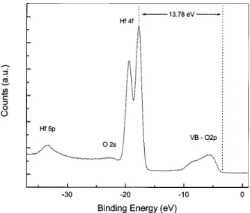
Figure 1 shows the photoemission spectra and peak as-signments in the valence band region for a 28 Å HfO2/ SiOxNy/ p-Si gate stack. The intense feature in the
17– 20 eV region is the Hf 4f spin-orbit doublet. The curve fitting was performed after a Shirley background subtraction. A pair of Gaussians was used to model this region represent-ing the spin-orbit splittrepresent-ing of the 4f level. The spin-orbit splitting was found to be 1.66 eV. The intensity ratio was
⬃4:3, in agreement with the expected theoretical ratio. The
binding energies of the 4f7/2and 4f5/2peaks were 17.65 and 19.31 eV, respectively.
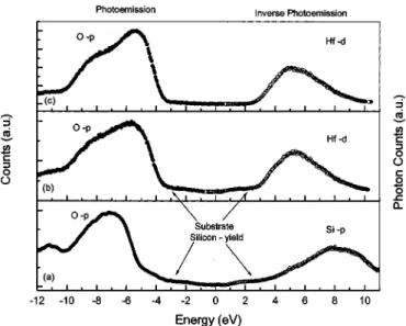
The photoemission and inverse photoemission data ob-tained from a 28 Å HfO2/ SiOxNy/ p-Si are shown in Fig. 2.
The valence band mainly consists of O 2p like nonbonding orbitals ofsymmetry while the conduction band is mainly Hf 5d like nonbonding orbitals. All energies are referenced to the Fermi level which is determined by a clean polycrys-talline gold or platinum sample. Special care is taken when determining the spectrometer response functions for both IPES and PES. This is accomplished by modeling the region
in the vicinity of the Fermi level by a step function and a Gaussian function whose width represents the experimental spectrometer response function. In the case of photoemission experiments, the obtained spectrometer response function is cross checked by the width of the Au 4f doublet, which is equal to the combined broadening due to core-hole lifetime and the spectrometer response function. In this case, the core-hole lifetime for the Au 4f7/2 peak is calculated to be
0.32 eV, in accordance with literature values.9,10 The spec-trometer response functions had Gaussian widths of 0.67 and 0.50 eV for photoemission and inverse photoemission ex-periments, respectively.
B. XRD measurements
X-ray diffraction studies were performed on a series of films of different thicknesses (Fig. 3). The thickness range
FIG. 1. Soft x-ray photoemission spectra of valence band region for a 28 Å HfO2/ SiOxNy/ p-Si gate stack.
FIG. 2. Combined photoemission(쎲) and inverse photoemission (䊊); spec-tra of a 28 Å HfO2/ SiOxNy/ p-Si gate stack.
was 125 – 1150 Å, as determined by RBS assuming a density of 9.68 g / cm3 for all samples. All 12 of the significant
dif-fraction peaks for the 1150 Å sample were consistent with monoclinic HfO2.
11
As the thickness is reduced, the crystal-linity of the films decreases, as is evident from the broaden-ing of the diffraction peaks, consistent with a decrease in the average scattering domain. The diffraction peaks for ortho-rhombic HfO2can be differentiated from those of monoclinic
HfO2by d-spacing comparison alone. The absence of
signifi-cant diffraction intensity at the d spacings of maximum in-tensity for the orthorhombic phases (2= 30.4° and 32.1°),11,12 is strong evidence that the orthorhombic phases are not present to any significant degree. We have also re-ported Fourier transform infrared studies on these samples, where we identified the presence of the monoclinic phase through an assignment of IR-active phonon modes.13
C. Methods for determination of band edges
We(X.Z. and D.V.) have recently performed first prin-ciples density functional theory (DFT) calculations on all crystal phases of HfO2; details of these calculations can be
found elsewhere.3 Although the band gap is not calculated exactly in this method, the shapes and densities of state of the occupied and unoccupied bands are thought to be accu-rate. Since the crystal structure of these films was determined to be predominantly monoclinic, only the theoretical density of states for monoclinic HfO2 is considered here. The VBM
and CBM as determined from the “raw” DFT band structure of the monoclinic phase calculation yield an energy gap of
3.76 eV. In order to determine a more accurate gap as well as the VBM and CBM positions, we have employed the fol-lowing procedure which combines experimental and theoret-ical results. First the theorettheoret-ical density of states for mono-clinic HfO2 is convoluted with the appropriate spectrometer
response functions for both PES and IPES spectra. The height of the first main peak below(above) the VBM (CBM) is normalized (such that the experimental and theoretical heights are the same). Then the broadened theoretical curves in the band edge region are shifted until they align with the experimental curves. The energy shifts needed to align the experimental (PES and IPES) and theoretical densities of states are added to the theoretical gap to obtain a new effec-tive band gap of 6.70 eV. The energy separation (⌬ECBM
= ECBM− Efand⌬EVBM= EVBM− Ef) between the Fermi level
and the VBM and CBM are found to be 3.87 and 2.83 eV, respectively.
If, on the other hand, we were to use the conventional method of linear extrapolation of the experimental valence and conduction band edges to the background intensity level, we would obtain a value of 5.86 eV for the band gap and 3.54 and 2.32 eV for the⌬ECBMand⌬EVBMvalues,
respec-tively. The difference in these two sets of numbers show that the methodology of VBM and CBM assignment is a greater source of uncertainty in Egapand barrier height determination than the experimental result itself. It is also important to note that photoemission and inverse photoemission give a one particle energy gap that, although wider than the convention-ally reported optical gap(which usually involves an exciton), may be more relevant to understanding tunneling through a dielectric. Other methods of gap and edge determination such as UV/Vis spectroscopy, x-ray photoemission spectros-copy(XPS) with shake-up spectral analysis, near-edge x-ray absorption spectroscopy (XAS), should include the exciton gap which may be as high as 1 – 2 eV in some oxides.
D. Determination of band offsets
Figure 4(a) shows the theoretical density of states of the valence and conduction bands for this system. In Fig. 4(b), the theoretical density of states is convoluted with the instru-mental response function, and is plotted along with the ex-perimental measurement of valence and conduction bands. Good agreement is observed between the experimental and theoretical valence band densities of states (specifically the band widths and main features), even though the theoretical density of states is not modified for photoemission cross sec-tions (transition matrix elements). However one would ex-pect that the photoelectron cross section across the band would be similar(if not the same) since the valence band is almost exclusively made up of oxygen 2p-like orbitals of andsymmetries. In the case of the unoccupied conduction band, the overall width of the band and the first two features agree reasonably well with theory. However the intensity in the higher energy region of the conduction band clearly does not agree well.
In order to extract the valence and conduction band off-sets, a knowledge of the position of the Fermi level within the silicon band gap is required. The substrate used was
FIG. 3. X-ray diffraction data for four different HfO2layer thicknesses: 125,
p-type Si with a doping concentration of 1⫻1015cm−3. The
position of the Fermi level with respect to the CBM and VBM of Si can be calculated using standard methods.14,15To obtain the 共Si-HfO2兲 offsets, the energy separation between
the Fermi level and CBM of Si is subtracted from the posi-tion of the CBM of HfO2 with respect to the Fermi level (using our combined experimental-theoretical method).
Fig-ure 5 shows a simplified energy band diagram for this gate stack. The valence and conduction band offsets are then found to be 3.61 and 1.97 eV. These offsets are large enough to confirm HfO2to be a viable high-k candidate from a
bar-rier height perspective. However in order to be able to com-pare the values with results found by others, one must re-member to specify the phase of the HfO2 as well as the
method of edge or gap determination. An additional property of the dielectric material, the electron affinity(EA), can also be determined. Since both the electron affinity of silicon
共4.15 eV兲 and the conduction band offset are known, the
electron affinity of HfO2 can be extracted as 2.18 eV(Table
I). If the straight-line method is used to determine the offset, we obtained 3.28 and 1.46 eV for the valence and conduc-tion band offsets respectively. Another useful result is that the energy separation between the Hf 4f7/2and the VBM are
determined. The energy separation between a given core level(the 4f7/2can be treated essentially as a core here as it
is not involved in bonding) and the VBM is constant for a given material; both shift in essentially an equivalent manner as one changes the chemical environment or local field. Thus even in the absence of valence band measurements, by mea-suring the binding energy of this level, one can easily locate the VBM for a given HfO2 system. The energy separation between the two is 共⌬E Hf 4f7/2– VBM兲 is 13.78 eV (see Fig. 1). Experimentally determined values are summarized in Table I.
Figure 6(a) shows PES and IPES spectra of the substrate SiOxNy/ p-Si, and as well as 10 Å and 28 Å HfO2 films
[Figs. 6(b) and 6(c)]. The substrate silicon yield is visible
through the thinner HfO2 films. The positions of the VBM
and CBM are the same as are observed in the thicker film case, hence the band gap is equal to that of the thicker sample. This set of data, along with similar measurements performed on thicker HfO2 samples, indicate that bulk
be-havior is reached within the first few(3–4) monolayers of the oxide.
E. Band bending in silicon
The photoemission spectra of the Si 2p region before and after deposition, as well as following a forming gas
an-FIG. 4.(a) Theoretical valence band density of states (DOS) for monoclinic HfO2,(b) photoemission spectra of HfO2thin film along with convoluted
DOS,(c) theoretical conduction band DOS for monoclinic HfO2, and(d)
inverse photoemission spectra of HfO2 thin film along with convoluted
DOS.
FIG. 5. Simplified energy band diagram of HfO2/ SiOxNy/ n-Si gate stack (a) intrinsic (b) including band-tail states.
TABLE I. The extracted values for band gap Eg, electron affinity EA,
con-duction band offset CBO, valence band offset VBO, and the energy separa-tion between Hf 4f7/2 photelectron line and valence band maximum 关⌬E 共Hf4f7/2– VBM兲兴. Experiment/theory is determined by assuming
per-fect crystallinity while the efper-fective values are extracted by including the band tail states(at the 2level). All values are in units of eV.
Experimental values Experiment/Theory Effective values Straight-line method Eg 6.70 5.84 5.86 EA 2.18 2.68 2.69 CBO 1.97 1.47 1.46 VBO 3.61 3.25 3.28 ⌬E 共Hf4f7/2– VBM兲 13.78 14.14 14.11
FIG. 6. Combined PES and IPES spectra of(a) 11 Å SiOxNy/ p-Si,(b) 10 Å HfO2/ SiOxNy/ p-Si, and(c) 28 Å HfO2/ SiOxNy/ p-Si.
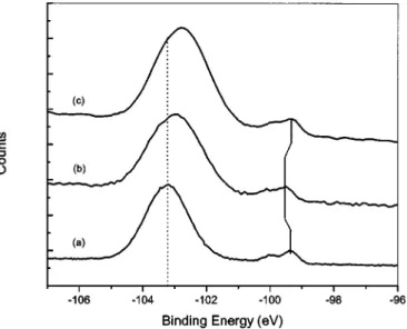
neal(FGA), are shown in Fig. 7. The binding energy of the Siⴰ2p3/2is measured to be 99.30 eV. There is another band
associated with the Si+4 species, which is about 3.91 eV
away from the Siⴰ 2p3/2peak(the curve fitting is not shown,
as it is not trivial). A shift in the unoxidized Si2p3/2peak of
about 0.26 eV towards higher binding energy is observed after deposition, consistent with band bending. An additional feature around⬃3.2 eV on the higher binding energy side of this peak is observed and is tentatively attributed to Si in a
共HfO2兲x共SiO2兲ysilicate, implying a finite level of intermixing
at the HfO2/ SiO2 interface.
F. Comparison of theory and experiment: Band tail states
The theoretical calculations presented in this paper are for bulk oxide crystals of infinite extent. As noted above, due to finite crystallinity of the ultrathin films and the presence of structural and compositional defects, electrical defects may appear. The defects could be charged or neutral, according to their atomic nature, and could in principal exist anywhere(in space and/or energy) in the film. Experimentally, interfacial and/or bulk defect states are observed in a variety of alterna-tive high permittivity materials, some with defect densities on the order of 1013cm−2eV−1 (which translates to a bulk density of 1019cm−3). This value is high enough that these states may contribute to the observed photoemission and in-verse photoemission yield near the band edges. Because of the observed excess density of states near the band edges and the consequence this has on the band edge definition, two values for the offsets as well as the band gap are noted. One solution would be to simply report an average local density of states at each position across the film, and not to define a gap or pair of edges(as preferred by the device community). One way to understand the defect state energies would be to assume a distribution of defect states in the vicinity of the band edges, as the data suggest. If the experimentally deter-mined DOS is taken and subtracted from the theoretical DOS
(following normalization), the difference yields two peaks
close to the two band edges. These two peaks can be mod-eled as a pair of Gaussian curves (Fig. 8) with centrums at −4.01 and 2.83 eV, and widths of 0.58 and 0.59 eV (after subtracting out the corresponding spectrometer response functions outlined above). The literature consensus is that HfO2films have a gap of 5.6– 6.0 eV, although the proof and
methodology of this remains debated.16–20 We obtain this value from our results by defining the edge as the 2level of the Gaussian-modeled band tail states. Although there is no strong theoretical argument to include what we are calling band edge defect states in defining the “real” gap, they may be considered as contributing to an “effective” band gap(see Fig. 8). We also include these effective values in Fig. 5.
Concerning their physical nature, one of the conven-tional assignments of the observed defect states would be to attribute them to band-tail states. The presence of structural disorder can also be caused by(or related to) deviations from ideal stoichiometry(metal vacancies, excess oxygen, oxygen vacancies or impurities such as atomic hydrogen). In fact, these films do contain slightly higher oxygen content than the ideal stoichiometry (at least as measured by MEIS fol-lowing growth) and are also likely to contain excess hydro-gen as deposited. Peacock and Robertson have shown that atomic hydrogen, as an extrinsic defect, would introduce shallow unoccupied states in the vicinity of the conduction band which behave as acceptors.21Foster et al. reported on the vacancy and interstitial defects in HfO2where it is
theo-retically shown that the O2− species would introduce defect states in the vicinity of the valence band. These states are neutral when occupied, and act as donors.22
Kerber et al. reported on conventional charge pumping results on a HfO2/ SiO2/ Si dual-layer gate stack.
23
The charge measured with an amplitude sweep, along with the observation of a strong dependence on charging/decharging time, supported the proposition that defects were located deeper inside the gate stack. All the observed features in the experimental data could be explained qualitatively if defects
FIG. 7. SXPS spectra of Si 2p region of(a) SiOxNy/ p-Si,(b) as-deposited HfO2/ SiOxNy/ p-Si, and(c) HfO2/ SiOxNy/ p-Si after FGA.
FIG. 8. (a) Densities of states of monoclinic HfO2as determined by PES
and IPES, the Gaussian peaks roughly model the presence of occupied and unoccupied band-tail/defect states in the vicinity of the VBM and CBM.(b)
The fit between theoretical and experimental DOS improves after the band tail states subtracted from the measured DOS.
were located in a HfO2layer distributed in energy and space.
It was also argued that the defect states are above the silicon conduction band minimum whose origin was attributed to oxygen vacancies and/or impurities in HfO2. The energy of the states observed in our work(in the vicinity of the HfO2 conduction band minimum) is qualitatively consistent with those proposed by Kerber et al.
G. Electrostatic potential across the gate stack
The charge neutrality level(CNL) of semiconductor sur-face (interface) states is defined as the energy above which the states are empty for a neutral surface (interface).11 The band alignment between two semiconductors is believed to be controlled in part by charge transfer across the interface which results in the creation of interface dipoles. This dipole modifies the barrier heights given by the electron affinity rule,24 which is basically the difference between the elec-tronegativities screened by a factor which depends on the electronic component of the dielectric constant. In the case of HfO2, the bulk CNL lies above the Fermi level of the
p-doped silicon substrate(in other words the electronegativ-ity of HfO2is smaller than that of the silicon substrate).
18
An equalization of the electrochemical potentials occurs when the materials are brought into contact which creates a dipole at the interface. This interface dipole alters the occupancy of interface states due to the charge transfer from HfO2to
sili-con. This leaves positive charge on the dielectric side of interface, with opposite charge appearing in silicon to screen it. This is consistent with our finding of downwards band bending observed for substrate silicon since the downward bending for a p-type silicon substrate is indicative of the presence of negative charge in the silicon. Furthermore the amount of charge can be calculated from the observed band bending in silicon by plotting the surface potential versus charge curve. The amount of charge, for a band bending of 0.26 eV, is found to be 6⫻1012cm−2, which is in good
agreement with the electrical measurements.23
The energy of the orbitals that carry this positive charge
(that is compensated for by a buildup of negative charge in
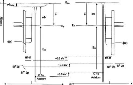
silicon substrate) is of concern. Due to the presence of charges within the gate stack, electrostatic potentials are de-veloped across it. One scenario is depicted in Fig. 9. The
electrostatic potential just outside the surface will be either positive or negative with respect to the potential at infinity, depending on the whether the material’s electrochemicale
potential is smaller or larger than the local work function
.25 In Fig. 9, this is illustrated for a smaller local work function. If one can devise a method to probe this potential just outside the surface, then information regarding local work function will be reached. One such tool is to take ad-vantage of surface hydrocarbons due to atmospheric con-tamination; this is similar to putting inert adatoms (such as Kr, Xe, etc.) on the surface.26,27Although the hydrocarbon species become bound to the surface, they are usually only physisorbed, hence their electronic states are pinned to the local vacuum level(not the Fermi level). One should be care-ful when analyzing such charging, as local fields and polar-ization can shift the relevant states. In our studies, we used thin dielectric films(no thicker than 30 Å) and checked for charging as function of flux and time; no indication of charg-ing is found within the experimental resolution. Our energy reference is the Fermi level obtained by analyzing the va-lence band region of clean polycrystalline inert metal foils
(Au, Pt, Ag, etc.). The Fermi energy observed in this manner
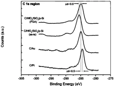
can be used to determine the spectrometer work function. To convert the measured kinetic energies to binding energy, the spectrometer work function should be subtracted from the difference between the excitation energy and the kinetic en-ergy. In this way, the measured binding energies would all be referenced to the same Fermi level. As shown in Fig. 10, the binding energies of the C 1s photoelectron peak from surface hydrocarbons on a Au or Pt surface differ by about⬃0.5 eV which corresponds to the work function difference between Au and Pt(the latter being larger). The p-Si used as substrate has a doping level of 1⫻1015 cm−3 which places the Fermi
level at 0.26 eV above the valence band. Using this informa-tion together with the electron affinity of silicon, one obtains a work function of ⬃5.0 eV for this particular substrate, which is very close to the work function of gold. However, the C 1s position differs from that of Au by about⬃0.6 eV. This indicates a local work function change of ⬃0.6 eV. Following a forming gas anneal, the C 1s positions for both the sample and gold align perfectly, indicating the expected result of equal work functions共⬃5.0 eV兲. Following a
form-FIG. 9. The electrostatic potential distribution across gate stack(a) as-deposited (b) after a forming gas an-neal at 400 ° C.
ing gas anneal (which is known to reduce the number of defects in the gate stack), the Si 2p levels shift by about
⬃0.26 eV whereas the Hf 4f and C 1s levels shift by ⬃0.55 eV. Since any photoelectron originating from layers
above the charge should shift in equal amounts, this leads us to infer that the positive charge is located primarily close to the SiO2/ HfO2 interface. This observed shift is due to the
electrostatic potential across the gate stack, hence the energy band diagram should be corrected for this potential.
IV. CONCLUSION
We have studied the HfO2/ SiOxNy/ p-Si gate stack by
PES and IPES along with first principles calculations. The HfO2 films experimentally examined were predominantly
monoclinic. Combined experimental and theoretical calcula-tions were used to locate the valence band maximum and conduction band minimum. The method used takes into ac-count the spectrometer response function, hence the broad-ening of the spectral features due to limited resolution by excitation source, electronics, etc.
Evidence for the presence of charge in the gate stack is presented, along with a discussion of possible structural and/or compositional origins for the charge defects. The elec-tron affinity of monoclinic HfO2is calculated to be 2.18 eV from the measured band offset and the known electron affin-ity of silicon. The energy separation between the Hf 4f7/2
core level and the VBM is measured and found be 13.85 eV. This energy difference can serve as a valuable input for pho-toemission studies on this material since measuring the bind-ing energy of this core level will enable one to locate the VBM.
Although the presence of defects on spectroscopic and electrical behavior are observed, the origin of the defects could not be unambiguously understood with the presently available data and theory. The presence of band-tail states, as revealed by the comparison of theoretical and experimental results may originate from disorder in the film.
ACKNOWLEDGMENTS
The authors would like to thank the SRC, Sematech, and the NSF for financial support. We also thank J. Robertson, S. Chambers, R. Opila, E. Gusev, T. Gustafsson, and G. Wilk for useful discussions. D. Vanderbilt and X. Zhao acknowl-edge NSF Grant No. DMR-0233925 for financial support.
1
International Technology Roadmap for Semiconductors, Semiconductor Industry Association(2003).
2
G. D. Wilk, R. M. Wallace, and J. M. Anthony, Appl. Phys. Rev. 89,
(2001). 3
X. Zhao and D. Vanderbilt, Phys. Rev. B 65, 075105(2002). 4
X. Zhao and D. Vanderbilt, Mater. Res. Soc. Symp. Proc. 747, 93(2003). 5
D. Redfield, J. P. Wittke, and J. I. Pankove, Phys. Rev. B 2, 1830(1970).
6
C. H. Olk and S. M. Yalisove, Phys. Rev. B 52, 1692(1995).
7
P. Y. Yu and M. Cardona, in Fundamentals of Semiconductors, 3rd ed.
(Springer, Berlin, 2001), pp. 159–202. 8
S. Sayan, S. Aravamudhan, B. W. Busch, W. H. Schulte, F. Cosandey, G. D. Wilk, T. Gustafsson, and E. Garfunkel, J. Vac. Sci. Technol. A 20, 507
(2002). 9
P. H. Citrin and G. K. Wertheim, Phys. Rev. Lett. 41, 1425(1978). 10
E. A. Kraut, R. W. Grant, J. R. Waldrop, and S. P. Kowalczyk, Phys. Rev. B 28, 1965(1983).
11
R. E. Hann, P. R. Suitch, and J. L. Pentecost, J. Am. Ceram. Soc. 68, C285
(1985). 12
O. Ohtaka, T. Yamanaka, and S. Kume, J. Ceram. Soc. Jpn. 99, 826
(1991). 13
M. M. Frank, S. Sayan, S. Dörmann, T. J. Emge, L. S. Wielunski, E. Garfunkel, and Y. J. Chabal, Mater. Sci. Eng., B 109, 6(2004).
14
S. M. Sze, Physics of Semiconductor Devices, 2nd ed.(Wiley, New York,
1981). 15
K. Kano, Semiconductor Devices(Prentice-Hall, Upper Saddle River, NJ, 1998).
16
V. V. Afanas’ev, A. Stesmans, F. Chen, X. Shi, and S. A. Campbell, Appl. Phys. Lett. 81, 1053(2002).
17
A. Callegari, E. Cartier, M. Gribelyuk, H. F. Okorn-Schmidt, and T. Zabel, J. Appl. Phys. 90, 6466(2001).
18
J. Robertson, J. Vac. Sci. Technol. B 18, 1785(2000).
19
J. Robertson, Appl. Surf. Sci. 190, 2(2002). 20
M. Balog, M. Schieber, M. Michman, and S. Patai, Thin Solid Films 41, 247(1977).
21
P. W. Peacock and J. Robertson, Appl. Phys. Lett. 83, 2025(2003).
22
A. S. Foster, F. L. Gejo, A. L. Shluger, and R. M. Nieminen, Phys. Rev. B
65, 174117(2002). 23
A. Kerber et al., IEEE Electron Device Lett. 24, 87(2003). 24
R. L. Anderson, Solid-State Electron. 5, 341(1962).
25
W. F. J. Egelhoff, Surf. Sci. Rep. 6, 213(1986).
26
T. V. W. Janssens, G. R. Castro, and K. Wandelt, Surf. Sci. 399, 15(1998). 27
T. V. W. Janssens, G. R. Castro, K. Wandelt, and J. W. Niemantsverdriet, Phys. Rev. B 49, 14599(1994).
28
S. Sayan, R. A. Bartynski, X. Zhao, E. P. Gusev, D. Vanderbilt M. Croft M. Banaszak-Holl and E. Garfunkel, Phys. Status Solidi B 241, 2246
(2004).
FIG. 10. XPS spectra of the C 1s region of surface hydrocarbon contami-nation on substrates of different work functions.