InGaN/GaN QUANTUM ELECTROABSORPTION
MODULATORS WITH RECORD BREAKING
ELECTROABSORPTION IN BLUE
a thesis
submitted to the department of electrical and
electronics engineering
and the institute of engineering and sciences
of bilkent university
in partial fulfillment of the requirements
for the degree of
master of science
By
Emre SARI
I certify that I have read this thesis and that in my opinion it is fully adequate, in scope and in quality, as a thesis for the degree of Master of Science.
Assist. Prof. Dr. Hilmi Volkan Demir (Supervisor)
I certify that I have read this thesis and that in my opinion it is fully adequate, in scope and in quality, as a thesis for the degree of Master of Science.
Assist. Prof. Dr. Vakur Beh¸cet Ert¨urk
I certify that I have read this thesis and that in my opinion it is fully adequate, in scope and in quality, as a thesis for the degree of Master of Science.
Assist. Prof. Dr. Fatih ¨Omer ˙Ilday
Approved for the Institute of Engineering and Sciences:
Prof. Dr. Mehmet Baray
Director of Institute of Engineering and Sciences
ABSTRACT
InGaN/GaN QUANTUM ELECTROABSORPTION
MODULATORS WITH RECORD BREAKING
ELECTROABSORPTION IN BLUE
Emre SARI
M.S. in Electrical and Electronics Engineering
Supervisor: Assist. Prof. Dr. Hilmi Volkan Demir
June 2007
Silicon based complementary metal-oxide-semiconductor (CMOS) technology has surely moved humankind forward in the information age. Over the years, Si CMOS has also evolved as the necessities of other technologies enabled by CMOS has expanded (for example, as the required speed of operation has in-creased). Consequently, CMOS microelectronics has been continuously replaced by their faster successors thus far. However, there is a physical limit to how fast conventional CMOS chips can run, constrained mainly due to the RC lim-itation of their electrical interconnects. This introduces a bottleneck in operat-ing speed and even downscaloperat-ing interconnects does not solve this problem. As a solution, optical clocking has been proposed and implemented commonly in the near infrared (NIR) where optoelecronic devices are readily available. But, silicon photodetectors fabricated in standard CMOS process unfavorably suffer from diffusion tail problem in NIR, which limits the operating speed, prevent-ing direct high-speed clock injection into Si. To circumvent this problem, one approach is to utilize high-speed III-V photodetectors hybrid integrated on Si chips. This, however, introduces difficulties related to post-CMOS fabrication.
On the other hand, unlike in NIR, optical clock injection directly to Si is possible in the blue, where Si lacks the diffusion tail. However, there exists no chip-scale device particularly implemented to generate and inject optical clock signal blue to date. In this thesis, we propose blue InGaN/GaN based quantum electroab-sorption modulators for a possible chip-scale solution to the modulation of blue clock signal. Here we present the device conception, design, growth, fabrication, experimental characterization, and theoretical analysis of these quantum elec-troabsorption modulators. Growing on polar c-plane of its wurtzite crystal, we obtain InGaN/GaN quantum structures with zig-zag potential profile due to al-ternating polarization-induced electrostatic fields and show that their absorption edge blue-shifts with applied electric field, unlike the red shift of conventional quantum confined Stark effect. In such InGaN/GaN quantum structures, we demonstrate the largest electroabsorption change of 6000 cm−1 (corresponding
to 50 cm−1 absorption coefficient change for 1 V /µm field swing) around 424 nm
ever reported for blue. This implies that the reversed quantum confined Stark effect in these InGaN/GaN quantum zigzag structures in the blue is comparable to the traditional quantum confined Stark effect in the InGaAsP/InP quantum well structures in NIR commercially used in communications. These proof-of-concept demonstrations show that blue InGaN/GaN quantum electroabsorption holds great promise for high-speed optical clock generation and injection directly into Si CMOS chips in the blue.
Keywords: electroabsorption, III-nitrides, modulator, wells, optical clocking.
¨
OZET
MAV˙I DALGABOYU ARALI ˘
GINDA ELEKTROSO ˘
GRULMA
REKORU KIRAN InGaN/GaN KUVANTUM
ELEKTROSO ˘
GRULMA K˙IPLEY˙IC˙ILER˙I
Emre SARI
Elektrik ve Elektronik M¨uhendisli¯gi B¨ol¨um¨u Y¨uksek Lisans
Tez Y¨oneticisi: Yrd. Do¸c. Dr. Hilmi Volkan Demir
Haziran 2007
Hi¸c ¸s¨uphesiz ki silisyum (Si) tabanlı t¨umleyici metal-oksit-yarıiletken (CMOS) teknolojisi ya¸samakta oldu˘gumuz ileti¸sim ¸ca˘gında insano˘glunu ileriye ta¸sıyan teknolojilerdendir. Yıllar ge¸ctik¸ce Si CMOS da kullanıma a¸ctı˘gı teknolojilerin gereksinimlerinin (¨orne˘gin, gereken ¸calı¸sma hızının) artmasıyla evrimle¸sti. Sonu¸c olarak CMOS mikroelektronik devreleri yerlerini daha hızlı varislerine bıraktı. Ancak, geleneksel CMOS yongalarının ¸calı¸sma hızında temel bir fiziksel ¨ust sınır vardır ve bu sınırın ba¸slıca nedeni elektriksel araba˘glantıların RC sınırlamasıdır. Bu ¸calı¸sma hızında bir darbo˘gaza yol a¸cmakta olup araba˘glantıların ¨ol¸cekli k¨u¸c¨ult¨ulmesiyle bile bu darbo˘gaz a¸sılamamaktadır. Bir ¸c¨oz¨um olarak, optik sa-atle denetim ¨onerilmi¸s ve yaygın olarak optoelektronik aygıtların mevcut oldu˘gu yakın kızıl¨otesinde uygulanmı¸stır. Fakat silisyum tabanlı, ¨orne˘gin standart CMOS teknolojisi ile ¨uretilen, fotodetekt¨orler yakın kızıl¨otesinde istenmeyen bir ¸sekilde dif¨uzyon kuyru˘gu sorunu ya¸samaktadır; bu da ¸calı¸sma hızını d¨u¸s¨ur¨up CMOS devrelere do˘grudan optik saat denetimini engellemektedir. Bu sorunu
v
a¸smak i¸cin ¨onerilen ¸c¨oz¨umlerden biri, y¨uksek hızlı III-V fotodetekt¨orleri sil-isyum yongalara melezle¸stirmektir. Ancak bu, CMOS-sonrası fabrikasyon gerek-tirmekte olup yonga ¨uretimini zorla¸stırmaktadır. Di˘ger yandan yakın kızıl¨otesi yerine mavide optik saat denetim sinyalini ¨uretmek ve silisyuma dif¨uzyon prob-lemi olmaksızın do˘grudan sa˘glamak m¨umk¨und¨ur. Ancak ¸su ana kadar mavi dal-gaboyu aralı˘gında optik saat denetim sinyalinin ¨uretilmesi ve silisyuma do˘grudan sa˘glanması i¸cin yonga ¨ol¸cekli bir aygıt yapılmamı¸stır. Bu tezde mavi saat denetim sinyalinin ¨uretimi i¸cin olası bir yonga ¨ol¸cekli aygıt ¸c¨oz¨um¨u olarak In-GaN/GaN tabanlı kuvantum elektroso˘grulma kipleyicilerini sunuyoruz. Burada aygıtlarımızın tasarımı, b¨uy¨ut¨ulmesi, fabrikasyonu, deneysel karakterizasyonu ve kuramsal analizi sunuluyor. Sahip oldu˘gu wurtzite kristal yapısının kutuplu c-d¨uzlemine b¨uy¨utt¨u˘g¨um¨uz InGaN/GaN kuvantum yapılarında kutuplama-sebepli zıt y¨onl¨u elektrostatik alanlarından dolayı zig-zag potansiyel profili g¨ozlemliyoruz ve so˘grulma bant kenarının uygulanan elektrik alanla maviye kaymaya ugradı˘gını deneysel ve teorik olarak g¨osteriyoruz. InGaN/GaN kuvantum yapılarında en y¨uksek 6000 cm−1lik bir so˘grulma katsayısı degi¸simi (1 V/µm elektrik alan
de˘gi¸simine kar¸sılık 50 cm−1 so˘grulma sabiti de˘gi¸simi) elde etmekteyiz. Bu,
g¨ozlemledi˘gimiz tersine kuvantum sınırlamalı Stark etkisinin ileti¸sim sekt¨or¨unde ticari olarak kullanılan ve yakın kızıl¨otesinde ¸calı¸san InGaAsP/InP tabanlı ku-vantum kuyu yapılarındaki geleneksel kuku-vantum sınırlamalı Stark etkisi kadar g¨u¸cl¨u oldu˘gunu g¨ostermektedir. Yapılabilirli˘gini g¨osterdi˘gimiz mavi InGaN/GaN kuvantum elektroso˘grulma kipleyicileri mavi dalgaboyu aralı˘gında y¨uksek hızlı saat denetim sinyalinin ¨uretimi ve silisyum tabanlı CMOS yongalara do˘grudan sa˘glanması i¸cin ¨umit vadetmektedir.
Anahtar Kelimeler: elektroso˘grulma, III-nitr¨urler, kipleyici, kuyular, optik saat denetimi
ACKNOWLEDGMENTS
First, I would like to express my gratitude to my supervisor Prof. Hilmi Volkan Demir for his endless support (in all aspects), guidance and motivation. It is an honor and a great experience to be working with him. Also thanks to all other Demir group members.
I would also like to thank Prof. Ekmel Ozbay for initiating Nanotam, a center of excellence and his former and present group members for their help during my growth, fabrication and characterization training.
Thanks to Prof. In-Hwan Lee for his interest to our work. I think we will do a lot more in this collaboration.
I would like to thank Profs. Vakur B. Erturk and F. Omer Ilday for their helpful comments to this thesis.
I’d like to acknowledge TUBITAK for support during my M.S. studies. Finally I would like to express my love to my family for always being there for me.
Contents
1 INTRODUCTION 1 1.1 Problem Statement . . . 1 1.2 Motivation . . . 2 1.2.1 Device Perspective . . . 2 1.2.2 Materials Perspective . . . 3 1.3 Objective . . . 4 1.4 Summary . . . 42 III-NITRIDE SEMICONDUCTOR MATERIAL 6 2.1 Crystal Structure of III-Nitrides . . . 6
2.2 Quantum Heterostructures of III-Nitrides . . . 7
2.3 Growth of III-Nitrides . . . 11 2.3.1 Metal Organic Chemical Vapor Deposition of III-Nitrides . 12
3 PHYSICS of OPTICAL ELECTROABSORPTION 13
CONTENTS vii
3.1 Optical Absorption in Semiconductors . . . 13
3.2 Electroabsorption Mechanisms . . . 16
3.2.1 Franz-Keldysh Effect . . . 16
3.2.2 Quantum Confined Stark Effect . . . 18
3.3 Quantum Electroabsorption Modeling . . . 20
3.3.1 Transfer Matrix Method and Its Implementation . . . 22
3.3.2 Theoretical Demonstration of Quantum Confined Stark Ef-fect Using Transfer Matrix Method . . . 26
4 DEVICE IMPLEMENTATION 28 4.1 Design Work . . . 28 4.1.1 Quantum Design . . . 28 4.1.2 Epitaxial Design . . . 31 4.1.3 Device Design . . . 32 4.2 Experimental Work . . . 33 4.2.1 Growth . . . 33 4.2.2 Material Characterization . . . 34 4.2.3 Fabrication . . . 38 4.2.4 Device Characterization . . . 39
CONTENTS viii
5.1 Conclusions . . . 49 5.2 Future Directions . . . 50
APPENDIX 52
List of Figures
1.1 Absorption spectra and penetration depth of various semiconduc-tors (After Ref. [5]). . . 2 1.2 Electroabsorption modulator device concept (After Ref. [7]). . . . 3 1.3 Absorption band edges of III-nitrides in the optical spectrum [9]. . 4
2.1 Wurtzite crystal of GaN. White atoms can either be Ga or N, depending on the polarity (After Ref. [9]). . . 7 2.2 Electric field intensity (in MV /cm), in an InxAlyGa1−x−yN/GaN
quantum structures same thickness in well and barrier: (a) our results (black line indicates zero field cases) and (b) After Ref. [11] 10 2.3 A representative band diagram of In0.1Ga0.9N/GaN quantum
zig-zag structure we obtained by combining the available material parameters and electric field calculations. . . 11
3.1 Band-to-band absorption in semiconductors (After Ref. [15]). . . . 14 3.2 A p-i-n photodiode under reverse bias and illumination (After
Ref. [16]). . . 14 3.3 Basic concept of Franz-Keldysh effect (After Ref. [14]) . . . 17
LIST OF FIGURES x
3.4 Basic concept of quantum confined Stark effect. (After Ref. [14]) 19 3.5 Optical absorption spectra for AlGaAs/GaAs quantum well
struc-ture for various electric fields applied perpendicular to quantum well layers measured at room temperature. The spectra are shifted vertically to dashed levels for clarity. (After Ref. [14]) . . . 20 3.6 Implementation of the tunneling resonance method using bisection
method (After Ref. [14]). . . 23 3.7 Associated energy eigenstates for Quantum Structure 1, obtained
by our TMM-based simulation tool. . . 24 3.8 Associated energy eigenstates for quantum structure 2, obtained
by our TMM based simulation tool. . . 25 3.9 Associated electron eigenstates and energy eigenvalues for
Al0.3Ga0.7As/GaAs quantum structure obtained by our TMM
based simulation tool (wavefunctions are normalized to different values for visualization purposes). . . 26 3.10 Absorption spectra for Al0.3Ga0.7As/GaAs quantum structure for
different external electric field intensities obtained by our TMM based simulation tool. . . 27
4.1 Wavefunctions of In0.1Ga0.9N/GaN quantum structures that we
calculate using TMM for zero and non-zero external electric field cases. . . 29 4.2 Absorption spectra for In0.1Ga0.1N/GaN quantum structures that
we calculate using TMM. . . 30 4.3 Layout program view of a modulator in our photomask design. . . 32
LIST OF FIGURES xi
4.4 Layout program view of TLM grids in our photomask design. . . . 32
4.5 In-situ reflectivity measurement results for InGaN/GaN quantum electroabsorption modulator wafer at λ=541.4 nm where the wafer is transparent. . . 34
4.6 0.5 µm × 0.5 µm atomic force microscope image taken from one of our wafers. . . 35
4.7 Photoluminescence spectrum of one of our epi-wafers . . . 36
4.8 A typical wafer transmission spectrum for our InGaN/GaN quan-tum electroabsorption modulators. . . 36
4.9 SIMS analysis results of one of our wafers with 15 InGaN/GaN quantum well/barrier structures. . . 37
4.10 Device after cleaning. . . 38
4.11 Device after mesa etching. . . 38
4.12 Device after p-contact formation. . . 39
4.13 Device after n-contact formation and annealing. . . 39
4.14 Micrograph of a fabricated device. . . 40
4.15 IV curve of one of our modulators, inset shows the semilog scale IV characteristics. . . 40
4.16 Electroluminescence spectrum of one of our modulators. . . 41
4.17 Electroabsorption test setup. . . 42
4.18 Electroabsorption spectra of 4 nm/4 nm InGaN/GaN quantum modulators. Inset shows the 0 V absorption curve separately. . . . 42
LIST OF FIGURES xii
4.19 Absorption coefficient change with respect to 0 V absorption. In-set shows the transmission spectrum for 0 and 5 V reverse bias. . 44 4.20 Field direction dependent demonstration of reversed and
tradi-tional quantum confined Stark effect. E denotes the external elec-tric field and P denotes the polarization-induced electrostatic field inside the quantum well. . . 45 4.21 Electroabsorption spectra of 2.5 nm/7.5 nm InGaN/GaN ield
di-rection dependent experimental demonstration of reversed and traditional quantum confined Stark effect. . . 46 4.22 Absorption coefficient change with respect to 0 V absorption for
the device of 2.5 nm/ 7.5 nm quantum structure. Inset shows the 0 V and 10 V absorption curves separately. . . 46 4.23 Electroabsorption spectra of the device that operates 485 nm for
various reverse bias voltage levels. Inset shows the same of 1 V and 5 V bias in a wider spectrum showing a low level of excitonic effects. . . 47 4.24 Absorption coefficient change with respect to 2 V absorption for
the device optimized for 485 nm wavelength of operation. . . 48
5.1 Dominant mode E-field profile for one of our rib waveguide designs (in collaboration with M. Yorulmaz of our group). . . 50 5.2 Scanning electron micrograph obliquely taken from one of our
de-vices (etched in RIE). . . 51
A.1 Discretization of potential profiles in TMM. . . 52 A.2 Transfer matrix method nomenclature (After Ref. [14]). . . 53
LIST OF FIGURES xiii
List of Tables
2.1 Calculated built-in electrostatic fields for some III-nitride quan-tum structures . . . 9
3.1 Energy eigenvalue results obtained by different methods for Quan-tum Structure 1. . . 24 3.2 Energy eigenvalue results obtained by different methods for
quan-tum structure 2 . . . 25
4.1 A representative epitaxial design. . . 31
Chapter 1
INTRODUCTION
1.1
Problem Statement
Today silicon microelectronics is limited in operating speed. The electrical intercon-nects suffer from the RC limitation1 and scaling does not mitigate this problem [1].
High speed electrical signals (e.g., data or clock) are subject to delays of significant fractions of one clock period and this causes severely limiting electrical effects such as jitter and skew. This leads to a bottleneck in electrical clocking and interconnection. Using optical pulses for these purposes is proposed as a remedy [2].
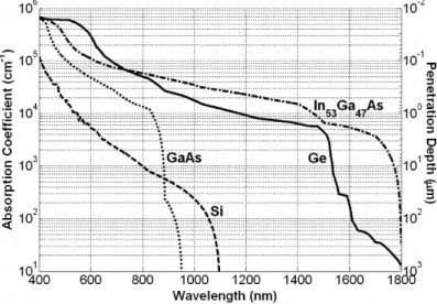
Thus far, optical clock distribution has been commonly implemented in the near in-frared (NIR) spectral region where high performance optoelecronic devices (e.g., in III-arsenide and III-phosphite) are readily available [3]. However, silicon photodetectors, for example, those fabricated in standard complementary metal-oxide-semiconductor (CMOS) process, unfavorably exhibit very low optical absorption (and very long pene-tration depth), as shown in Fig. 1.1 and thus suffer a diffusion tail, with long response time, in this spectral region [4]. This limits the operating speed of Si CMOS pho-todetectors to ∼1 Gbits/s. To circumvent this problem, one approach is to utilize
1e.g., resistance per unit length (for metal lines that carry data and clock signals) increases
with frequency by skin effect.
CHAPTER 1. INTRODUCTION 2
Figure 1.1: Absorption spectra and penetration depth of various semiconductors (After Ref. [5]).
high-speed NIR (e.g., In0.53Ga0.47As) photodetectors hybrid integrated on Si chips. This, however, introduces difficulties related to post-CMOS fabrication.
1.2
Motivation
Unlike in the NIR, optical clock injection directly into Si-based microelectronic circuits via Si-based photodetectors is possible (without violating the CMOS process) by gen-erating optical clock signals in the blue, where Si features a short penetration depth (100 nm at ∼400 nm) as given in Fig. 1.1. Si, in this spectral region, lacks diffusion tail and thus beats the responsivity-speed tradeoff [4]. To date, no chip-scale device implemented to create blue clock signals at high speeds has been reported. Such a device would help to fill the gap between optics and Si-based CMOS electronics and be a feasible solution for CMOS clocking problem.
1.2.1
Device Perspective
For applications that require compactness and high repetition rates (e.g., ∼10 GHz) in optical signal generation, it is customary to use electroabsorption modulators (EAM)
CHAPTER 1. INTRODUCTION 3
Figure 1.2: Electroabsorption modulator device concept (After Ref. [7]).
along with continuous wave (cw) laser diodes. Electroabsorption modulators are de-vices that mix an electrical signal with an optical carrier, the carrier frequency being the optical frequency [6]. A schematic that illustrates the device concept of electroab-sorption modulators is given in Fig. 1.2.
An important figure of merit for EAMs is the contrast ratio (CR), the ratio of optical power level of the binary bit “1” to that of the bit “0”. This figure of merit affects the receiver’s ability to distinguish each bit and thus the bit error rate (BER). Contrast ratio is usually expressed in dB as given in Eq. (1.1). Although a contrast ratio of 3 dB is demonstrated to be sufficient for applications with short distance optical pulse propagation [8], such as in optical clocking and interconnection, , a CR of >10 dB is desirable for system applications.
CR = 10 ¯ ¯ ¯ ¯log10 µ P1 P0 ¶¯¯ ¯ ¯ (1.1)
1.2.2
Materials Perspective
Since the demonstration of the first InGaN /GaN -based blue light emitting diode (LED) in 1993, there has been an enormous technical interest in III-nitride material system. This interest has increased as green to near-ultraviolet LEDs were commer-cialized and the first blue laser diode was demonstrated. Since then, many electronic2
CHAPTER 1. INTRODUCTION 4
Figure 1.3: Absorption band edges of III-nitrides in the optical spectrum [9].
and optoelectronic3 devices and systems4 have been rapidly-successfully demonstrated and many of them were commercialized.
This rapid improvement and interest stem from the unique properties that this material system offers. Since III-nitrides are direct bandgap materials, they are very useful for optoelectronic devices. Also, using their alloys, a very large wavelength region (from ∼200 nm for AlN to longer than 1200 nm for InN ) that includes the whole visible spectrum can be spanned.
1.3
Objective
Our main objective in this thesis is to investigate III-nitride based quantum electroab-sorption modulators as a new chip-scale optoelectronic device for optical clock genera-tion and understand the underlying physics behind them. We also aim at studying the device properties through engineering quantum structures for a stronger electroabsorp-tion effect. We further target at developing a strong know-how in III-nitride device design and implementation.
1.4
Summary
This thesis is organized as follows. In Chapter 2, we review basic material properties of III-nitrides and present a brief overview of their quantum heterostructures and growth.
3e.g., blue laser diodes, white, blue and green LEDs, solar-blind photodetectors 4e.g., BluRay DVD drives, AlGaN/GaN HEMT power amplifiers
CHAPTER 1. INTRODUCTION 5
In Chapter 3, we provide a background on optical electroabsorption by explaining ba-sic electroabsorption mechanisms. In this chapter we also introduce transfer matrix method, a powerful technique that was used in our analysis of quantum heterostruc-tures. In Chapter 4, we present our theoretical and experimental work on the design and implementation of our InGaN/GaN based blue quantum electroabsorption modu-lators. In the last chapter we conclude by summarizing our accomplishments and give an outlook about our future directions.
Chapter 2
III-NITRIDE
SEMICONDUCTOR
MATERIAL
As mentioned in the first chapter, III-nitrides are direct bandgap semiconductors with alloys (InxAlyGa1−x−yN , 0 ≤ x, y, x + y ≤ 1) of bandgap energies spanning a very
wide range of optical spectrum. As a result, not only III-nitride platform serves today’s high-tech industry by its optoelectronic devices demonstrated so far, but it also holds a great promise for new ones. To design and demonstrate new III-nitride devices for their respective applications, it is essential to understand their material properties. This chapter deals primarily with these properties and explains how to engineer them using quantum heterostructures, along with their growth using metal organic chemical vapor deposition technique.
2.1
Crystal Structure of III-Nitrides
Group III-nitrides are found in three different crystal structures being zincblende, rocksalt and wurtzite. Among these, primarily because of the obtained high crystal
CHAPTER 2. III-NITRIDE SEMICONDUCTOR MATERIAL 7
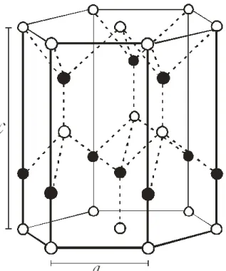
Figure 2.1: Wurtzite crystal of GaN. White atoms can either be Ga or N, de-pending on the polarity (After Ref. [9]).
quality and the relative ease of growth, wurtzite is the dominant one. Wurtzite crystal structure is characterized by the lattice parameters a and c. This configuration, e.g., for GaN consists of alternating biatomic closed-packed (0001) planes of Ga and N pairs stacked in an alternating sequence [9] as shown in Fig. 2.1. Atoms in the first and third layer are symmetrically aligned with each other. As seen in Fig. 2.1, wurtzite structure does not have an inversion plane perpendicular to the c-axis. Thus the surfaces of the crystals grown on c-plane have either a Group III element (Al, Ga or In) polarity or an N polarity. The influence of this polarization will be discussed later in this chapter.
2.2
Quantum Heterostructures of III-Nitrides
Semiconductor heterostructure is formed by two types of interfacing semiconductors (i.e., in heterojunctions) to achieve characteristics that are not feasible in either type of the materials separately. By simply cascading (at least two of) such structures
CHAPTER 2. III-NITRIDE SEMICONDUCTOR MATERIAL 8
very close to each other (about a few nanometers), it is possible to form quantum heterostructures (wells and barriers), which render very interesting quantum effects from a device point of view.
As mentioned earlier, wurtzite III-nitrides have a polarity along their c-axis (i.e., [0001]) and this is the conventional growth axis. Due to low crystal symmetry and deviation of lattice parameters, intrinsic (spontaneous) polarization is observed even in their bulk form. The direction of this polarization field always points from metal atom to N atom [9]. Because of the discontinuity of total polarization, sum of sponta-neous polarization (Psp), and relatively strong strain-induced piezoelectric polarization
(Ppz) fields, built-in sheet charges of very large density are induced in their
hetero-junctions1. The density of these sheet charges (σ) can exceed ±1013cm−2 [10]. In
quantum heterostructures, the same effect is observed as built-in electric fields of huge intensity. Since this is an intrinsic effect, it must cause no potential built up over the whole well-barrier structure and this can be used as a boundary condition in their analysis [11].
From a circuit theory point of view, they form a structure very similar to a series of parallel plate capacitors. Charges on each capacitor plate and the voltage drop on each capacitor alternates in sign and they are equal in absolute value, due to charge neutrality and zero voltage build-up conditions imposed by the circuit.
Spontaneous polarization field, Psp, is known for bulk GaN , AlN and InN . For their alloys, this is estimated by a Vegard-like rule (i.e., linear interpolation) [11]. Strain-induced piezoelectric polarization, Ppz, expression is given as follows [12]:
Ppz = ←→e · −→² (2.1)
where ←→e is the piezoelectric constants tensor and −→² is the strain field of the material, which can both be estimated by the linear interpolation.
CHAPTER 2. III-NITRIDE SEMICONDUCTOR MATERIAL 9
Under the mentioned boundary condition, we obtain the built-in electrostatic field intensities for multiple quantum well structures as follows:
Ewelltot = Ewellsp + Ewellpz = (P
barrier
sp + Pbarrierpz ) − (Pwellsp + Pwellpz )
²well+ dwell
dbarrier²barrier
(2.2) and
Ebarriertot = Ebarriersp + Ebarrierpz = (P
well
sp + Pwellpz ) − (Pbarriersp + Pbarrierpz )
²barrier+ dbarrierdwell ²well
(2.3)
Using these expressions and relevant material parameters available in the litera-ture, we calculate the built-in electrostatic fields in some of polar III-nitride quantum multiple well structures as listed in Table (2.1).
Table 2.1: Calculated built-in electrostatic fields for some III-nitride quantum structures
Well Barrier dwell dbar Ewell Ebar
In0.05Ga0.95N GaN 4 nm 4 nm -88.1 V /µm 88.1 V /µm In0.1Ga0.9N GaN 4 nm 4 nm -175.4 V /µm 175.4 V /µm In0.1Ga0.9N GaN 4 nm 6 nm -209 V /µm 139 V /µm In0.1Ga0.9N GaN 4 nm ∞ -340 V /µm 0+ V /µm GaN Al0.1Ga0.9N 4 nm 6 nm -87.2 V /µm 58 V /µm GaN In0.1Al0.9N 4 nm 6 nm -610.4 V /µm 406.9 V /µm GaN In0.11Al0.287Ga0.603N 4 nm 4 nm 0 V /µm 0 V /µm
As seen in Table (2.1), and intuitively from Eq.s (2.2) and (2.3), the electrostatic field inside the quantum well decreases with the well-to-barrier width ratio (dwell/dbar)
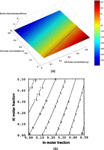
and with the mismatch between well and barrier layers. We have polarization-induced electrostatic fields with lower intensities for AlGaN/GaN quantum structures com-pared to InGaN/GaN quantum structures. Also, in principle, with the appropriate InN and AlN molar concentrations, it is possible to achieve zero built-in electrostatic fields inside both wells and barriers2. When we compare our calculation results of
these built-in electrostatic fields, we observe that they perfectly match with the other theoretical results in the literature as depicted in Fig. 2.2. To produce new devices with quantum structures in III-nitride platform, one has to carefully consider these fields in his design.
CHAPTER 2. III-NITRIDE SEMICONDUCTOR MATERIAL 10
Figure 2.2: Electric field intensity (in MV /cm), in an InxAlyGa1−x−yN/GaN
quantum structures same thickness in well and barrier: (a) our results (black line indicates zero field cases) and (b) After Ref. [11]
CHAPTER 2. III-NITRIDE SEMICONDUCTOR MATERIAL 11
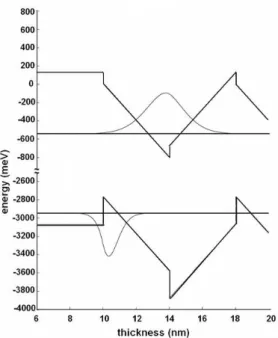
Figure 2.3: A representative band diagram of In0.1Ga0.9N/GaN quantum
zig-zag structure we obtained by combining the available material parameters and electric field calculations.
Additionally, using bandgap energy values of InN, GaN, and AlN, and conduction and valence band offsets for their heterostructures, we obtain the band diagram of any c-plane (polar) III-nitride quantum structure, one of which is depicted in Fig. 2.3 for In0.1Ga0.9N /GaN quantum structure as an example.
2.3
Growth of III-Nitrides
There are several different techniques for the growth of III-Nitrides. Metal organic chemical vapor deposition (MOCVD), molecular beam epitaxy (MBE) and hydride vapor phase epitaxy (HVPE) are the most popular ones amongst all. As a common property of these methods, it is much more convenient and easier to grow c-plane Ga-face GaN . However, and unfortunately, there has been no feasible technique for the synthesis of a native substrate for this material’s growth, at least until now. So, heteroepitaxy is a must for the growth of these materials [9].
CHAPTER 2. III-NITRIDE SEMICONDUCTOR MATERIAL 12
Due to their low lattice mismatch and/or thermal expansion coefficient mismatch to GaN , the most commonly used substrates are sapphire (Al2O3), silicon (Si), and
silicon carbide (SiC) [9]. By growing a thick GaN layer on these substrates in appro-priate conditions, one can get a crystalline GaN , with a reasonably high quality. For all of our devices, we use MOCVD technique and grow the epitaxial structures on the c-plane sapphire and obtain Group III-face crystals.
2.3.1
Metal Organic Chemical Vapor Deposition of
III-Nitrides
MOCVD is the most popular technique of producing GaN based high power light emitting diodes (LEDs) that have been commercially available for about 13 years [13]. The technique is based on the deposition of atoms that are set free by chemical re-actions that occur at high temperatures ranging from 500oC (for InN ) to 1200oC
(for AlN ). These reactions take place between metal organic vapors (group-III mate-rial sources) and hydrides (the nitrogen sources). These substances are called pre-cursors. The precursors commonly used in MOCVD growth of InxAlyGa1−x−yN semiconductors are three-methyl gallium (TMGa or Ga(CH3)3), three-ethyl gallium
(TEGa or Ga(C2H5)3), three-methyl aluminum (TMAl or Al(CH3)3), three-methyl indium (TMIn or In(CH3)3) and ammonia (N H3). For the n- and p-doped growth
of III-nitrides, silane (SiH4) and bis-cyclopentadienylmagnesium (CpM g2) are used, respectively. A representative chemical reaction between the precursors is given in (2.4):
X × In(CH3)3+ (1 − X) × Ga(CH3)3+ N H3→ InxGa1−xN + 3CH4 (2.4)
By intentionally slowing down this reaction and reducing the MOCVD growth rate (to ∼ 1 nm/minute), one can achieve high-quality GaN-based quantum structures in a controlled manner.
Chapter 3
PHYSICS of OPTICAL
ELECTROABSORPTION
This chapter deals primarily with the physics of optical absorption and electroab-sorption in semiconductors. It also introduces two main electroabelectroab-sorption mecha-nisms (Franz-Keldysh and quantum confined Stark effects) and a quantum mechanical method to analyze the quantum electroabsorption.
3.1
Optical Absorption in Semiconductors
In semiconductors, optical absorption is generally referred to as the generation of a photocarrier (electron-hole) pair as response to an incident photon. For the case of most semiconductor structures and photon energies, this carrier generation usually occurs between the conduction band and the valence band as depicted in Fig. 3.1. The likelihood of this event is proportional to the probability of finding an electron in the conduction band and a hole in the valence band in the same vicinity [14].
For indirect bandgap semiconductors, this process must usually be assisted by phonon emission to conserve momentum during this process, whereas for direct
CHAPTER 3. PHYSICS OF OPTICAL ELECTROABSORPTION 14
Figure 3.1: Band-to-band absorption in semiconductors (After Ref. [15]).
Figure 3.2: A p-i-n photodiode under reverse bias and illumination (After Ref. [16]).
bandgap semiconductors phonons are not involved in the optical transition. Pho-todiodes (e.g., photodetectors and electroabsorption modulators) are usually operated at reverse bias voltages. Generated photocarrier pairs are collected through the drift process and they contribute to reverse bias current as illustrated in Fig. 3.2.
There are a number of definitions that help us examine the properties and perfor-mance of such devices in this context. The first definition is the quantum efficiency, η, which is the probability that a single photon, incident on the device, generates an electron-hole pair that contributes to the photodiode current (i.e., photocurrent). In a statistical point of view, η is the ratio of the flux of generated electron-hole pairs
CHAPTER 3. PHYSICS OF OPTICAL ELECTROABSORPTION 15
that contribute to the photocurrent (Φe) to the flux of photons incident on the device
(Φp) [15]. The generic expression of quantum efficiency is given as:
Φe
Φp , η = (1 − R)ζ(1 − e
−αd) (3.1)
The first factor, (1-R), in the right hand side of this expression represents the ratio of photons that make it into the device (i.e., transmission coefficient), in other words the ones that survive through Fresnel reflection, R. The second factor, ζ, represents the ratio of electron-hole pairs that successfully contribute to photocurrent. And the third factor represents the fraction of photon flux absorbed in the active (absorbing) region of the device, coming from the model that formally explains this process as an exponential attenuation with the defined absorption constant, α [15].
Another definition for such devices is the responsivity <, which is the ratio of photocurrent, ip, to the incident optical power, Po. By using the expressions of optical
power and photocurrent relating to photon and electron flux, respectively, we arrive at the following expression for < that relates to η:
< = ip Po = ηe hν = η λ 1.24 (3.2)
where λ is the wavelength given in µm and < is given in A/W.
By combining Eq.s (3.1) and (3.2) and assuming a constant Fresnel reflection co-efficient, R, and a constant ζ over a spectrum, we arrive at the following compact formula that spectrally relates ip and Po to α for a certain structure having an active
layer thickness of d: α = −1 dln µ 1 − ip Poλ 1.24 ζ(1 − R) ¶ (3.3)
As mentioned earlier, these definitions are very helpful for examining the device performance and for understanding the physics of such devices, especially electroab-sorption modulators.
CHAPTER 3. PHYSICS OF OPTICAL ELECTROABSORPTION 16
3.2
Electroabsorption Mechanisms
Electroabsorption is the phenomenon where absorption characteristics of a material changes in response to an externally applied electric field, E. This phenomenon is usu-ally utilized by a few mechanisms in semiconductors. These mechanisms are interesting and important for practical purposes because they enable optoelectronic modulators, which are the key elements in optical communications.
Electroabsorption mechanisms merely require an electric field to be applied across a semiconductor and this is usually achieved within a reverse biased diode structure. Their operating speed is generally limited by RC time constants of themselves (due to parasitic resistance and device capacitance) since neither population inversion nor carrier injection is required for these effects to take place. So the speed issues are not affected by the time constants associated with carrier population changes and hence it is possible to utilize them for high speed operation by good device engineering.
3.2.1
Franz-Keldysh Effect
As the first of such mechanisms, we start investigating Franz-Keldysh effect (FKE). The Franz-Keldysh effect is observed in bulk semiconductors where conduction and valence bands can be viewed as to be tilted when an external electric field is applied. By the application of the electric field, electrons and holes can tunnel into conduction and valence bands, respectively [14]. Photons having slightly less energy than the bandgap energy, Eg, of the semiconductor can be absorbed by this tunneling - whereas this cannot be the case when no electric field is applied and excitonic effects (i.e., Coulomb interaction between electron and holes) are neglected. The basic mechanism of FKE is depicted in Fig. 3.3.
It is possible to notice from the visual description of FKE that the probability of finding an excess electron and hole in the same vicinity (quantitatively, absolute
CHAPTER 3. PHYSICS OF OPTICAL ELECTROABSORPTION 17
Figure 3.3: Basic concept of Franz-Keldysh effect (After Ref. [14])
squared-overlap integral of normalized electron and hole wavefunctions), which is pro-portional to the absorption level, is much less than 1 for any case. Hence, the depen-dence of absorption coefficient on the E-field intensity is very low. It is also apparent that absorption edge, the longest wavelength at which absorption occurs, shifts to longer wavelengths (i.e., redshifts) when electric field is applied regardless of the direc-tion of the E-field.
As mentioned earlier, when light propagates through the semiconductor its inten-sity decays exponentially with a “length constant” of 1/α. α is the absorption constant and is a function of photon energy (i.e., wavelength), and now E field. However, as qualitatively explained, it is not a strong function of electric field for bulk semiconduc-tors. As a typical value, ∼2 cm−1 of absorption coefficient change is achievable by an
electric field change of 1 V/µm in the transparent region of GaN [17].
From a device point of view, for a good electroabsorption modulator operation, it is essential to have a large absorption coefficient change with a moderate level of voltage swing across the device. The FKE can give considerably good device operation in terms of contrast ratio when waveguide architecture is utilized, where optical interaction with the active medium is increased. But in lumped RC operation, these devices are usually beaten by speed issues due to requirements of high voltage change and long waveguides, latter being related to parasitic device capacitance, (unless used in distributed RC operation [e.g., traveling wave modulators]).
CHAPTER 3. PHYSICS OF OPTICAL ELECTROABSORPTION 18
As a confirmation of this conclusion, experimental studies and theoretical analysis available in the literature (even the ones that take excitonic effects into account) show that it is not easy to have a large contrast ratio for very high speeds using a bulk electroabsorption modulator utilizing FKE. There has been a moderate number of modulators reported utilizing FKE that operate in near infrared [18] and near UV range [19].
3.2.2
Quantum Confined Stark Effect
Another and much stronger electroabsorption mechanism in semiconductors is the quantum-confined Stark effect (QCSE), which is the quantized version of FKE.
Quantum heterostructures (wells, wires and dots), having confined dimension(s) of the order of one Bohr exciton radius (a few nanometers), exhibit very strong exci-tonic properties such as strong photoluminescence (PL) peaks at room temperature, and sharp absorption edges [14]. Theoretical and experimental studies have shown that these structures possess strong electroabsorption properties when electric field is applied perpendicular to the confined dimension(s). Similar to FKE, absorption edge shifts to longer wavelengths (i.e., redshifts) as the applied E field is increased [14]. This mechanism is depicted for a GaAs-like (in terms of electron and hole effective masses) infinite quantum well in Fig. 3.4.
There are a couple of remarks to note in the visual description of QCSE. First, electron and hole are pulled in opposite directions by the E field and electron and hole wavefunctions at first energy states overlap relatively less for E 6= 0 case. Second, pre-viously forbidden-like transitions are allowed with the application of E field, in other words electron and hole wavefunctions at other energy states are not orthogonal any-more. Also, absolute-squared overlap integral of normalized non-orthogonal electron and hole wavefunctions for E 6= 0 case is close to 1, but not as large as E = 0 case - in agreement with the sum rules of quantum mechanics [20]. Also, the transition energy between electron and hole ground states, he1|E|h1i, is smaller than that of no-field case, giving rise to the redshift of the absorption edge [20].
CHAPTER 3. PHYSICS OF OPTICAL ELECTROABSORPTION 19
Figure 3.4: Basic concept of quantum confined Stark effect. (After Ref. [14])
A representative measured absorption spectrum for GaAs/AlGaAs multiple quan-tum well (MQW) structure under different external electric field strengths perpendic-ular to the quantum wells is given in Fig 3.5 [14].
As seen in Fig. 3.5, excitonic peak can clearly be observed for low electric field intensity values, since quantum confinement keeps electron and hole close to each other. This property makes QCSE much more useful for electroabsorption modulation purposes compared to FKE.
QCSE has been widely studied and engineered for related applications in GaAs and InP platform. Many commercially available high speed quantum electroabsorption modulators, operating in the near infrared (NIR) region that have been widely used in optical telecommunication links [7] and recently demonstrated advanced optoelectronic devices such as wavelength converting crossbar switches [21] utilize QCSE.
CHAPTER 3. PHYSICS OF OPTICAL ELECTROABSORPTION 20
Figure 3.5: Optical absorption spectra for AlGaAs/GaAs quantum well structure for various electric fields applied perpendicular to quantum well layers measured at room temperature. The spectra are shifted vertically to dashed levels for clarity. (After Ref. [14])
3.3
Quantum Electroabsorption Modeling
The electroabsorption performance of quantum structures can be analyzed independent of the architecture and electric field application mechanism of the device. Since these quantum structures are very important in the performance of the modulators, it is essential to analyze quantum structure candidates in the design of these devices.
Any quantum structure of finite or infinite quantum well problem can be solved exactly, but only for zero E field case. Because of this, it is not a preferred way to solve problems analytically when designing EAMs. Instead, numerical methods are used for this purpose. But it is helpful to verify the reliability of a proposed or implemented numerical method, by comparing with the exact solution in simple problems.
There is a number of numerical methods developed to design quantum EAMs of arbitrary potential profiles. Some of these methods are the finite element method (FEM), finite difference method (FDM), Fourier transform method (FTM), and the transfer matrix method (TMM).
These methods are based on the solution of time independent Schr¨odinger equation (TISE) for the electron (in conduction band) and the hole (in valence band) for semi-conductor structures of known material properties. For our purposes TISE excellently
CHAPTER 3. PHYSICS OF OPTICAL ELECTROABSORPTION 21
describes electron and hole energy eigenstates [14]1. Time independent Schr¨odinger
equation is an eigenvalue problem and its solution describes the energy state of carri-ers for the corresponding potential profile.
Time independent Schr¨odinger equation for the electron in a quantum well and barrier structure under the electric field E in z-direction can be expressed as2:
· − ~ 2 2me ∂2 ∂z2 e + Ve(ze) − eE · ˆze ¸ φe(ze) = Encφe(ze) (3.4)
Here, in Eq. (3.4), Ve is described by the conduction band potential profile of the
quantum structure, me is the electron effective mass, φeis the complex electron
wave-function and Enc is the energy eigenvalue of electron in the reference frame described
by Ve.
It is straightforward to write and understand the same equation for holes just by interchanging associated electron terms (coordinate, effective mass, potential and charge) with hole terms as in Eq. (3.5):
· − ~ 2 2mh ∂2 ∂z2 h + Vh(zh) − eE · ˆzh ¸ φh(zh) = Envφe(zh) (3.5)
The resultant electron and hole wavefunctions have discrete energy eigenvalues due to the quantum mechanical essence of the system. By taking the absolute-squared overlap integral of complex electron and hole wavefunctions along the z-axis, one can get a value proportional to probability of finding an electron and a hole in the same vicinity with an energy difference of Eg+Env+Enc. This energy is called the transition energy between particular electron and hole states. This information is very useful in predicting the spectral electroabsorption behavior of the analyzed quantum structure. Because, each transition that has an energy smaller than particular photon energy adds to absorption rate of such photons by an amount proportional to absolute-squared overlap integral of corresponding electron and hole states.
1Because electroabsorption mechanisms are much faster (∼0.1 ps) than the rise/fall time of
devices (∼10 ps).
CHAPTER 3. PHYSICS OF OPTICAL ELECTROABSORPTION 22
Although this way of solving electron and hole energy eigenvalue problem does not take excitonic effects into account by itself, it gives a strong idea about device perfor-mance. Also, excitonic effects are introduced as a broadening and a slight redshift of the absorption edge3 according to the value of the overlap integral as long as the
exci-tons are not ionized by internal or external electric fields. For our prospective quantum EAMs, we developed an in-house simulation tool implementing transfer matrix method to be used in our design phase.
3.3.1
Transfer Matrix Method and Its Implementation
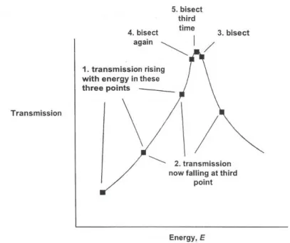
Transfer matrix method (TMM), like other methods for the numerical analysis of arbi-trary (especially, quantum-confined) structures, formally approximates energy eigen-values and eigenstates of the structure in question. In the analysis of such an arbitrary potential structure - changing in one direction - we represent it by a step-wise approx-imation. This reduces the problem of an arbitrary potential to that of a set of many constant potentials obeying appropriate boundary conditions. In such a simple con-stant potential, the wave is either sinusoidal or exponential. In the formalism of TMM, each of these layers of constant potential have a certain transmission matrix as a func-tion of energy [14], like the ABCD matrix in the analysis of optical components and of two-port electromagnetic networks. For an electron (or hole) having some particular energy, its intensity transmission can be found just by multiplication of these matrices, i.e., cascading each of these layers. For each quasi − eigenstate4, this probability has
a local maxima - in other words, it is resonant with the potential profile.
As depicted in Fig. 3.6, starting with an hypothetical wave (with some particular energy) impinging on one side of the structure, using any maxima finding algorithm (e.g., bisection method), one can iteratively find the quasi−eigenvalue along with its associated quasi−eigenstate. This way of searching eigenstates is called the tunneling resonance method (TRM). The transfer matrix method formalism and the tunneling resonance method are elaborately explained in Appendix A.
3Since Coulomb interaction enhances electron-hole pair generation 4not “the eigenstate” due to the numerical nature of the analysis
CHAPTER 3. PHYSICS OF OPTICAL ELECTROABSORPTION 23
Figure 3.6: Implementation of the tunneling resonance method using bisection method (After Ref. [14]).
We developed and used our simulation tool implementing TMM in a MATLABr installed personal computer (PC) environment.
We started using our in-house simulation tool by checking the reliability of TMM and our implementation. For this, we compared our first simulation results with the results obtained by implementation of other numerical methods and exact solutions for two exactly solvable quantum mechanics problems available in the literature.
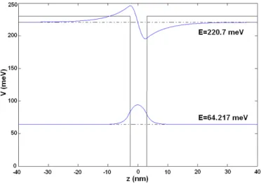
Quantum Structure 1
As the first comparison we simulated a single quantum well structure with a barrier height (Vba) of 230 meV and a well width (Lw) of 56 ˚A. Particle effective mass for the well (mw) was 0.067m0 and for the barrier (mb) it was 0.0919m0, where m0 is
the electron rest mass. For this problem, exact solution gives two bound states with energy eigenvalues of 64.2 and 220.7 meV from the bottom of the well.
For this problem, our and other available results for energy eigenvalues are sum-marized in Table (3.1). Almost all of the results, including our results, match with the
CHAPTER 3. PHYSICS OF OPTICAL ELECTROABSORPTION 24
Figure 3.7: Associated energy eigenstates for Quantum Structure 1, obtained by our TMM-based simulation tool.
exact solution (finite difference methof [FDM] After Ref. [22] and Fourier transform method [FTM] courtesy of H. V. Demir). Fig. 3.7 shows associated eigenstates and
Table 3.1: Energy eigenvalue results obtained by different methods for Quantum Structure 1. Energy states E1(meV) E2 (meV) Exact 64.2 220.7 FDM 64.3 220.7 FTM 64.2 220.7 TMM 64.217 220.7
their wavefunctions obtained by our simulation tool.
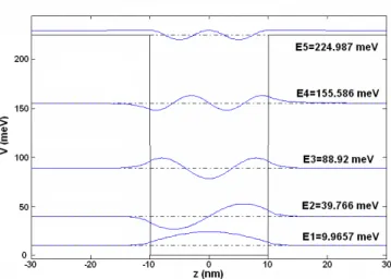
Quantum Structure 2
It is usually challenging to find loosely-bound states for all of numerical techniques in the analysis of quantum-confined structures. To reach the conclusion that our tool works also for loosely bound states, we examined a single quantum well structure with a barrier height (Vba) of 225 meV and a well width (Lw) of 200 ˚A - for which,
exact solution predicts a loosely bound state. Particle effective mass for the well (mw) was 0.067m0 and for the barrier (mb) it was 0.0919m0, where, again, m0 is the
CHAPTER 3. PHYSICS OF OPTICAL ELECTROABSORPTION 25
Figure 3.8: Associated energy eigenstates for quantum structure 2, obtained by our TMM based simulation tool.
being a loosely-bound one. The results are summarized in Table (3.2) (finite element method [FEM] After Ref. [23], and Fourier transform method [FTM], courtesy of H.V. Demir). Fig. 3.8 shows associated eigenstates (including the loosely bound state)
Table 3.2: Energy eigenvalue results obtained by different methods for quantum structure 2
Energy states
E1(meV) E2(meV) E3(meV) E4(meV) E5(meV)
Exact 9.97 39.77 88.92 155.58 224.99
FEM 9.97 39.77 88.93 155.59 Not Found
FTM 9.97 39.77 88.92 155.57 224.9
TMM 9.9657 39.766 88.92 155.586 224.987
and their wavefunctions obtained by our simulation tool. Our results showed that our TMM-based simulation tool successfully works and that we can use it in the design and analysis of any arbitrary potential profile (including those made of GaN based material system).
CHAPTER 3. PHYSICS OF OPTICAL ELECTROABSORPTION 26
Figure 3.9: Associated electron eigenstates and energy eigenvalues for Al0.3Ga0.7As/GaAs quantum structure obtained by our TMM based simulation
tool (wavefunctions are normalized to different values for visualization purposes).
3.3.2
Theoretical Demonstration of Quantum Confined
Stark Effect Using Transfer Matrix Method
Using our simulation tool, we can also demonstrate quantum confined Stark effect. We computed the electron and hole states of a GaAs/Al0.3Ga0.7As single quantum well
structure for different external electric field intensity levels. For the electron states we obtained the wavefunction and energy eigenvalues as summarized in Fig. 3.9 (here note that no broadening is used). As depicted in this figure, the energy eigenvalue of the electron decreases and electron wavefunction moves under the effect of the external field as the field is increased. In agreement with the QCSE mechanism.
The resulting absorption spectrum we obtained is shown in Fig. 3.10. This figure shows that we can successfully demonstrate QCSE with its redshift with increasing electric field in our simulation environment and model quantum electroabsorption in semiconductor quantum structures.
CHAPTER 3. PHYSICS OF OPTICAL ELECTROABSORPTION 27
Figure 3.10: Absorption spectra for Al0.3Ga0.7As/GaAs quantum structure for
different external electric field intensities obtained by our TMM based simulation tool.
Chapter 4
DEVICE IMPLEMENTATION
This chapter summarizes our main device implementation on III-nitride device plat-form, describing our design approach, material growth, device fabrication, and char-acterization step by step.
4.1
Design Work
Our design work consists of three parts: Quantum design in which we design the quantum structures, the epitaxial design in which we design the set of epitaxial layers according to the quantum design and device consideration and finally the device design in which we design the architecture of our devices.
4.1.1
Quantum Design
In our quantum design part, we basically simulate possible quantum structures for their utilization in electroabsorption. We compute the electron and hole energy eigen-values and wavefunctions using TMM based simulation tool with appropriate material parameters. We then calculate their absolute-squared overlap integrals for different levels of external electric fields as we did for AlGaAs/GaAs quantum structures. For
CHAPTER 4. DEVICE IMPLEMENTATION 29
Figure 4.1: Wavefunctions of In0.1Ga0.9N/GaN quantum structures that we
calculate using TMM for zero and non-zero external electric field cases.
a desired wavelength of operation (e.g., 400 nm) we obtain the predicted absorption spectra and so the change in absorption level with the external electric field.
As a quantum structure to be examined, we can simulate an In0.1Ga0.9N/GaN multiple quantum well structure that consists of 5 quantum wells and barriers each being 4 nm thick. The band diagrams for zero and non-zero external field cases and the electron and hole wavefunctions we computed according to them are shown in Fig. 4.1.
In Fig. 4.1 we theoretically show that absorption edge shifts to larger photon energies, and thus shorter wavelengths, as the external field intensity is increased since the external electric field is in opposite direction to the built-in electric field inside the wells. This behavior (blueshift) is opposite to the conventional QCSE. We shall also show and verify this extraordinary behavior experimentally later in this chapter.
As mentioned earlier, we can obtain calculated absorption spectra using overlap integrals for various external electric field intensities. In Fig. 4.2 we show the predicted absorption spectra for various external electric field intensity levels. Again, we can see that absorption edge shifts to shorter wavelengths. The magnitude of relative absorption level change is also important in this step, which seems to be good for the
CHAPTER 4. DEVICE IMPLEMENTATION 30
Figure 4.2: Absorption spectra for In0.1Ga0.1N/GaN quantum structures that
we calculate using TMM.
design in Fig. 4.2. Having made sure that absorption level change is adequate, we finalize the decision about well and barrier materials and their thickness for our device active layer. Using our TMM-based simulation tool, we examined various quantum structures and determine the expected strength of quantum confined Stark effect.
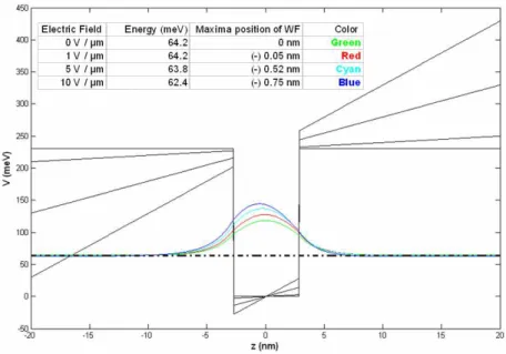
Excitonic Effects in III-Nitride Quantum Heterostructures
As mentioned in the quantum confined Stark effect section, excitons are of special im-portance for the utilization of this effect. In principle, strength of excitonic effects can be related to overlap integral of electron and hole wavefunctions. For polar III-nitride quantum structures, however, excitons are usually ionized because of the built-in po-larization induced electrostatic fields inside the well structure. In the design part, our simulation results show that when this field is compensated by the external electric field electron and hole move towards each other, enhancing excitonic effects. However, in the real case it is not usually possible to get such abrupt heterojunctions as we model in our simulations. Also, external electric field has the same direction as the polarization-induced barrier field. Because of these two, electrons and/or holes tend to tunnel out of the structure easier than we expect in our simulations. This tunnel-ing causes the diminishtunnel-ing of excitonic effects. In agreement with this argument, we
CHAPTER 4. DEVICE IMPLEMENTATION 31
can find no bound states when we increase the external electric field further in our simulations. So both polarization-induced electrostatic fields in the well and barrier structures and external electric field are against the excitonic effects. Under this trade-off, and remembering the dependence of well and barrier fields on the well-to-barrier width ratio (dbarrier/dwell), an optimal operating range would be about 1 for excitonic
effects to take place strongly. We shall re discuss these effects for our structures under the experimental results later in this chapter.
4.1.2
Epitaxial Design
In the epitaxial design, we determine the alloy content and thickness of all the layers. Our designs were based on a p-i-n diode structure with p- and n-layers that are trans-parent at the operation wavelength. In order to prevent undesired reactions between metalorganic vapors and ammonia (which cause cracks) and initiate crystallinity, we include a low temperature grown GaN or AlN nucleation layer in the beginning of the growth [24], which are also transparent at the operation wavelength. In order to obtain a high crystal quality, we introduce thick (typically 200 nm) GaN buffer layer after the nucleation layer. A typical epitaxial design is given Table (4.1).
Table 4.1: A representative epitaxial design.
No. Name Thickness Doping Loop
8 p-type GaN contact layer 120 nm Mg (max) 1
7 p-type Al0.1Ga0.9N 10 nm Mg (max) 1
6 GaN barrier 4 nm uid. 1
5 In0.1Ga0.9N well 4 nm uid. 5 (with layer 4)
4 GaN barrier 4 nm uid. 5 (with layer 5)
3 n-type GaN contact layer 700 nm Si (max) 1
2 High Temp. GaN Buffer 200 nm undoped 1
1 Low Temp. GaN Nucleation 14 nm undoped 1
CHAPTER 4. DEVICE IMPLEMENTATION 32
Figure 4.3: Layout program view of a modulator in our photomask design.
Figure 4.4: Layout program view of TLM grids in our photomask design.
4.1.3
Device Design
The device design part consists of photomask layout design for microfabrication. We designed our devices to be surface-normal, having a mesa (table-top shape) architec-ture. The devices to be characterized should have open or at least semi-transparent optical windows to be tested for their electroabsorption performances. The mesa sizes vary between 300 µm × 300 µm and 10 µm × 10 µm. A typical size of a chip can be 6mm × 6mm. The photomask includes as many devices as possible. We also designed TLM (transmission line method) grids to determine ohmic contact parasitic resistance of the devices and the resistivity of epitaxial structures. In Fig.s 4.4 and 4.3 are shown the layout program view of one of the 300 µm mesa modulators and the TLM grids, respectively.
CHAPTER 4. DEVICE IMPLEMENTATION 33
We use the same photomask for all our epitaxial structures. Having completed all the design steps, we begin our experimental work.
4.2
Experimental Work
In this section, we explain our experimental work: growth, fabrication and charac-terization. As mentioned earlier, we have grown all of our wafers on c-plane sapphire substrates using MOCVD. Device microfabrication and characterization processes were completed at class-100 and class-10.000 environments of Bilkent University Advanced Research Laboratory of the Physics Department and Nanotechnology Research Center (NANOTAM).
4.2.1
Growth
Mainly one MOCVD system was used for the growth of our modulator wafers at Bilkent NANOTAM. For the growths, we use TEGa (for quantum structures), TMIn, TMGa, TMAl and N H3 as semiconductor precursors. For n- and p-type dopant precursors, we
use SiH4 and Cp2M g, respectively. As mentioned earlier, we need a low growth rate
in the growth of quantum structures. For this purpose, as suggested in the literature, we used TEGa and a low III-V flow molar ratio [25].
The MOCVD at Bilkent NANOTAM uses LayTec EpiR reflectivity system, which simultaneously measures reflectivity at different wavelengths as an in-situ measure-ment tool. A full oscillation in reflectivity-time chart relates to the thickness of ma-terial grown within that time interval via the wavelength and refractive index of the material. This enables us to monitor the thickness of grown material and determine the growth rate. The strength of reflectivity signal is also correlated with the crys-tal quality and this gives us the chance to control and improve cryscrys-tal quality during the growth. In Fig. 4.5 is given the reflectivity measurement results of a successfully
CHAPTER 4. DEVICE IMPLEMENTATION 34
Figure 4.5: In-situ reflectivity measurement results for InGaN/GaN quantum electroabsorption modulator wafer at λ=541.4 nm where the wafer is transparent.
grown InGaN/GaN quantum modulator wafer. Grown material in each time interval is indicated on this figure.
4.2.2
Material Characterization
For the best quantum EAM operation, the grown material should meet some certain specifications such as a strong photoluminescence peak at room temperature and an RMS (root-mean-square) surface roughness of a reasonable value. When we make sure that the grown material meets these specifications, we fabricate and test the devices.
Our material characterization steps consists of atomic force microscopy (AFM) analysis for surface roughness; photoluminescence (PL) measurement for the deter-mination and quality of quantum structures; transmission measurement for bandgap determination of the bulk layer that has the widest bandgap, and secondary ion mass spectrometry (SIMS) measurement1 for the verification of materials in each layer.
1We outsource this measurement as a service from a material analysis company (HIDEN
CHAPTER 4. DEVICE IMPLEMENTATION 35
Figure 4.6: 0.5 µm × 0.5 µm atomic force microscope image taken from one of our wafers.
Fig. 4.6 shows the contact-mode AFM scan results of the wafer with the roughest surface among all our successfully grown wafers. It has 0.85 nm RMS surface roughness which is a reasonable value for our purposes.
Fig. 4.7 shows the room temperature photoluminescence (PL) spectrum obtained by our PL setup that includes a He-Cd laser with an excitation wavelength of 325 nm, and a monochromator. We observe the PL peak at 430 nm with a full width at half maximum (FWHM) of 14 nm for a 5 InGaN/GaN quantum well barrier structure. In the PL spectrum, we see both GaN (bulk) and InGaN/GaN quantum photolumines-cence, latter being stronger.
In Fig. 4.8, we see the wafer transmission spectrum obtained by a pulsed Xe light source and a spectrometer. Since the bulk layer with the widest bandgap material is GaN for this structure, we see GaN absorption edge, which is at around 360 nm.
In the SIMS depth profile of one of our wafers with 15 InGaN/GaN (4 nm/4 nm) quantum structures protected by a thin p-AlGaN layer, we see p- and i- layers. Quan-tum structures cannot be resolved clearly due to erosion effects, however total thickness of the active layer is approximately as we expected by our growth rate calculations.
CHAPTER 4. DEVICE IMPLEMENTATION 36
Figure 4.7: Photoluminescence spectrum of one of our epi-wafers
Figure 4.8: A typical wafer transmission spectrum for our InGaN/GaN quantum electroabsorption modulators.
CHAPTER 4. DEVICE IMPLEMENTATION 37
Figure 4.9: SIMS analysis results of one of our wafers with 15 InGaN/GaN quantum well/barrier structures.
CHAPTER 4. DEVICE IMPLEMENTATION 38
Figure 4.10: Device after cleaning.
Figure 4.11: Device after mesa etching.
4.2.3
Fabrication
Microfabrication process was completed in the class-100 environment of the Advanced Research Laboratory (ARL). Our fabrication started with activation of Mg dopants by keeping the whole wafer at 750oC in a nitrogen ambient. We then cleaved the chips
from the backside of the wafer as a square about one centimeter on one side, according to our photomask design. After a cleaning process that consists of ultrasonic bath in acetone and then isopropanol, each being 5 minutes, we dried the sample with a pressured nitrogen gas. We applied positive photolithography (removal of UV exposed photoresist via developer) for the definition of p-mesas and use reactive ion etching (RIE) with Freon-12 (CCl2F2) plasma to land at n-type semiconductor layer.
Subsequently, we again used positive photolithography for p-contact features. We evaporated Ni/Au (10/100 nm thick) for p-contact metallization. We used nickel for the adhesion of gold to p-type GaN . We then applied a lift-off process to remove metals that have photoresist underneath.
CHAPTER 4. DEVICE IMPLEMENTATION 39
Figure 4.12: Device after p-contact formation.
Figure 4.13: Device after n-contact formation and annealing.
For n-contacts, we again define the contacts via positive photolithography and evaporated Ti/Al (10/100 nm thick). After the n-contact lift off, we applied rapid thermal annealing for alloy formation in the metal-semiconductor interface to get ohmic contacts instead of Schottky contacts. We annealed our samples at 6000C typically for
1 minute in a nitrogen ambient. Fig. 4.14 shows a micrograph of one of the modulators we fabricated at Bilkent University.
4.2.4
Device Characterization
Our device characterization steps include electrical and optoelectronic characterization techniques. We measured the current-voltage (IV) characteristics of our devices. Since all are p-i-n diodes, they have a diode type of rectifying IV characteristics as shown in Fig. 4.15. Turn on voltage is typically about 2.5 Volts. In forward bias, we obtained electroluminescence (EL) out of our devices, with a spectrum shown in Fig. 4.16 for a
CHAPTER 4. DEVICE IMPLEMENTATION 40
Figure 4.14: Micrograph of a fabricated device.
Figure 4.15: IV curve of one of our modulators, inset shows the semilog scale IV characteristics.
![Figure 1.3: Absorption band edges of III-nitrides in the optical spectrum [9].](https://thumb-eu.123doks.com/thumbv2/9libnet/5830210.119367/21.892.177.783.131.280/figure-absorption-band-edges-iii-nitrides-optical-spectrum.webp)
![Figure 3.2: A p-i-n photodiode under reverse bias and illumination (After Ref. [16]).](https://thumb-eu.123doks.com/thumbv2/9libnet/5830210.119367/31.892.273.679.412.738/figure-p-i-photodiode-reverse-bias-illumination-ref.webp)