Full-band polar optical phonon scattering analysis and negative differential conductivity
in wurtzite GaN
C. Bulutay
Department of Physics, Bilkent University, 06533 Bilkent, Ankara, Turkey
B. K. Ridley
Department of Electronic Systems Engineering, University of Essex, Colchester C04 3SQ, United Kingdom
N. A. Zakhleniuk
Caswell Technology, Marconi Caswell, Towcester, Northants, NN12 8EQ, United Kingdom 共Received 27 March 2000; revised manuscript received 5 July 2000兲
GaN has promising features for high-field electronics applications. To scrutinize these transport-related properties, primarily the dominant scattering mechanism in this material needs to be well characterized. In the quest for Bloch oscillations in bulk GaN, our aim is to conduct a full-band scattering analysis requiring very high energies where parabolic approximation is far from applicable. For this purpose, we first obtain an accurate band structure for the conduction band of wurtzite GaN based on the empirical pseudopotential method, using the most recent experimental data as the input. We compute the scattering rate, relevant up to room temperatures, due to longitudinal-optical-like and transverse-optical-like polar phonon modes along several共high-symmetry兲 directions, from the conduction band minimum at the zone center to the half of the reciprocal lattice vector in each direction. We observe that the location and the symmetry of the neighboring valleys to the route play a decisive role on the scattering rates. The observation of Bloch oscillations in bulk wurtzite GaN is doomed by the very large value of the polar scattering rate. However, there exists the possibility of a negative differential conductivity driven by the negative effective mass part of the band structure for fields above 2.3 MV/cm for wurtzite GaN.
I. INTRODUCTION
In the last decade GaN and other related III nitrides have been a subject of intensive research, initiated by their out-standing optoelectronic prospects, such as light emitting di-odes, and lasers in the visible spectrum.1The fact that these III nitrides are wide bandgap materials, also make them very attractive for electronic applications, especially for high-power and high-temperature purposes. The ability of these III nitrides to withstand very high electric fields on the order of few MV/cm, brings new possibilities, not within reach of the traditional semiconductors such as Si and GaAs. One intriguing possibility is to observe the elusive Wannier-Stark resonances and the associated Bloch oscillations in a bulk semiconductor, such as GaN.2,3 Such a study requires a de-tailed knowledge of the transport properties in these wide bandgap materials, primarily the characterization of the dominant scattering mechanism. This, in GaN is the polar optical phonon scattering due to its high degree of ionicity4 and hence large electron-phonon coupling constant.
The aim of this paper is to quantitatively analyze the full conduction band electron scattering rates due to polar optical phonon共POP兲 emission. We obtain these scattering rates in several different directions in the reciprocal lattice, from the conduction band minimum to the half of the reciprocal lattice vector in that direction. This comparative study also pro-duces a valuable output for the likelihood of the Wannier-Stark resonances in bulk wurtzite 共WZ兲 GaN. For the accu-racy of our results we base our analysis on realistic models for both electrons and phonons in WZ GaN.
The full-band scattering rate requires a reliable band en-ergy and wave function knowledge. Empirical pseudopoten-tial method 共EPM兲5 is widely used for such purposes and several results for GaN have already been published.6–10We have analyzed these proposed band structures and found them to be unsatisfactory for the conduction band properties, such as the conduction band effective mass and also in the agreement to the more recently released experimental data on the conduction band energies.11,12As this point is of central importance in our work, we have also performed an EPM study for WZ GaN, demanding a close fit to these conduction band properties. Based on this band structure, as a by-product we present the energy levels and effective mass pa-rameters of the conduction band satellite valleys, which play important role in high-field electronic transport properties.
Formally, the electron-phonon coupling in WZ GaN is different from the well-known cubic case, bringing in longi-tudinal optical 共LO兲-like and transverse optical 共TO兲-like modes,13 rather than a single LO mode as in a zinc blende crystal having an isotropic phonon spectrum. We analyze both of these modes and observe the TO-like scattering rate to be more than two orders of magnitude lower than the LO-like modes. Furthermore, we find the LO scattering rate in the cubic approximation to be in very good agreement with the LO-like case, regardless of the chosen point in the Brillouin zone 共BZ兲.
The symmetry of the initial- and final-state electron wave functions plays an important role in the correct assessment of the scattering rates. Indeed, we observe that above the energy of the lowest satellite valley U3,minthe rates are significantly PRB 62
overestimated if the cell-periodic overlap is taken as unity, which actually works well only in the vicinity of the conduc-tion band minimum. Based on these direcconduc-tional scattering rates we investigate the high-field negative differential con-ductivity possibilities.
In the next section, we present our guidelines and results for the band structure fitting, concentrating on the conduction band properties. In Sec. III the formulation for the POP scat-tering for the WZ crystal is given. Our results are contained in Sec. IV, followed by a discussion in Sec. V on the impli-cations of these results in connection to Bloch oscillations and negative differential conductivity. A brief summary is given in Sec. VI. The Appendix discusses two different implementations of computing the scattering rate over the BZ.
II. BAND STRUCTURE FITTING FOR THE CONDUCTION BAND
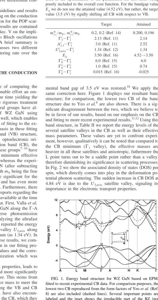
EPM admirably suits to our purpose of computing the scattering rate, as it provides with reasonable effort an em-pirically tailored band profile at the same time yielding the pseudowave functions necessary for the rigorous treatment of the transition matrix elements. Several groups have al-ready obtained the band structure of WZ GaN using EPM,6–10reporting their form factors as well, which enables other researchers to circumvent the task of fitting to the ex-perimental values. Apparently, the emphasis in these fitting procedures has been on the valence band 共VB兲 structure, predominantly due to its importance in optoelectronic ori-ented applications. As for the conduction band 共CB兲, the fitted EPM band structure reported by these groups7–10have important drawbacks; notably, the CB minimum effective mass comes out to be 0.15 m0 or less, whereas the experi-mentally measured14 value for WZ GaN 共after subtracting the polaronic contribution兲 is 0.2 m0, with m0 being the free electron mass. This discrepancy is quite significant for the low-field electronic transport properties and has even more drastic consequences for higher energies. Furthermore, there have been two very recent experimental reports regarding the band structure of the CB which were not available at the time the previous EPM works were carried out. First, Valla et al. have measured the CB structure of WZ GaN along the⌫-A direction in the BZ using the inverse photoemission techniques.11 Secondly, Sun et al.12 analyzing the ultrafast electron dynamics in n-doped GaN have reported the energy separation between the lowest satellite valley U3,min along the U symmetry line and the CB minimum 共as 1.34 eV兲. In the lack of any further verification of these results, we com-ply with these experiments and use them in our fitting pro-cedure. Table I lists the chosen target values and the corre-sponding attained values by the optimization which was based on the Metropolis algorithm.17
The fact that we have favored the CB properties, leads to some discrepancy in the VB structure and more significantly the bandgap value comes out 1 eV higher. This stems from the requirement of a heavier CB effective mass to meet the experimental value that results in pushing the VB and CB apart. As a matter of fact, Kolnı´k et al. have also encoun-tered this problem in their EPM fitting to the CB, which they remedied by rigidly shifting the CB, so that the true
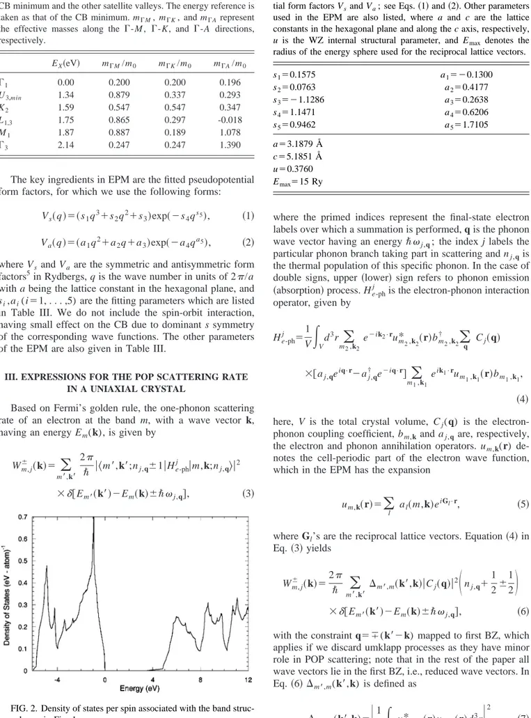
experi-mental band gap of 3.5 eV was restored.18 We apply the same correction here. Figure 1 displays our resultant band structure; for comparison, the lowest two CB of the band structure due to Yeo et al.8 are also shown. There is a sig-nificant disagreement between the two, which we believe to be in favor of our results, based on our emphasis on the CB and fitting to more recent experimental results.11,12Using this band structure, in Table II we report the energy levels of the several satellite valleys in the CB as well as their effective mass parameters. These values are yet to confront experi-ment, however, qualitatively it can be noted that compared to the CB minimum (⌫1 valley兲, the effective masses are heavier in all these satellites and anisotropic, futhermore the L point turns out to be a saddle point rather than a valley, therefore diminishing its significance in scattering processes. In Fig. 2 we show the associated density of states共DOS兲 per spin, which directly comes into play in the deformation po-tential phonon scattering. The sudden increase in CB DOS at 4.84 eV is due to the U3,min satellite valley, signaling its importance in the electronic transport properties.
TABLE I. Target values based on the quoted references and the attained values by our optimization. All energies are given in eV. The lineup from top to bottom crudely represents the emphasis we used in the optimization of the parameters, the last items being poorly included to the overall cost function. For the bandgap value Egwe do not use the attained value共4.52 eV兲, but rather, the target
value共3.5 eV兲 by rigidly shifting all CB with respect to VB.
Target Attained mc*⬜/m0, mcz*/m0 0.2, 0.2共Ref. 14兲 0.200, 0.196 ⌫3 c⫺⌫ 1 c 2.13共Ref. 11兲 2.14 A1,3 c ⫺⌫ 1 c 3.0共Ref. 11兲 2.52 U3,min c ⫺⌫1 c 1.34共Ref. 12兲 1.34 Eg 3.50共Ref. 16兲 4.52→3.50 ⌫6v⫺⌫3v 6.0共Ref. 15兲 6.0 ⌫6 v⫺⌫ 5 v 1.0共Ref. 15兲 0.74 ⌫6 v⫺⌫ 1 v 0.015共Ref. 16兲 -0.025
FIG. 1. Energy band structure for WZ GaN based on EPM, fitted to recent experimental CB data. For comparison purposes, the lowest two CB reproduced from the form factors of Yeo et al.共Ref. 8兲 are also included 共dashed lines兲. Several important points are labeled and the inset shows the irreducible part of the BZ 共not drawn to scale兲.
The key ingredients in EPM are the fitted pseudopotential form factors, for which we use the following forms:
Vs共q兲⫽共s1q3⫹s2q2⫹s3兲exp共⫺s4qs5兲, 共1兲
Va共q兲⫽共a1q2⫹a
2q⫹a3兲exp共⫺a4qa5兲, 共2兲 where Vs and Va are the symmetric and antisymmetric form factors5in Rydbergs, q is the wave number in units of 2/a with a being the lattice constant in the hexagonal plane, and
si,ai(i⫽1, . . . ,5) are the fitting parameters which are listed in Table III. We do not include the spin-orbit interaction, having small effect on the CB due to dominant s symmetry of the corresponding wave functions. The other parameters of the EPM are also given in Table III.
III. EXPRESSIONS FOR THE POP SCATTERING RATE IN A UNIAXIAL CRYSTAL
Based on Fermi’s golden rule, the one-phonon scattering rate of an electron at the band m, with a wave vector k, having an energy Em(k), is given by
Wm, j⫾ 共k兲⫽
兺
m⬘,k⬘ 2 ប 兩具
m⬘
,k⬘
;nj,q⫾1兩He-ph j 兩m,k;n j,q典
兩2 ⫻␦关Em⬘共k⬘
兲⫺Em共k兲⫾បj,q兴, 共3兲where the primed indices represent the final-state electron labels over which a summation is performed, q is the phonon wave vector having an energyបj,q; the index j labels the particular phonon branch taking part in scattering and nj,qis the thermal population of this specific phonon. In the case of double signs, upper 共lower兲 sign refers to phonon emission 共absorption兲 process. He-ph
j is the electron-phonon interaction operator, given by He-phj ⫽1 V
冕
V d3r兺
m2,k2 e⫺ik2•ru m2,k2 * 共r兲bm 2,k2 †兺
q Cj共q兲 ⫻关aj,qeiq•r⫺aj,q † e⫺iq•r兴兺
m1,k1 eik1•ru m1,k1共r兲bm1,k1, 共4兲 here, V is the total crystal volume, Cj(q) is the electron-phonon coupling coefficient, bm,kand aj,q are, respectively, the electron and phonon annihilation operators. um,k(r) de-notes the cell-periodic part of the electron wave function, which in the EPM has the expansionum,k共r兲⫽
兺
lal共m,k兲eiGl•r, 共5兲 where Gl’s are the reciprocal lattice vectors. Equation共4兲 in Eq. 共3兲 yields Wm, j⫾ 共k兲⫽2 ប m
兺
⬘,k⬘ ⌬m⬘,m共k⬘
,k兲兩Cj共q兲兩2冉
nj,q⫹ 1 2⫾ 1 2冊
⫻␦关Em⬘共k⬘
兲⫺Em共k兲⫾បj,q兴, 共6兲 with the constraint q⫽⫿(k⬘
⫺k) mapped to first BZ, which applies if we discard umklapp processes as they have minor role in POP scattering; note that in the rest of the paper all wave vectors lie in the first BZ, i.e., reduced wave vectors. In Eq. 共6兲 ⌬m⬘,m(k⬘
,k) is defined as ⌬m⬘,m共k⬘
,k兲⫽冏
1 ⍀冕
⍀um⬘,k⬘ * 共r兲um,k共r兲d3r冏
2 , 共7兲TABLE II. The energy and the effective mass parameters of the CB minimum and the other satellite valleys. The energy reference is taken as that of the CB minimum. m⌫M, m⌫K, and m⌫Arepresent the effective masses along the ⌫-M, ⌫-K, and ⌫-A directions, respectively. EX共eV兲 m⌫M/m0 m⌫K/m0 m⌫A/m0 ⌫1 0.00 0.200 0.200 0.196 U3,min 1.34 0.879 0.337 0.293 K2 1.59 0.547 0.547 0.347 L1,3 1.75 0.865 0.297 -0.018 M1 1.87 0.887 0.189 1.078 ⌫3 2.14 0.247 0.247 1.390
FIG. 2. Density of states per spin associated with the band struc-ture shown in Fig. 1.
TABLE III. Fitted values for the constants in the pseudopoten-tial form factors Vsand Va; see Eqs.共1兲 and 共2兲. Other parameters
used in the EPM are also listed, where a and c are the lattice constants in the hexagonal plane and along the c axis, respectively, u is the WZ internal structural parameter, and Emax denotes the radius of the energy sphere used for the reciprocal lattice vectors.
s1⫽0.1575 a1⫽⫺0.1300 s2⫽0.0763 a2⫽0.4177 s3⫽⫺1.1286 a3⫽0.2638 s4⫽1.1471 a4⫽0.6206 s5⫽0.9462 a5⫽1.7105 a⫽3.1879 Å c⫽5.1851 Å u⫽0.3760 Emax⫽15 Ry
where the integration is over the primitive cell volume, ⍀. Using Eq. 共5兲, the above integration turns into a summation over the reciprocal lattice vectors as
⌬m⬘,m共k
⬘
,k兲⫽冏
兺
lal*共m
⬘
,k⬘
兲al共m,k兲冏
2, 共8兲
with the al’s readily computed by EPM.
As the WZ structure belongs to the class of uniaxial crys-tals, the electron-polar optical phonon coupling coefficient is formally different from the well-known cubic 共Fro¨hlich兲 form.20For the case of a weakly anisotropic uniaxial crystal, Lee and co-workers21 have obtained the following approxi-mate forms for the coupling coefficients of the longitudinal-optical共LO兲-like and transverse-optical 共TO兲-like modes
兩Cq LO-like兩2⯝ 2e 2ប Vq2⍀L共q兲 ⫻
冋
sin 2 q冉
1 ⑀⬜⬁ ⫺ 1 ⑀⬜0冊
⬜L2 ⫹ cos 2 q冉
1 ⑀z⬁ ⫺1 ⑀z 0冊
zL 2册
⫺1 , 共9兲 兩Cq TO-like兩2 ⫽ 2e 2ប Vq2⍀T共q兲 共⬜2⫺ z 2兲2sin2 qcos2q 共⑀⬜0⫺⑀⬜⬁兲⬜2cos2q⫹共⑀z 0⫺⑀ z ⬁兲 z 2sin2q, 共10兲 whereqis the angle phonon wave vector, q makes with the crystal c axis,⬜(z) is the TO phonon frequency perpen-dicular to 共along兲 the c axis, ⬜L(zL) is the LO phonon frequency perpendicular to 共along兲 the c axis,⑀⬜⬁(⑀z⬁) is the high frequency dielectric constant perpendicular to 共along兲 the c axis. The corresponding static dielectric constants are given by ⑀⬜0⫽⑀⬜⬁⬜L2 /⬜2 and ⑀z0⫽⑀z⬁zL2 /z2. The phonon frequency,j,q, in Eq.共6兲 is now replaced for the LO-like and TO-like modes by ⍀L(q) and ⍀T(q), respectively, given by13 ⍀L共q兲⫽冑
zL 2 cos2q⫹⬜L2 sin2q, 共11兲 ⍀T共q兲⫽冑
z 2 sin2q⫹⬜ 2 cos2q. 共12兲The nonzero TO-like coupling coefficient is due to the LO ingredient in this mode; its contribution vanishes for the iso-tropic case when ⬜⫽z and ⬜L⫽zL, where the cubic form is restored.
The quantity, Wm(k) gives the rate for an electron that belongs to band m, with a wave vector k; for brevity, here we suppress some of the subscripts and superscripts. We can also introduce the following quantity that replaces the
mag-nitude of k with the energy, while retaining the band index
and the direction in the BZ, as
W˜mkˆ共E兲⫽
兺
pWm共p兲␦共kˆ•pˆ⫺1兲␦关E⫺Em共p兲兴
兺
p␦共kˆ•pˆ⫺1兲␦关E⫺Em共p兲兴, 共13兲
where pˆ and kˆ represent unit vectors in the direction of p and
k, respectively. The denominator equals the number of
crossings22 of the value E by the constant energy surface of the band m along the vector kˆ. The explicit energy depen-dence offered by W˜ is sometimes more illuminating, and in our case it also enables direct comparison of the rates along different directions in the BZ.
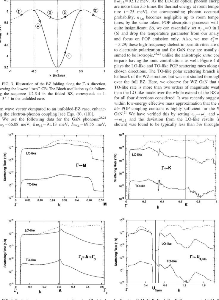
IV. DIRECTIONAL POP SCATTERING RATES Based on the acceleration theorem,19 carriers in a band under an electric field F obey the relation eF⫽បk˙. That is, carriers follow the trajectory along the field direction in the reciprocal space until a scattering event takes place, the dominant one being POP scattering in GaN due to its high ionicity.4 Note that, the scattering rate formulation in the previous section does not address an electric field. Indeed, Bardeen and Shockley23 have asserted that, acceleration of electrons by a uniform applied field, and scattering by lattice vibrations or imperfections are independent processes by showing that although the details of the transition may be altered by the electric field, the final expressions for the scat-tering rate are independent of the field.24,25Accordingly, we trace the POP scattering rate of CB electrons along the high-symmetry directions, starting from CB minimum (⌫1) until half of the corresponding reciprocal lattice vector 共RLV兲 along the lines ⌫-M, ⌫-K, and ⌫-A, as well as along the ⌫-U3,min direction as this route connects the lowest two minima in the CB.26 The trajectories along ⌫-K and ⌫-U3,min require longer RLVs and extend beyond the first BZ boundary. Another technical detail here is that EPM la-bels the bands by sorting their energies at each k point, re-gardless of the actual continuation of the bands beyond the band crossings.27This point is particularly important for the band along the ⌫-K direction. For such crossing bands, we compare the values of the overlap parameter ⌬m⬘,m, given by Eqs. 共7兲, 共8兲 and determine which way the band actually continues. Further details about the implementation of the computation are given in the Appendix. A rewarding use of the overlap test is along the⌫-A direction, which reveals that there is actually a BZ folding at the A point. This is due to four-layer stacking of the gallium and nitrogen atoms along the c axis.29So, an electron from the lower CB reaching the BZ boundary (k⫽zˆ/c) continues, in the reduced band scheme, to the upper band, starting from the point ⫺zˆ/c. The Bloch oscillation cycle and the BZ folding effect are illustrated in Fig. 3. Hence, in tracing the scattering rate along this direction, we take this fact into account and follow the extended trajectory ⌫1-A⫺⌫3, corresponding to seg-ments 1⫺2 in Fig. 3. The presence of the BZ folding modi-fies the POP scattering rates as the valley along the ⌫-A direction is now mapped back to ⌫ point 共i.e., ⌫3 valley兲, which somewhat increases the scattering rate to this valley from directions such as⌫-M, due to a smaller required
pho-non wave vector compared to an unfolded-BZ case, enhanc-ing the electron-phonon couplenhanc-ing关see Eqs. 共9兲, 共10兲兴.
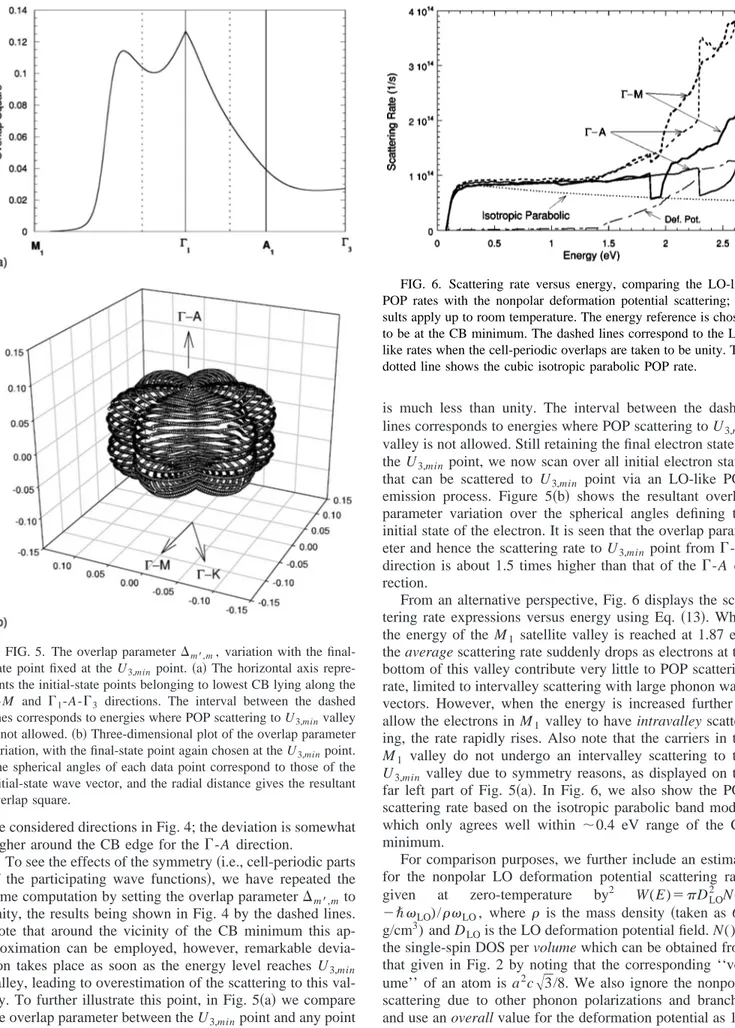
We use the following data for the GaN phonons:28,21 បz⫽66.08 meV, បzL⫽91.13 meV, ប⬜⫽69.55 meV,
ប⬜L⫽92.12 meV. As the LO-like optical phonon energies
are more than 3.5 times the thermal energy at room tempera-ture (⬃25 meV兲, the corresponding phonon occupation probability, nj,q becomes negligible up to room tempera-tures; by the same token, POP absorption processes will be quite insignificant. So, we can essentially set nj,q⬅0 in Eq. 共6兲 and drop the temperature parameter from our analysis and focus on POP emission only. Also, we use ⑀⬜⬁⫽⑀z⬁ ⫽5.29; these high-frequency dielectric permittivities are due to electronic polarization and for GaN they are usually as-sumed to be isotropic,28,21unlike the anisotropic static coun-terparts having the ionic contributions as well. Figure 4 dis-plays the LO-like and TO-like POP scattering rates along the chosen directions. The TO-like polar scattering branch is a hallmark of the WZ structure, but was not studied thoroughly over the full BZ. Here, we observe for WZ GaN that the TO-like rate is more than two orders of magnitude weaker than the LO-like mode over the whole extend of the BZ and for all four directions considered. It was recently suggested within low-energy effective mass approximation that the
cu-bic POP coupling constant is highly sufficient for the WZ
GaN.21 We have verified this by setting z→⬜ and zL
→⬜L and the deviation from the LO-like results 共not
shown兲 was found to be typically less than 5% throughout FIG. 3. Illustration of the BZ folding along the⌫-A direction,
showing the lowest ‘‘two’’ CB. The Bloch oscillation cycle follow-ing the sequence 2-3-4 in the folded BZ, corresponds to 1-2⬘-3⬘-4 in the unfolded case.
FIG. 4. Scattering rate versus wave vector共in units of 2/a) along the directions ⌫-M, ⌫-K, ⌫1-A-⌫3, ⌫-U3,mincomputed till half of the corresponding RLV; results apply up to room temperature. The dashed lines indicate the LO-like rates when the cell-periodic overlaps are taken to be unity.
the considered directions in Fig. 4; the deviation is somewhat higher around the CB edge for the⌫-A direction.
To see the effects of the symmetry共i.e., cell-periodic parts of the participating wave functions兲, we have repeated the same computation by setting the overlap parameter⌬m⬘,mto unity, the results being shown in Fig. 4 by the dashed lines. Note that around the vicinity of the CB minimum this ap-proximation can be employed, however, remarkable devia-tion takes place as soon as the energy level reaches U3,min valley, leading to overestimation of the scattering to this val-ley. To further illustrate this point, in Fig. 5共a兲 we compare the overlap parameter between the U3,minpoint and any point along the ⌫-A and ⌫-M directions. The primary purpose of this figure is to show that the actual overlap with U3,minpoint
is much less than unity. The interval between the dashed lines corresponds to energies where POP scattering to U3,min valley is not allowed. Still retaining the final electron state as the U3,min point, we now scan over all initial electron states that can be scattered to U3,min point via an LO-like POP emission process. Figure 5共b兲 shows the resultant overlap parameter variation over the spherical angles defining the initial state of the electron. It is seen that the overlap param-eter and hence the scattering rate to U3,min point from⌫-M direction is about 1.5 times higher than that of the ⌫-A di-rection.
From an alternative perspective, Fig. 6 displays the scat-tering rate expressions versus energy using Eq. 共13兲. When the energy of the M1 satellite valley is reached at 1.87 eV, the average scattering rate suddenly drops as electrons at the bottom of this valley contribute very little to POP scattering rate, limited to intervalley scattering with large phonon wave vectors. However, when the energy is increased further to allow the electrons in M1 valley to have intravalley scatter-ing, the rate rapidly rises. Also note that the carriers in the
M1 valley do not undergo an intervalley scattering to the
U3,min valley due to symmetry reasons, as displayed on the far left part of Fig. 5共a兲. In Fig. 6, we also show the POP scattering rate based on the isotropic parabolic band model, which only agrees well within ⬃0.4 eV range of the CB minimum.
For comparison purposes, we further include an estimate for the nonpolar LO deformation potential scattering rate, given at zero-temperature by2 W(E)⫽DLO2 N(E
⫺បLO)/LO, where is the mass density 共taken as 6.1 g/cm3) and DLOis the LO deformation potential field. N() is the single-spin DOS per volume which can be obtained from that given in Fig. 2 by noting that the corresponding ‘‘vol-ume’’ of an atom is a2c
冑
3/8. We also ignore the nonpolar scattering due to other phonon polarizations and branches and use an overall value for the deformation potential as 109 eV/cm, which applies to GaAs intervalley transitions. The resultant nonpolar rate is seen to be well below the POP rate FIG. 5. The overlap parameter⌬m⬘,m, variation with thefinal-state point fixed at the U3,minpoint.共a兲 The horizontal axis
repre-sents the initial-state points belonging to lowest CB lying along the ⌫-M and ⌫1-A-⌫3 directions. The interval between the dashed
lines corresponds to energies where POP scattering to U3,minvalley
is not allowed.共b兲 Three-dimensional plot of the overlap parameter variation, with the final-state point again chosen at the U3,minpoint.
The spherical angles of each data point correspond to those of the initial-state wave vector, and the radial distance gives the resultant overlap square.
FIG. 6. Scattering rate versus energy, comparing the LO-like POP rates with the nonpolar deformation potential scattering; re-sults apply up to room temperature. The energy reference is chosen to be at the CB minimum. The dashed lines correspond to the LO-like rates when the cell-periodic overlaps are taken to be unity. The dotted line shows the cubic isotropic parabolic POP rate.
over a great portion of the energies of the lowest CB. How-ever, a strict quantitative comparison is not very reliable, given the gross uncertainity in the deformation potential field values for GaN and the simplistic treatment used here for the deformation potential scattering.
V. IMPLICATIONS ON BLOCH OSCILLATIONS AND NEGATIVE DIFFERENTIAL CONDUCTIVITY
A. Bloch oscillations
Our investigation of the full-band directional scattering analysis in GaN leads to some implications about the Bloch oscillations and the negative differential conductivity. Though, in superlattices these Bloch oscillations were ob-served through optical experiments 共for a review see, e.g., Ref. 30兲, it is yet to be seen in transport experiments31and in
bulk semiconductors. The existence of Bloch oscillations is
possible in a window of electric fields, limited from below by the scattering mechanisms, breaking the phase memory of the participating electrons, and from above by the escape of the electron to other bands or the breakdown of the material by Zener or impact ionization mechanisms. Our work here can only address the lower limit set on the electric field by the dominant scattering mechanism, this being the LO-phonon emission up to room temperatures. As for the break-down voltage, wide bandgap semiconductors, such as III ni-trides 共such as GaN兲 presumably offer higher breakdown values, tempting further research in this direction.3
Bloch oscillation corresponds to the traversal of an elec-tron along a RLV from one reciprocal lattice point to another forming a repetitive motion. Strictly speaking this regime requires the applied electric field direction to coincide with a RLV. Under these circumstances, if the magnitude of the shortest RLV along the field direction is兩G兩, then the Bloch angular frequency simply follows from the acceleration theo-rem asB⫽2eF/ប兩G兩. For the case of the WZ crystal, the
two shortest RLVs are along ⌫-M and ⌫-A directions with the magnitudes 4/a
冑
3 and 2/c, respectively. However, for the ⌫-A direction, twice this value 共hence 4/c) needs to be considered due to BZ folding effect共see Fig. 3兲.The criterion for the observation of Bloch oscillations shows some variation over the literature.19,30,32–36A common expression19,30,32isB⬎1, which is based on the fact that the associated Wannier-Stark level spacing បB being greater than the level broadening, ប/ due to scattering, where is the 共maximum兲 scattering time within the band. Instead, von Plessen et al.33 suggest ប/ to be replaced by ⌫hom⫽2ប/, which is the homogeneous linewidth related to scattering time . A rather more strict criterion put forward by Esaki and Tsu isB⬎2, which requires the electron to complete one cycle in the BZ before undergoing a scattering event.34If we adopt this last criterion by Esaki and Tsu, then the threshold field for the onset of the the Bloch oscillations turns out to be well above 10 MV/cm, which cannot be at-tained due to the dielectric breakdown of the material.
B. Negative differential conductivity
A precursor of Bloch oscillations is the negative differen-tial conductivity共NDC兲 at lower fields. There have already
been several predictions of NDC in GaN 共Refs. 37– 39,18,40兲 at field levels of around 150 kV/cm, all being based on the transfer of electrons to upper valleys, which was also experimentally verified with reasonable agreement.41On the other hand, the NDC that here we refer to, is driven by the band structure’s negative effective mass part beyond the inflection point of its dispersion curve, an idea that goes back to Kro¨mer.42 Esaki and Tsu have later discussed this mechanism of NDC for the case of superlattices.34For this reason, it can be distinguished as the Kro¨mer-Esaki-Tsu NDC. Recently, the possibility of this mechanism over the valley transfer one was advocated for the case of cubic GaN.43
The dependence of drift velocity on the applied electric field can easily be estimated by the simple approach used by Esaki and Tsu for superlattices.34 Hence, the average drift velocity assuming a constant scattering time is given by
vd⫽eFប⫺2
冕
0 ⬁2E Fld kFld2 e ⫺t/dt, 共14兲 where2EFld/kFld 2is the curvature of the energy band dia-gram along the applied field’s direction F, sampled at the k point, kFld(t)⫽eFt/ប, for an electron originating from the ⌫ point. For the scattering time in this equation, we use the value given by the maximum scattering rate in Fig. 4 in each direction. Figure 7 shows the corresponding drift velocity dependence on the electric field. The different low-field mo-bilities are the artifact of using the maximum scattering rate of each direction throughout the band. Actually, this low-field part of the drift velocity is governed by the momentum relaxation time, and of course, it is not described correctly by the Esaki-Tsu formula Eq. 共14兲. However, the concept of momentum relaxation time refers to a distribution of par-ticles and is not relevant in the present context of high-field transport which is to do with the probability of avoiding collision and hence with the bare scattering time. With this reservation, Esaki-Tsu formula results are plotted for all the fields and therefore, only the high-field regime, above ⬃1 MV/cm part should be considered. It is seen that the NDC has a significant dependence on the chosen direction of trans-port and needs high electric fields, above 2.3 MV/cm. A very FIG. 7. High-field drift velocity dependence along four different directions. The⌫-M and ⌫-A curves almost coincide.
recent experiment,44measuring the steady-state drift velocity in GaN has gone up to an electric field of 350 kV/cm. Es-sentially a constant drift velocity of 2⫻107 cm/s for fields above 200 kV/cm has been extracted. Our preliminary esti-mations in Fig. 7 suggest a substantial increase in the drift velocity at field levels about a few MV/cm. This may have an important practical implication for GaN-based high-power devices, so further experiments at such high fields will be very valuable to investigate this possibility.
VI. SUMMARY
In summary, we have obtained the band structure and the associated Bloch wave functions of WZ GaN using EPM paying due attention to CB properties in light of recent ex-periments. The merits and flaws of this band structure can be assessed experimentally by verifying our resultant data char-acterizing the CB satellite valleys. Using this band structure we analyzed the full-band LO-like and TO-like POP scatter-ing rates along several important directions in the BZ. We have demonstrated the key roles played by the satellite val-leys and the symmetry of the participating wave functions. More elaborate high-field transport calculations and experi-ments for bulk GaN will be very useful in further exploring the NDC possibilities. Our rough estimation suggests the threshold field for NDC in WZ GaN to be about 2.3 MV/cm.
ACKNOWLEDGMENTS
This work was supported by Grant Nos. ONR 共N00014-99-1-0014兲 and EPSRC 共GR/L/56725兲.
APPENDIX: COMPUTATION OF THE FULL-BAND SCATTERING RATE
1. By direct integration
We compute the scattering rate given by Eq. 共6兲 in two alternative ways which agree with each other within numeri-cal accuracy. The first approach is to follow a direct integra-tion of the rate expression. As the initial standard step, the summation (兺k⬘) in this equation is converted to integration
关V/(2)3兰d3k
⬘
兴, the integration domain being the first BZwhich is hexagonal in WZ structures. We enclose this hex-agonal BZ by a cylindrical box with radius 4/3a and height 2/c, and work in cylindrical coordinates for all the wave vectors. We discard the regions of the cylinder that lies out-side the hexagonal BZ by inserting a function ⌰BZ, in the integrand共see the expressions below兲. In the rest of this sub-section, we normalize all energies to atomic Rydbergs, the component of wave vectors in the hexagonal plane to 2/a and the component along the c axis共which we choose to be along the z axis兲 to 2/c. With these manipulations and after applying the delta function property together with the asso-ciated coupling coefficients关Eqs. 共9兲, 共10兲兴, Eq. 共6兲 becomes
Wm, LO-like⫾ 共k兲⫽2aB c
冕
0 2 d⬘
冕
⫺1/2 1/2 dkz⬘
兺
i k⬜i⬘
q⬜i2 ⫹冉
a c冊
2 qzi2冉
nL,qi⫹ 1 2⫾ 1 2冊
⌰冉
23⫺k⬜i⬘
冊
冏
fL k⬜i⬘
冏
⌰BZ共k⬜i⬘
,⬘
兲 ⌬m⬘,m共ki⬘
,k兲 ⍀L共qi兲 ⫻冋
sin 2 qi冉
1 ⑀⬜⬁ ⫺ 1 ⑀⬜0冊
⬜L2 ⫹ cos 2 qi冉
1 ⑀z⬁ ⫺ 1 ⑀z 0冊
zL 2册
⫺1 , 共A1兲 Wm,TO-like⫾ 共k兲⫽2aB c冕
0 2 d⬘
冕
⫺1/2 1/2 dkz⬘
兺
i k⬜i⬘
q⬜i2 ⫹冉
a c冊
2 qzi2冉
nT,qi⫹ 1 2⫾ 1 2冊
⌰冉
2 3⫺k⬜i⬘
冊
冏
fT k⬜i⬘
冏
⌰BZ共k⬜i⬘
,⬘
兲 ⫻ ⌬m⬘,m共ki⬘
,k兲共⬜ 2⫺ z 2兲2sin2q icos 2 qi ⍀T共qi兲关共⑀⬜ 0⫺⑀ ⬜⬁兲⬜2cos2qi⫹共⑀z 0⫺⑀ z ⬁兲 z 2 sin2qi兴 , 共A2兲where aB is the atomic Bohr radius, ki
⬘
with the correspond-ing cylindrical components (k⬜i⬘
,⬘
,kz⬘
) is the ith zero of the function fL,T⫽Em⬘(k⬘
)⫺Em(k)⫾ប⍀L,T and qi⫽⫿(ki⬘
⫺k) mapped to first BZ; ⌰ is the step 共Heaviside兲 function and ⌰BZ is the function that yields 1 共0兲 if k⬜i
⬘
lies inside 共outside兲 the first hexagonal BZ. For the special cases of the initial-state electron wave vector k, we have certain simpli-fications due to symmetry: if kz⬅0, then 兰⫺1/21/2 dkz
⬘
→2兰0 1/2dk z⬘
, and if k⬅zˆkz, then兰02d⬘
→12兰0/6d⬘
. The computational bottleneck lies in finding the zeros of the function fL,T. Here, we employ the linear tetrahedron interpolation of the band energies.45 For this purpose, we store the CB energies by sampling the irreducible BZ 共IBZ兲 with 22 050 data points, giving more emphasis to the vicinity of the ⌫ point. The cell-periodic Bloch overlap function ⌬m⬘,m is smoother共see Fig. 5兲, and a 910-point final-statesampling over the IBZ is used. Note that ⌬m⬘,m does not require the phase information of the final state and only IBZ is sufficient for tabulating this function, whereas in Monte Carlo simulations the correct phase in other portions of the BZ needs to be generated to trace each particle.46,27Finally, we include the lowest four CB for the summation over the final-state bands m
⬘
in Eq.共6兲. Actually only two bands are sufficient for all the considered directions but the⌫-K direc-tion, which goes up in energy after a band crossing共see Fig. 1兲.2. By the Lehmann-Taut technique
The first approach utilizes the division of the IBZ into small tetrahedra simply for the interpolation of the energy and overlap parameters. Alternatively, using this infrastruc-ture, the tetrahedron integration technique of Lehmann and Taut45can be applied for the overall computation of the scat-tering rate. For this purpose, Eq.共6兲 can be put into the form
W⫾j,m共k兲⫽
兺
m⬘冕
S dS Wˆj,m⫾ ⬘共k⬘
兲 兩ⵜk⬘Em⬘k⬘
兩 , 共A3兲 where Wˆj,m ⬘ ⫾ 共k⬘
兲⫽2 ប V 共2兲3⌬m⬘,m共k⬘
,k兲兩Cj共q兲兩 2冉
n j,q⫹ 1 2⫾ 1 2冊
. 共A4兲 The integration is over the surface S described by the energy conservation relation of one-phonon-emission–absorption process, Em⬘(k⬘
)⫽Em(k)⫿បj,q. Equation 共A3兲 is in the form for which Lehmann-Taut algorithm45 is directly appli-cable. Accordingly, the IBZ is divided into fine tetrahedra; the grid sizes for the storage of energy and overlap param-eters are given in the previous subsection. However, the quantity Wˆ⫾j,m⬘(k⬘
) needs much finer tetrahedra共about half a million兲 but need not be stored in the memory as it can be very easily calculated in real time. We have observed the Lehmann-Taut technique to be much more robust and com-putationally efficient than the previously explained direct in-tegration approach.1S. Nakamura and G. Fasol, The Blue Laser Diode共Springer,
Ber-lin, 1997兲.
2B. K. Ridley, in Gallium Nitride and Related Materials II, edited
by C. R. Abernathy, H. Amano, and J. C. Zolper, MRS Sympo-sia Proceedings No. 468 共Materials Research Society, Pitts-burgh, 1997兲, p. 231.
3B. K. Ridley, J. Phys.: Condens. Matter 10, L607共1998兲. 4A. Garcı´a and M. L. Cohen, Phys. Rev. B 47, 4215共1993兲; 47,
4221共1993兲.
5M. L. Cohen and V. Heine, Solid State Physics: Advances in
Research and Applications, edited by H. Ehrenreich, F. Seitz, and D. Turnbull共Academic, New York, 1970兲, Vol. 24.
6S. Bloom, J. Phys. Chem. Solids 32, 2027共1971兲.
7R. Wang, P. P. Ruden, J. Kolnik, I. Oguzman, and K. F. Brennan,
J. Phys. Chem. Solids 58, 913共1997兲.
8Y. C. Yeo, T. C. Chong, and M. F. Li, J. Appl. Phys. 83, 1429
共1998兲.
9S. K. Pugh, D. J. Dugdale, S. Brand, and R. A. Abram, J. Appl.
Phys. 86, 3768共1999兲.
10J. B. Xia, K. W. Cheah, X. L. Wang, D. Z. Sun, and M. Y. Kong,
Phys. Rev. B 59, 10 119共1999兲.
11T. Valla, P. D. Johnson, S. S. Dhesi, K. E. Smith, D.
Doppala-pudi, T. D. Moustakas, and E. L. Shirley, Phys. Rev. B 59, 5003 共1999兲.
12C.-K. Sun, Y.-L. Huang, S. Keller, U. K. Mishra, and S. P.
DenBaars, Phys. Rev. B 59, 13 535共1999兲.
13R. Loudon, Adv. Phys. 13, 423共1964兲.
14M. Drechsler, D. M. Hofmann, B. K. Meyer, T. Detchprohm, H.
Amano, and I. Akasaki, Jpn. J. Appl. Phys. 34, L1178共1995兲.
15V. J. Bellitto, B. D. Thoms, D. D. Koleske, A. E. Wickenden, and
R. L. Henry, Phys. Rev. B 60, 4816共1999兲.
16J. W. Orton and C. T. Foxon, Rep. Prog. Phys. 61, 1共1998兲. 17See, e.g., W. H. Press, S. A. Teukolsky, W. T. Vetterling, and B.
P. Flannery, Numerical Recipes in FORTRAN, 2nd ed. 共Cam-bridge University Press, Cam共Cam-bridge, 1992兲, p. 436.
18J. Kolnı´k, I˙. H. Og˘uzman, K. F. Brennan, R. Wang, P. P. Ruden,
and Y. Wang, J. Appl. Phys. 78, 1033共1995兲.
19B. K. Ridley, Quantum Processes in Semiconductors, 4th ed.
共Oxford University Press, Oxford, 1999兲.
20H. Fro¨hlich, Adv. Phys. 3, 325共1954兲.
21B. C. Lee, K. W. Kim, M. Dutta, and M. A. Stroscio, Phys. Rev.
B 56, 997共1997兲.
22For the lowest CB this number is unity below the energy of the
satellite valley in that direction, and becomes two above the energy of the valley共see Fig. 1兲.
23J. Bardeen and W. Shockley, Phys. Rev. 80, 69共1950兲. 24Bardeen-Shockley analysis 共Ref. 23兲 is based on the so-called
Houston wave function 共Ref. 25兲 that takes into account the electric field. It should be noted that for very high fields the Houston wave function treatment becomes less reliable and in-tracollisonal field effects come into play for fields on the order of MV/cm共Ref. 19兲.
25W. V. Houston, Phys. Rev. 57, 184共1940兲.
26U symmetry line connects the points M and L, and attains its CB
minimum (U3,min) on this line two thirds away from the M
points共see the inset to Fig. 1兲.
27I˙. H. Og˘uzman, J. Kolnı´k, K. F. Brennan, R. Wang, T. N. Fang,
and P. P. Ruden, J. Appl. Phys. 80, 4429共1996兲.
28T. Azuhata, T. Sota, K. Suzuki, and S. Nakamura, J. Phys.:
Con-dens. Matter 7, L129共1995兲.
29This creates a superstructure along the c axis. It is worth
men-tioning that another wide bandgap material SiC, has a stable polytype 6H SiC, having six hexagonally closed packed layers along the c axis.
30P. Voisin, Ann. Phys.共N.Y.兲 22, 681 共1997兲.
31A. Di Carlo, P. Vogl, and W. Po¨tz, Phys. Rev. B 50, 8358共1994兲. 32E. E. Mendez and G. Bastard, Phys. Today 46, 34共1993兲. 33G. von Plessen, T. Meier, J. Feldmann, E. O. Go¨bel, P. Thomas,
K. W. Goossen, J. M. Kuo, and R. F. Kopf, Phys. Rev. B 49, 14 058共1994兲.
34L. Esaki and R. Tsu, IBM J. Res. Dev. 14, 61共1970兲.
35R. O. Grondin, W. Porod, J. Ho, D. K. Ferry, and G. J. Iafrate,
Superlattices Microstruct. 1, 183共1985兲.
36
F. Beltram, F. Capasso, D. L. Sivco, A. L. Hutchinson, S. G. Chu, and A. Y. Cho, Phys. Rev. Lett. 64, 3167共1990兲.
37M. A. Littlejohn, J. R. Hauser, and T. H. Glisson, Appl. Phys.
Lett. 26, 625共1975兲.
38B. Gelmont, K. Kim, and M. Shur, J. Appl. Phys. 74, 1818
共1993兲.
39N. S. Mansour, K. W. Kim, and M. A. Littlejohn, J. Appl. Phys.
77, 2834共1995兲.
40B. E. Foutz, S. K. O’Leary, M. S. Shur, and L. F. Eastman, J.
Appl. Phys. 85, 7727共1999兲.
41Z. C. Huang, R. Goldberg, J. C. Chen, Y. Zheng, D. B. Mott, and
P. Shu, Appl. Phys. Lett. 67, 2825共1995兲.
42H. Kro¨mer, Phys. Rev. 109, 1856共1958兲.
43S. Krishnamurthy, M. van Schilfgaarde, A. Sher, and A.-B. Chen,
Appl. Phys. Lett. 71, 1999共1997兲.
44M. Wraback, H. Shen, J. C. Carrano, T. Li, J. C. Campbell, M. J.
Schurman, and I. T. Ferguson, Appl. Phys. Lett. 76, 1155 共2000兲.
45
G. Lehmann and M. Taut, Phys. Status Solidi B 54, 469共1972兲.
46