NOVEL VOLUMETRIC PLASMONIC
RESONATOR ARCHITECTURES FOR
ENHANCED ABSORPTION IN THIN-FILM
ORGANIC SOLAR CELLS
A THESIS
SUBMITTED TO THE DEPARTMENT OF ELECTRICAL AND ELECTRONICS ENGINEERING
AND THE INSTITUTE OF ENGINEERING AND SCIENCES OF BILKENT UNIVERSITY
IN PARTIAL FULLFILMENT OF THE REQUIREMENTS FOR THE DEGREE OF
MASTER OF SCIENCE
By
Mustafa Akın Sefünç
August 2010
I certify that I have read this thesis and that in my opinion it is fully adequate, in scope and in quality, as a thesis for the degree of Master of Science.
Assoc. Prof. Dr. Hilmi Volkan Demir (Supervisor)
I certify that I have read this thesis and that in my opinion it is fully adequate, in scope and in quality, as a thesis for the degree of Master of Science.
Assist. Prof. Dr. Ali Kemal Okyay (Co-Supervisor)
I certify that I have read this thesis and that in my opinion it is fully adequate, in scope and in quality, as a thesis for the degree of Master of Science.
Assoc. Prof. Dr. Oğuz Gülseren
Approved for the Institute of Engineering and Sciences:
Prof. Dr. Levent Onural
ABSTRACT
NOVEL VOLUMETRIC PLASMONIC RESONATOR
ARCHITECTURES FOR ENHANCED ABSORPTION IN
THIN-FILM ORGANIC SOLAR CELLS
Mustafa Akın SefünçM.S. in Electrical and Electronics Engineering
Supervisor: Assoc. Prof. Dr. Hilmi Volkan Demir
August 2010
There has been a growing interest in decreasing the cost and/or increasing the efficiency of clean renewable energy resources including those of photovoltaic approaches for conversion of sunlight into electricity. Today, although photovoltaics is considered a potential candidate in diversification of energy sources, the cost of photovoltaic systems remains yet to be reduced by several factors to compete with fossil fuel based energy production. To this end, new generation solar cells are designed to feature very thin layers of active (absorbing) materials in the order of tens of nanometers. Though this approach may possibly decrease the cost of solar cells, these ultra-thin absorbing layers suffer from undesirably low optical absorption of incident photons. Recently revolutionary efforts on increasing light trapping using nanopatterned metal layers in the active photovoltaic material via surface plasmon excitations have been demonstrated, which attracted interest of the academic community as well as the industry. In these prior studies, plasmonic structures, placed either on the top or at the bottom of absorbing layers, have been investigated to enhance the absorption in the active material. However, all these previous efforts were based only on using a single layer of plasmonic structures. In this thesis, different than
the previous reports of our group and the others, we focus on a new design concept of volumetric plasmonic resonators that relies on the idea of incorporating two (or more) layers of coupled plasmonic structures embedded in the organic solar cells. For proof-of-concept demonstration, here we embody one silver grating on the top of the absorbing layer and another at the bottom of the active layer to couple them with each other such that the resulting field localization is further increased and extended within the volume of the active material. In addition to individual plasmonic resonances of these metallic structures, this allows us to take the advantage of the vertical interaction in the volumetric resonator. Our computational results show that this architecture exhibits a substantial absorption enhancement performance particularly under the transverse-magnetic polarized illumination, while the optical absorption is maintained at a similar level as the top grating alone under the transverse-electric polarized illumination. As a result, the optical absorption in the active layer is enhanced up to ~67%, surpassing the improvement limit of individual gratings, when the total film thickness is kept fixed. This volumetric interaction contributes to further enhancement of optical absorption in the active layer, beyond the limited photon absorption in non-metallic (bare) organic solar cell.
Keywords: Photovoltaics, plasmonics, surface plasmons, localized plasmons,
ÖZET
ĠNCE-FĠLM ORGANĠK GÜNEġ HÜCRELERĠNDE OPTĠK
SOĞRULMAYI ARTIRMAK ĠÇĠN TASARLANMIġ YENĠ
HACĠMSEL PLAZMONĠK REZONATÖR MĠMARĠLERĠ
Mustafa Akın Sefünç
Elektrik ve Elektronik Mühendisliği Bölümü Yüksek Lisans Tez Yöneticisi: Doç. Dr. Hilmi Volkan Demir
Ağustos 2010
Son zamanlarda, temiz yenilenebilir enerji kaynaklarının, özellikle güneĢ ıĢığını elektriğe dönüĢtürme için uygulanan fotovoltaik yaklaĢımlarının, maliyetlerinin azaltılması ve/ya verimliliklerini arttırılması için artan bir ilgi vardır. Günümüzde, fotovoltaik, enerji kaynaklarının çeĢitlendirilmesinde potansiyel bir aday olarak kabul edilmesine rağmen, bu sistemlerin fosil yakıt tabanlı enerji üretimi ile rekabet edebilmesi için maliyetinin birkaç kat azaltılması gerekmektedir. Bu amaçla yeni nesil güneĢ hücrelerinin aktif (soğurucu) malzemeleri çok ince (onlarca nanometre mertebesinde) tabakalar olarak tasarlanmaktadır. Bu yaklaĢım güneĢ hücrelerinin maliyetini azaltmasına karĢın bu ultra-ince emici tabakalar gelen fotonların optik soğurma performansını düĢürmektedir. Son günlerde yüzey plazmon uyarılmaları aracılığı ile nanoboyutta ĢekillendirilmiĢ metal katmanlar kullanarak etkin fotovoltaik malzeme soğurulumu artırmak üzerine yapılan ilerici çalıĢmalar akademik topluluğun yanı sıra sanayiden de ilgi görmektedir. Bundan önceki çalıĢmalarda, aktif malzeme soğurulumu artırmak için emici tabakanın üst veya alt kısmına yerleĢtirilmiĢ plazmonik yapılar incelenmiĢtir. Ancak tüm bu önceki çalıĢmalar, sadece tek katmanlı plasmonik yapılar kullanılmasına dayanmaktadır. Bu tez çalıĢmasında, grubumuz ve baĢka grupların önceki çalıĢmalarından farklı olarak,
organik güneĢ pillerinde yeni bir tasarım kavramı olan, iki (veya daha fazla) plazmonik yapıların birleĢtirilmesi fikrine dayanan hacimsel plazmonik rezonatörler üzerine odaklanılmıĢtır. Kavram ispatı gösterimi için, soğurucu tabakanın üstüne ve altına birer gümüĢ ızgara eklenerek, birbirlerinin etkileĢimleri sayesinde oluĢan elektrik alanın artıĢı aktif tabakanın hacmi içinde gözlenmiĢtir. Bu yaklaĢım, metalik yapıların bireysel plazmonik rezonanslarına ek olarak, hacimsel rezonatör içinde oluĢan dikey etkileĢim avantajını kullanmaktadır. Hesaplamasal bulgularımız gösteriyor ki; optik soğrulma enine elektrik (TE) polarize ıĢık altında üst ızgara ile benzer düzeyde korunurken, enine manyetik (TM) polarize ıĢık altında artan bir soğurma performansı sergiler. Sonuç olarak, toplam film kalınlığı sabit tutulduğunda, aktif katmanda optik soğrulma tek baĢına ızgara iyileĢtirme sınırını aĢarak %~67 artırılmıĢtır. Bu hacimsel etkileĢim metalik olmayan (yalın) organik güneĢ pillerindeki sınırlı foton soğrulma miktarı ötesinde aktif katmandaki optik soğrulmanın artırılmasına ek katkıda bulunmaktadır.
Anahtar kelimeler: Fotovoltaik, plazmonik, yüzey plazmonları, lokalize
Acknowledgements
I owe my deepest gratitude to my supervisor Assoc. Prof. Dr. Hilmi Volkan Demir for his endless support from the beginning of my academic career. He always wanted the best for me and encouraged me to do so. His positive attitude to life has been always a trigger and motivation for me.
I would like to thank my co-supervisor Asst. Prof. Dr. Ali Kemal Okyay for his guidance and support in our collaborative research work and also giving useful comments and suggestions as being a member of my thesis committee.
I would like to thank Assoc. Prof. Dr. Oguz Gülseren for his contributions and guidance during my research efforts and also giving useful comments and suggestions as being a member of my thesis committee.
I am very proud to dedicate my thesis to my mother; Gülendam Sefünç, my father; Atila Sefünç and my brother; Yavuz Selim Sefünç for their endless love and endless supports in my life. They always support me a lot to achieve my goals since my childhood.
This thesis would not have been possible unless their presence of my uncle Abdulvahap Fatih Gülmen, who has been like a father, and my aunt Seçkin Gülmen, who has been like a mother. I believe that my grandfather Mehmet Sabri Kelemeroğlu (Gülmen) who passed away years ago, should be proud of where I am now, if he was alive today. I also would like to show my gratitude to my grandfather Ziya Sefünç, my grandmothers Rukiye Gülmen and Nedret Sefünç, and also my uncle Ali Sefünç.
I really want to thank to my ex-neighbors and my over 12 years old friends Muhammed ġafakoğlu and Fatih KürĢat ġafakoğlu for their endless friendship, endless support and hospitality all the time. I would also like to thank their father and my dear teacher Turgut ġafakoğlu for his support and hospitality.
I would like to thank all former and recent group members of Devices and Sensors Group, who work under the supervision of H. Volkan Demir. I would especially like to thank Ugur Karatay, Refik Sina Toru, Nihan Kosku Perkgöz, Burak Güzeltürk, Talha Erdem, Can Uran, Evren Mutlugün, Sedat Nizamoğlu, Tuncay Özel, Özge Özel, Veli Tayfun Kılıç, Sayim Gökyar, Neslihan Çiçek, Gülis Zengin, Emre Sarı, Özgun Akyüz, Emre Ünal, Urartu ġeker and Rohat Melik for their friendship and collaborations.
Lastly, I offer my regards and blessings to Murat Cihan Yüksek, Onur Akin, Kazım Gürkan Polat, Alper YeĢilyurt, Özgür Kazar, Gökçe Balkan, Eyüp Güler, who supported me in any respect during the completion of the project.
Table of Contents
ACKNOWLEDGEMENTS ... VII TABLE OF CONTENTS ... X
CHAPTER 1 INTRODUCTION ... 1
CHAPTER 2 FUNDAMENTALS OF PLASMONICS ... 6
2.1SURFACE PLASMONS ... 8
2.2LOCALIZED SURFACE PLASMONS ... 18
2.3PLASMONICS FOR PHOTOVOLTAICS ... 19
2.4FINITE-DIFFERENCE TIME-DOMAIN (FDTD) METHOD ... 23
CHAPTER 3 PRINCIPLES OF ORGANIC SOLAR CELLS ... 26
3.1ORGANIC SOLAR CELL ARCHITECTURES AND THEIR OPERATION PRINCIPLES ... 29
3.2MATERIALS ... 33
CHAPTER 4 INCREASED ABSORPTION FOR ALL POLARIZATIONS VIA EXCITATION OF PLASMONIC MODES IN METALLIC GRATING BACKCONTACT ... 38
4.1DEVICE STRUCTURE ... 40
4.2NUMERICAL SIMULATIONS ... 43
4.3NUMERICAL ANALYSES ... 44
CHAPTER 5 VOLUMETRIC PLASMONIC RESONATORS FOR INCREASED ABSORPTION IN THIN-FILM ORGANIC SOLAR CELLS ... 64
5.1DEVICE STRUCTURE ... 66
5.2NUMERICAL SIMULATIONS ... 69
5.3 ABSORPTION BEHAVIOR OF ORGANIC SOLAR CELLS EMBEDDED WITH PLASMONIC STRUCTURES UNDER TE AND TM POLARIZED ILLUMINATION... 70
5.4OPTIMIZATION RESULTS ... 78
CHAPTER 6 ... 89
CONCLUSIONS ... 89
List of Figures
Figure 2.1: Lycurgus Cup (4th century A.D.) under different illuminations from outside (left) and inside (right) in British Museum (retrieved from the webpage
http://www.britishmuseum.org/explore/highlights/highlight_objects/pe_mla /t/the_lycurgus_cup.aspx). ... 7 Figure 2.2: Dielectric/metal interface considered in the dispersion relation
derivation of surface plasmons. The structure is omitted to be infinite in y direction [7]. ... 9 Figure 2.3: Visualization of surface plasmons at the metal/dielectric interface:
the surface charge oscillations in the transverse magnetic (TM) case, while the magnetic field (H) is in the y-direction and the electric field (E) is normal to the surface [6]. ... 14 Figure 2.4: Dispersion relation for existing surface plasmons [6]. ... 15 Figure 2.5: The electric field profile at the dielectric/metal interface. δd is the
decay length of the field in dielectric medium and δm is the decay length of the field in metal medium [6]. ... 16 Figure 2.6: Field profile of light-to-surface plasmon polariton coupling by a
grating at a metal/dielectric interface. The metallic film is on the bottom surface of the silica substrate. Light is incident normally from above on the coupling grating [9]. ... 18 Figure 2.7: Visualization of localized surface plasmons (under the silver grating)
and surface plasmons (on the silver grating) under the TM polarized normal-incident illumination at λ=510nm. The incident light is normal to the structure (shown with arrow). Unit cell of the structures is visualized in the electric field profiles. ... 19
Figure 2.8: Metallic nanoparticles embedded on top of absorbing material to excite the plasmon modes at metal/dielectric interface (plasmonic photovoltaics type 1) [4]. ... 21 Figure 2.9: Metallic nanoparticles embedded in absorbing material to excite the
plasmon modes around the metal nanoparticles (plasmonic photovoltaics type 2) [4]. ... 22 Figure 2.10: Metallic periodic structures integrated with the backcontact
(plasmonic photovoltaics type 3) [4]. ... 22 Figure 2.11: A screenshot from Lumerical software user interface. ... 24 Figure 3.1: Cross-sectional view of bilayer heterojunction thin-film organic solar
architecture made of glass/ITO/PEDOT:PSS/CuPc/PTCBl/BCP/Ag layers [52]... 30 Figure 3.2: Schematic representation of bilayer heterojunction architecture. D
stands for donor and A stands for acceptor [44]. ... 31 Figure 3.3: Cross-sectional view of bulk heterojunction thin-film organic solar
architecture made of glass/ITO/PEDOT:PSS/P3HT:PCBM/Ag layers [71]. ... 32 Figure 3.4: Schematic representation of a bulk heterojunction architecture. D
stands for donor and A stands for acceptor [44]. ... 32 Figure 3.5: Chemical structures of examples of hole-conducting materials that
work as electron donor: ZnPC, MDMO-PPV, P3HT, and PFB [44]. ... 34 Figure 3.6: Chemical structures of example of electron-conducting materials that
works as electron acceptor materials: Me-Ptcdi, C60, CN-MEH-PPV,
PCBM, and F8TB [47]. ... 35 Figure 3.7: Absorption coefficients of organic semiconductors commonly used
active materials in organic solar cell layers depicted in comparison with the standard AM1.5G solar spectrum [47]. ... 36 Figure 3.8: Schematic device structure for a general organic solar cell. The
active layer is sandwiched between two contacts: an indium-tin-oxide electrode coated with a hole transport layer PEDOT:PSS and an top electrode. ... 36
Figure 3.9: Chemical structure of hole transport layer PEDOT-PSS (poly(3,4-ethylen- dioxythiohene)-polystyrene-para-sulfonic acid) [47]. ... 37 Figure 4.1: Cross-sectional view of the bare (non-metallic) thin-film organic
solar cell architecture made of glass/ITO/PEDOT:PSS/P3HT:PCBM/Ag. (Here LT stands for the corresponding layer thickness.) ... 41 Figure 4.2: Cross-sectional view of the thin-film organic solar architecture made
of glass/ITO/PEDOT:PSS/P3HT:PCBM/Ag with the bottom silver grating. (Here LT stands for layer thickness of the corresponding layer, P indicates the period, w1 denotes the width, and h represents the height of the bottom silver grating.) In our simulations, the illumination is set to be normal to the device structure and the architecture is assumed to be infinite along the x and z axes. ... 42 Figure 4.3: Cross-sectional view of the thin-film organic solar cell structure
made of glass/ITO/PEDOT:PSS/P3HT:PCBM/Ag with the top silver grating. (Here LT stands for layer thickness of the corresponding layer, P indicates the period, and w2 indicates the width of the top silver grating.) In our simulations, the illumination is set to be normal to the device structure and the architecture is assumed to be infinite along the x and z axes. ... 43 Figure 4.4: Absorption spectra of the organic active material in the bare, bottom
grating, and top grating structures under TM-polarized light illumination, computed for the device parameters of P=130 nm, LT1=150 nm, LT2=50 nm, LT3=100 nm, w1=50 nm, w2=50 nm, and h=50 nm. ... 45 Figure 4.5: Normalized electric field map for the bare organic solar architecture
(given in Figure 4.1) under TM-polarized light at λ=550 nm, computed for the device parameters of P=130 nm, LT1=150 nm, LT2=50 nm, and LT3=100 nm. Only one unit cell of the repeating grating structure is shown in this electric field profile. ... 47 Figure 4.6: Normalized electric field map for the bare organic solar architecture
(given in Figure 4.1) under TM-polarized light at λ=600 nm, computed for the device parameters of P=130 nm, LT1=150 nm, LT2=50 nm, and
LT3=100 nm. Only one unit cell of the repeating grating structure is shown in this electric field profile. ... 47 Figure 4.7: Normalized electric field map for the bottom grating organic solar
architecture (given in Figure 4.2) under TM-polarized light at λ=550 nm, computed for the device parameters of P=130 nm, LT1=150 nm, LT2=50 nm, LT3=100 nm, w1=50 nm, and h=50 nm. Only one unit cell of the repeating grating structure is shown in this electric field profile. ... 48 Figure 4.8: Normalized electric field map for the bottom grating organic solar
architecture (given in Figure 4.2) under TM-polarized light at λ=600 nm, computed for the device parameters of P=130 nm, LT1=150 nm, LT2=50 nm, LT3=100 nm, w1=50 nm, and h=50 nm. Only one unit cell of the repeating grating structure is shown in this electric field profile. ... 48 Figure 4.9: Normalized electric field map for the top grating organic solar
architecture (given in Figure 4.3) under TM-polarized light at λ=550 nm, computed for the device parameters of P=130 nm, LT1=150 nm, LT2=50 nm, LT3=100 nm, and w2=50 nm. Only one unit cell of the repeating grating structure is shown in this electric field profile. ... 49 Figure 4.10: Normalized electric field map for the top grating organic solar
architecture (given in Figure 4.3) under TM-polarized light at λ=600 nm, computed for the device parameters of P=130 nm, LT1=150 nm, LT2=50 nm, LT3=100 nm, and w2=50 nm. Only one unit cell of the repeating grating structure is shown in this electric field profile. ... 49 Figure 4.11: Electric field intensity enhancement within the volume of the
organic active material using the bottom grating (given in Figure 4.2) and the top grating (given in Figure 4.3) structures compare to that generated in the bare structure. This field enhancement is computed for TM-polarized light illumination. Using the device parameter of P=130 nm, LT1=150 nm, LT2=50 nm, LT3=100 nm, w1=50 nm, w2=50 nm, and h= 50 nm. ... 50 Figure 4.12: Absorption spectra of the organic active material in the bare,
illumination, computed for the device parameter of; P=130 nm, LT1=150 nm, LT2=50 nm, LT3=100 nm, w1=50 nm, w2=50 nm, and h=50 nm. .... 52 Figure 4.13: Normalized electric field map for the bare organic solar architecture
(given in Figure 4.1) under TE-polarized light at λ=600 nm, computed for the device parameters of P=130 nm, LT1=150 nm, LT2=50 nm, and LT3=100 nm. Only one unit cell of the repeating grating structure is shown in this electric field profile. ... 53 Figure 4.14: Normalized electric field map for the bottom grating organic solar
architecture (given in Figure 4.2) under TE-polarized light at λ=600 nm, computed for the device parameters of P=130 nm, LT1=150 nm, LT2=50 nm, LT3=100 nm, w1=50 nm, and h=50 nm. Only one unit cell of the repeating grating structure is shown in this electric field profile. ... 54 Figure 4.15: Normalized electric field map for the top grating organic solar
architecture (given in Figure 4.3) under TE-polarized light at λ=600 nm, computed for the device parameters of P=130 nm, LT1=150 nm, LT2=50 nm, LT3=100 nm, and w2=50 nm. Only one unit cell of the repeating grating structure is shown in this electric field profile. ... 54 Figure 4.16: Electric field intensity enhancement within the volume of the
organic active material using the bottom grating (given in Figure 4.2) and the top grating (given in Figure 4.3) structures compare to that generated in the bare structure. This field enhancement is computed for TE-polarized light illumination. Using the device parameter of P=130 nm, LT1=150 nm, LT2=50 nm, LT3=100 nm, w1=50 nm, w2=50 nm, and h=50 nm. ... 55 Figure 4.17: Normalized electric field map for the top grating organic solar
architecture (given in Figure 4.3) under TE-polarized light at λ=650 nm, computed for the device parameters of P=130 nm, LT1=150 nm, LT2=50 nm, LT3=100 nm, and w2=50 nm. Only one unit cell of the repeating grating structure is shown in this electric field profile. ... 56 Figure 4.18: Air mass (AM) 1.5G solar radiation [4]. ... 56 Figure 4.19: Multiplication of AM1.5G solar radiation and overall absorptivity
top grating structures compared to the electric field generated in the bare structure, computed for the device parameters of P=130 nm, LT1=150 nm, LT2=50 nm, LT3=100 nm, w1=50 nm, w2=50 nm, and h=50 nm. ... 57 Figure 4.20: Absorption enhancement of backside grating in comparison to the
bare device computed for the following parameters: ITO layer thickness LT1=150 nm, PEDOT:PSS layer thickness LT2=50 nm, P3HT:PCBM layer thickness LT3=100 nm, width of bottom grating w1=50 nm, and height of the grating h=50 nm. ... 58 Figure 4.21: Normalized absorptivity map of the bare solar cell for comparison.
These absorption spectra are computed for the device parameters of LT1=150 nm, LT2=50 nm, and LT3=100 nm. ... 59 Figure 4.22: Normalized absorptivity map of the bottom metallic grating solar
cell as a function of the periodicity of the silver grating under TE-polarized light. Here the absorption spectra are computed for the device parameters of LT1=150 nm, LT2=50 nm, LT3=100 nm, w1=50 nm, and h=50 nm. ... 60 Figure 4.23: Normalized absorptivity map of the bottom metallic grating solar
cell as a function of the periodicity of the silver grating under TM-polarized light. Here the absorption spectra are computed for the device parameters of LT1=150 nm, LT2=50 nm, LT3=100 nm, w1=50 nm, and h=50 nm. ... 60 Figure 4.24: Normalized absorptivity map of the top metallic grating solar cell
as a function of the periodicity of the silver grating under TE-polarized light. Here the absorption spectra are computed for the device parameters of LT1=150 nm, LT2=50 nm, LT3=100 nm, and w2=50 nm... 61 Figure 4.25: Normalized absorptivity map of the top metallic grating solar cell
as a function of the periodicity of the silver grating under TM-polarized light. Here the absorption spectra are computed for the device parameters of LT1=150 nm, LT2=50 nm, LT3=100 nm, and w2=50 nm... 62 Figure 5.1: Cross-sectional view of bare thin-film organic solar architecture
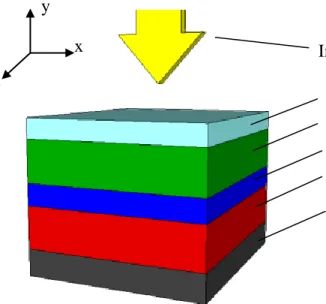
(negative control group) made of
thickness. Also note that this device cross-section is shown upside down here, with the incident light from the top.) ... 67 Figure 5.2: Cross-sectional view of thin-film organic solar structure made of
glass/ITO/PEDOT:PSS/CuPc/PTCBl/BCP/Ag with the top silver grating. (Here LT stands for layer thickness, P indicates the period, and w1 denotes the width of the top silver grating.) In our simulations, the illumination is set to be normal to the device structure and the architecture is assumed to be infinite along the x and z axes. ... 68 Figure 5.3: Cross-sectional view of thin-film organic solar structure made of
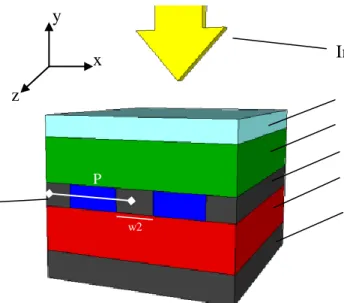
glass/ITO/PEDOT:PSS/CuPc/PTCBl/BCP/Ag with the bottom silver grating. (Here LT stands for layer thickness, P indicates the period, and w2 denotes the width of the bottom silver grating.) In our simulations, the illumination is set to be normal to the device structure and the architecture is assumed to be infinite along the x and z axes... 68 Figure 5.4: Cross-sectional view of thin-film organic solar architecture made of
glass/ITO/PEDOT:PSS/CuPc/PTCBl/BCP/Ag with the volumetric silver gratings (including both the top and bottom metal gratings.)(Here LT stands for layer thickness, P indicates the period of the gratings, and w1 and w2 denote the width of the top and bottom silver grating, respectively.) In our simulations, the illumination is set to be normal to the device structure and the architecture is assumed to be infinite along the x and z axes. ... 69 Figure 5.5: Normalized electric field profiles for the top silver grating, with the
design parameters of P=200 nm (period of the grating), w1=50 nm (width of the top metal grating) under TM-polarized normal-incident illumination at λ=510 nm. The layer thicknesses of the solar cell are LT1=150 nm (ITO), LT2=20 nm (PEDOT:PSS), LT3=11 nm (CuPC), LT5=4 nm (PTCl), and LT5=12 nm (BCP). The incident light is normal to the device structure. Only one unit cell of the repeating grating structure is shown in this electric field profile. ... 71
Figure 5.6: Normalized electric field profiles for the bottom silver grating, with the design parameters of P=200 nm (period of the grating) w2=30 nm (width of the bottom metal grating) under TM-polarized normal-incident illumination at λ=510 nm. The layer thicknesses of the solar cell are LT1=150 nm (ITO), LT2=20 nm (PEDOT:PSS), LT3=11 nm (CuPC), LT5=4 nm (PTCl), and LT5=12 nm (BCP). The incident light is normal to the device structure. Only one unit cell of the repeating grating structure is shown in this electric field profile. ... 72 Figure 5.7: Normalized electric field profiles for the volumetric plasmonic
resonator (including both the top and bottom silver gratings), with the design parameters of P=200 nm (period of the grating), w1=50 nm (width of the top metal grating), and w2=30 nm (width of the bottom metal grating) under TM-polarized normal-incident illumination at λ=510 nm. The layer thicknesses of the solar cell are LT1=150 nm (ITO), LT2=20 nm (PEDOT:PSS), LT3=11 nm (CuPC), LT5=4 nm (PTCl), and LT5=12 nm (BCP). The incident light is normal to the structure. Only one unit cell of the repeating grating structure is shown in this electric field profile. ... 73 Figure 5.8: Absorption spectra of the four solar cell architectures (bare, bottom
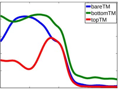
grating, top grating, and volumetric design) with the design parameters of P=200 nm (period of the grating), w1=50 nm (width of the top metal grating), and w2=30 nm (width of the bottom metal grating), under TM-polarized normal-incident illumination. The layer thicknesses of the solar cells are LT1=150 nm (ITO), LT2=20 nm (PEDOT:PSS), LT3=11 nm (CuPC), LT5=4 nm (PTCBl), and LT5=12 nm (BCP). ... 75 Figure 5.9: Absorption spectra of the four solar cell architectures (bare, bottom
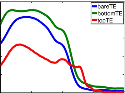
grating, top grating, and volumetric design) with the design parameters of P=200 nm (period of the grating), w1=50 nm (width of the top metal grating), and w2=30 nm (width of the bottom metal grating), under TE-polarized normal-incident illumination. The layer thicknesses of the solar cells are LT1=150 nm (ITO), LT2=20 nm (PEDOT:PSS), LT3=11 nm (CuPC), LT5=4 nm (PTCBl), and LT5=12 nm (BCP). ... 75
Figure 5.10: Overall absorption (ATM+ATE)/2 spectra of the four solar cell
architectures (bare, bottom grating, top grating, and volumetric design) with the design parameters of P=200 nm (period of the grating), w1=50 nm (width of the top metal grating), and w2=30 nm (width of the bottom metal gratings. The layer thicknesses of the solar cells are LT1=150 nm (ITO), LT2=20 nm (PEDOT:PSS), LT3=11 nm (CuPC), LT5=4 nm (PTCBl) and LT5=12 nm (BCP). ... 76 Figure 5.11: AM1.5G solar irradiance spectrum [4]. ... 78 Figure 5.12: Normalized absorptivity map of the bare solar cell for comparison.
These absorption spectra are computed for the parameters of LT1=150 nm, LT2=20 nm, LT3=11 nm, LT4=4 nm and LT5=12 nm... 80 Figure 5.13: Normalized absorptivity map of only the bottom metallic grating
solar cell as a function of the periodicity of the silver grating under TE-polarized light. Here the absorption spectra are computed for the device parameters of w2=30 nm, LT1=150 nm, LT2=20 nm, LT3=11 nm, LT4=4 nm, and LT5=12 nm. ... 80 Figure 5.14: Normalized absorptivity map of only the bottom metallic grating
solar cell as a function of the periodicity of the silver grating under TM-polarized light. Here the absorption spectra are computed for the device parameters of w2=30 nm, LT1=150 nm, LT2=20 nm, LT3=11 nm, LT4=4 nm, and LT5=12 nm. ... 81 Figure 5.15: Normalized absorptivity map of only the top metallic grating solar
cell as a function of the periodicity of the silver grating under TE-polarized light. Here the absorption spectra are computed for the device parameters of w1=50 nm, LT1=150 nm, LT2=20 nm, LT3=11 nm, LT4=4 nm, and LT5=12 nm. ... 81 Figure 5.16: Normalized absorptivity map of only the top metallic grating solar
cell as a function of the periodicity of the silver grating under TM-polarized light. Here the absorption spectra are computed for the device parameters of w1=50 nm, LT1=150 nm, LT2=20 nm, LT3=11 nm, LT4=4 nm, and LT5=12 nm. ... 82
Figure 5.17: Normalized absorptivity map of volumetric metallic gratings solar cell as a function of the periodicity of the silver grating under TE-polarized light. Here the absorption spectra are computed for the device parameters of w1=50 nm, w2=30 nm, LT1=150 nm, LT2=20 nm, LT3=11 nm, LT4=4 nm, and LT5=12 nm. ... 82 Figure 5.18: Normalized absorptivity map of volumetric metallic gratings solar
cell as a function of the periodicity of the silver grating under TM-polarized light. Here the absorption spectra are computed for the device parameters of w1=50 nm, w2=30 nm, LT1=150 nm, LT2=20 nm, LT3=11 nm, LT4=4 nm, and LT5=12 nm. ... 83 Figure 5.19: Normalized absorptivity map of only the top metallic grating solar
cell as a function of the periodicity of the silver grating under TE-polarized light. Here the absorption spectra are computed for the device parameters of w1=60 nm, LT1=150 nm, LT2=20 nm, LT3=11 nm, LT4=4 nm, and LT5=12 nm. ... 83 Figure 5.20: Normalized absorptivity map of only the top metallic grating solar
cell as a function of the periodicity of the silver grating under TM-polarized light. Here the absorption spectra are computed for the device parameters of w1=60 nm, LT1=150 nm, LT2=20 nm, LT3=11 nm, LT4=4 nm, and LT5=12 nm. ... 84 Figure 5.21: Normalized absorptivity map of volumetric metallic gratings solar
cell as a function of the periodicity of the silver grating under TE-polarized light. Here the absorption spectra are computed for the device parameters of w1=60 nm, w2=30 nm, LT1=150 nm, LT2=20 nm, LT3=11 nm, LT4=4 nm, and LT5=12 nm. ... 84 Figure 5.22: Normalized absorptivity map of volumetric metallic gratings solar
cell as a function of the periodicity of the silver grating under TM-polarized light. Here the absorption spectra are computed for the device parameters of w1=60 nm, w2=30 nm, LT1=150 nm, LT2=20 nm, LT3=11 nm, LT4=4 nm, and LT5=12 nm. ... 85
Figure 5.23: Normalized absorptivity map of only the top metallic grating solar cell as a function of the periodicity of the silver grating under TE-polarized light. Here the absorption spectra are computed for the device parameters of w1=40 nm, LT1=150 nm, LT2=20 nm, LT3=11 nm, LT4=4 nm, and LT5=12 nm. ... 85 Figure 5.24: Normalized absorptivity map of only the top metallic grating solar
cell as a function of the periodicity of the silver grating under TM-polarized light. Here the absorption spectra are computed for the device parameters of w1=40 nm, LT1=150 nm, LT2=20 nm, LT3=11 nm, LT4=4 nm, and LT5=12 nm. ... 86 Figure 5.25: Normalized absorptivity map of volumetric metallic gratings solar
cell as a function of the periodicity of the silver grating under TE-polarized light. Here the absorption spectra are computed for the device parameters of w1=40 nm, w2=30 nm, LT1=150 nm, LT2=20 nm, LT3=11 nm, LT4=4 nm, and LT5=12 nm. ... 86 Figure 5.26: Normalized absorptivity map of volumetric metallic gratings solar
cell as a function of the periodicity of the silver grating under TM-polarized light. Here the absorption spectra are computed for the device parameters of w1=40 nm, w2=30 nm, LT1=150 nm, LT2=20 nm, LT3=11 nm, LT4=4 nm, and LT5=12 nm. ... 87
List of Tables
Table 3.1: Confirmed solar cell architectures and their corresponding measured efficiencies under the AM1.5G solar spectrum at 25OC. This table considers the latest and the highest achieved efficiency values considering both organic and inorganic solar cell architectures which is published annually by Green M. et al. This table is taken from “Solar cell efficiency tables (version 35)” published in 2010 [45]. ... 28
Chapter 1
Introduction
Today climate change, also referred to as global warming by some scientists, is considered to be one of the most challenging problems that humankind faces in this century according to some scientific committees [1,2]. It is important to identify the sources of climate change in order to innovate proper solutions to mitigate the causes and negative effects on humankind and on Earth. Nanotechnology, especially nanophotonics, can offer some potential solutions to help combating with climate change from various aspects such as decreasing the global energy power consumption by solid state lighting, reducing environmental and biological pollution by photocatalytic nanomaterials, and producing alternative energy in a renewable, e.g., by photovoltaics.
Photovoltaics is potentially a promising technology for producing electricity possibly on a medium-large scale [3]. In 2008, approximate global electricity production capacity via photovoltaics was 5 GW and by 2015 this production is foresighted to be in order of 20 GW, which is yet a fraction of global electricity demand [4]. Photovoltaics seems to be a good candidate to remedy the energy
problem in the world only if the cost of photovoltaics is reduced or the efficiency of photovoltaics is increased by a factor of 2-5 to be competitive with today’s fossil fuel based energy production [4]. For that, new generation thin film solar cells are designed to feature very thin layers of active (absorbing) materials in the order of tens of nanometers in thickness. Although this approach may decrease the cost of solar cells possibly to reasonable levels, these ultra-thin absorbing layers ruinously suffer from low total optical absorption of incident photons. To address this problem, there has been a great interest in designing plasmonic structures to enhance the total optical absorption in the active layers of these thin-film solar cells [4,5].
Plasmonics is one of the leading research topics of the fascinating field of nanophotonics, which investigates how electromagnetic waves can be confined in metallic architectures in order of or much more smaller than their wavelength, among other things. The interaction between electromagnetic waves and conducting electrons at a metallic interface result in a field localization. This near field enhancement can be benefited in different photonic applications including plasmonic waveguides, nanoscale optical antennas, plasmon-assisted surface-enhanced sensing, plasmonic integrating circuits, plasmonic lasers, metallic apertures for extraordinary transmission, plasmonic optical emitters, materials with negative refractive index, and plasmon-resonance enhanced solar cells [6-9].
Recent research efforts on improving the absorption behavior of organic and inorganic solar cells via exciting plasmonic modes have attracted significant attention all around the world [4,5]. In the literature, generally three ways of enhancing the optical absorption in solar cells are studied: (1) metallic nanoparticles or periodic structures integrated on top of the absorbing material to excite the plasmon modes and couple the incoming light into the thin-film absorbing layer [4,5,10-28,31,32], (2) metallic nanoparticles integrated into the absorbing layer to use them as a sub-wavelength antennas that enhance the
optical absorption with near-field plasmonic field localization [4,29-31,33,37], and (3) metallic periodic structures and random metallic nanoparticles placed on the backcontact surface to use surface plasmon polaritons excited at metal/dielectric interface and enhance the optical absorption with supported surface plasmon polaritons modes at this interface [4,34-36,38-42]. Generally these architecture ideas are based on placing only single resonators at the top, in the middle, or at the bottom of active layers for exciting plasmon modes. Nevertheless, there is a need for innovative design that utilizes the volume of the active layer of the thin-film solar cell and achieves higher enhancement levels beyond the reported values to date.
In this thesis, different than the previous works of our group and others, we propose and demonstrate a new design concept of volumetric plasmonic resonator that relies on the idea of coupling two layers of plasmonic structures embedded in an organic solar cell. For this, here we incorporate one silver grating on the top of the absorbing layer and another at the bottom of the active layer to couple them with each other such that field localization is further increased and extended within the volume of the active material between gratings. In addition to individual plasmonic resonances of these metallic structures, this allows for the vertical interaction in the volumetric resonator. This interaction contributes to further enhancement of total optical absorption in the active layer, beyond the limited photon absorption in non-metallic (bare) organic solar cell. Our results show that this architecture exhibits a substantial absorption enhancement performance particularly under the transverse magnetic (TM) polarized illumination, while the optical absorption is maintained at a similar level under the transverse electric (TE) polarized illumination. As a result, the optical absorption in the active layer is enhanced up to ~67% under AM1.5G (air mass (1.5) global) solar radiation.
Also in this thesis, we study the effect of periodic grating place on top of backcontact in a P3HT:PCBM based solar cell for the first time. In the previous
reports, there are various types of metallic architectures that have been shown to enhance the absorption of solar cell active layers [4,34-36,38-42]. However it is challenging to make plasmonic structures that achieve high enough absorption enhancement under both transverse electromagnetic and transverse magnetic polarizations. Using a silver periodic metallic grating structure in P3HT:PCBM based organic solar cell, we achieve a ~21% performance enhancement under AM1.5G solar radiation compared to the bare device even when the active material is replaced by metallic gratings and no additional active layer is added.
In this thesis work, we proved our proposed concepts computationally and showed our numerical results based on finite-difference time-domain (FDTD) method simulations. The FDTD method is currently the state-of-the-art numerical method for solving Maxwell’s curl equations in time domain on discretized spatial grids [55-56]. This method allows us to use experimentally measured complex dielectric constant of materials in the definition of the materials and simulate designed complex geometries.
This thesis is organized as follows. In Chapter 1, we begin with a brief introduction on plasmonic solar cells and explain our motivation. We discuss the issues of today’s solar cells and plasmonic approaches reported in the literature to overcome this problem. Our proposed solutions are presented, which rely on enhancing the optical absorption of solar cells via plasmonics in new architectures. In Chapter 2, we present the technical background and basic concepts on plasmonics including basics of surface plasmons and basics of localized surface plasmons. We review the plasmonic resonator approaches in the literature for solar cells. Also in this chapter, we make an introduction to the FDTD method and show the basics of numerical simulation in Lumerical Software. In Chapter 3, we introduce the principles of organic photovoltaics including general architecture of organic solar cells, their operation principles and materials commonly used in fabrication of thin-film solar cells. In Chapter 4, we present periodic metal grating placed on top of backcontact in a
P3HT:PCBM based solar cell for enhanced absorption in both polarizations (TE and TM). We present the numerical results of our FDTD simulations. In Chapter 5, we present our new volumetric design concept based on using two coupled plasmonic resonators placed vertically in single organic solar cells. We also present the absorptivity and optimization results of these organic solar cells based on volumetric plasmonic resonators. In Chapter 6, we summarize the proposed plasmonic structures and their proof-of-concept demonstrations based on FDTD modeling.
Chapter 2
Fundamentals of Plasmonics
Plasmonics is a subfield of nanophotonics, which mainly focuses on how electromagnetic field interacts with metals in the order of or smaller than the wavelength. The extraordinary consequences of the interaction between the light and metal are described by the surface plasmon theory [6-9].
In this chapter, we start our discussion with a short history of plasmonics. We then continue with discussing surface plasmons and localized surface plasmons. We also explain the application of plasmonics in photovoltaics and provide a brief description on finite-difference time-domain simulations, which is a useful, simple tool for understanding the effect of plasmonics and a widely used simulation technique in this thesis.
In early times, the technique of coloring stain glasses by very small gold and silver particles was known to Romans. The first application of surface plasmons in the history is the famous Lycurgus Cup (4th century A.D.), shown in Figure 2.1, which changes its color depending on the illumination from inside or
outside. When viewed in reflected light with illumination from outside, for example, in daylight, it appears green. However, when a light is shone into the cup and transmitted through the glass, it appears red. Nowadays it is known that the coloration of the cup is determined by the frequency of surface plasmon resonance in metallic nanoparticles embedded into the glass [9].
Figure 2.1: Lycurgus Cup (4th century A.D.) under different illuminations from outside (left) and inside (right) in British Museum (retrieved from the webpage http://www.britishmuseum.org/explore/highlights/highlight_objects/pe_mla/t/the_lycurgus _cup.aspx).
Some of the first scientific studies on surface plasmons started in the beginning of the twentieth century. Robert W. Wood, an American physician, noticed an inexplicable reflection caused by metallic gratings in 1902. In 1904, Maxwell Garnett worked on understanding the reason behind the observed vivid colors in metal nanoparticle doped glasses using the Drude model that explains the transport properties of electrons in metals derived by Paul Drude. In Maxwell Garnett’s work, the electromagnetic properties of tiny metal spheres were studied using Lord Rayleigh’s approaches. The further understanding on surface
plasmons continued with Gustav Mie’s theory on light scattering properties of spherical particles in 1908 [8,9].
After some years, the research on surface plasmons continued with David Pines by describing the oscillations of free electrons travelling around the metals in 1956. In this work, “plasmons” term was articulated for the first time in science in the description of plasma oscillations in gas discharges. In mid 1950s, the pioneering work of Rufus Ritchie, published in Physics Letters by the title “Plasma losses by fast electrons in thin films”, is the first paper that recognized the surface plasmons in the field of surface science by introducing a theoretical description of these collective oscillations. Following this step, localized plasmons were exhibited by Rufus Ritchie in 1973; by Martin Fleischmann et al. in 1974 and by Martin Moskovits in 1985. The introduction of plasmonics into engineered nanostructure started with Thomas Ebbesen in 1998 with a demonstration of extraordinary light transmission through subwavelength holes, which has subsequently boosted scientific research on plasmonics [8,9]. Today, plasmonics is applied to different photonic device architectures including waveguides, optical data storage devices, biological sensors, and solar cells, typically to improve their device performance beyond the limits [6-9].
2.1 Surface Plasmons
Surface plasmons (SPs) are electromagnetic waves that propagate along the surface of a conductor, usually a noble metal such as Au, Ag, and Al, while evanescently confined in the perpendicular direction. The free charges in the metal make collective oscillations at the metal/dielectric interface due to excitation of incident photons. SPs receive strong interest with the recent advances in technology that has started to allow metals to be shaped and characterized at nanometer scales. Shaping the nanostructures enables us to
control the properties of SPs to disclose new aspects of its usage and open new applications [6-9].
Figure 2.2: Dielectric/metal interface considered in the dispersion relation derivation of surface plasmons. The structure is omitted to be infinite in y direction [7].
The basic theory behind the surface plasmons can be described on a flat metal/dielectric interface, as depicted in Figure 2.2. We know that the interaction between metals and electromagnetic waves can be described by fundamental Maxwell’s equations. However, in plasmonics, and also in our structures, we consider metallic structures in the order of few nanometers. Even when we go down to this small scale, classical Maxwell equations are capable of describing the interaction between metal and electromagnetic waves, since the high density of free carriers results in minute spacings of the electron energy levels compared to thermal excitations of energy kBT at room temperature. All
metal structures described in this thesis fall within the domain of classical Maxwell’s theory. Thus, we start our derivation by stating the Maxwell equations [7]. Basic Maxwell’s equations of macroscopic electromagnetism are given as: (2.1) (2.2) (2.3) (2.4) ε1(ω) ε2
where D is the dielectric displacement, E is the electric field, H is the magnetic field, B is the magnetic induction (or magnetic flux density), is the external
charge, and is the external current density. In this representation, we
represent the external charge and current densities ( ) and the internal charge and current densities ( ) as:
(2.5)
(2.6)
The relations between the four macroscopic fields (D, B, E, H) and the polarization P and magnetization M are given as:
(2.7)
(2.8)
where is the electric permittivity and is the magnetic permeability of vacuum.
To determine the spatial field profile and dispersion of propagating waves, we need explicit expressions for the different field components of E and H. This can be achieved via using the curl equations given in (2.3) and (2.4).
Equation (2.3) can be rewritten as:
(2.9)
where
(2.10)
The explicit expressions for E fields along x, y and z direction lead to: (2.11) (2.12) (2.13)
Similarly, (2.4) can be rewritten as:
(2.14)
(2.15)
The explicit expressions for E fields along x, y and z direction yield:
(2.16) (2.17) (2.18)
For waves propagating in x-direction, setting
, and assuming
homogeneity in the y-direction, setting
, the equations simplify into:
(2.19)
(2.20)
(2.22)
(2.23)
(2.24)
For TM mode, these equations (2.19-2.24) reduce to: (2.25) (2.26)
and the wave equation for TM mode becomes
(2.27)
For TE mode, these equations (2.19-2.24) boil down to:
(2.28)
(2.29)
and the wave equation for TE mode becomes
(2.30)
Now we consider the starting simple planar geometry, given in Figure 2.2, sustaining surface plasmon polaritons, based on a single, flat interface between a nonabsorbing dielectric layer with a real dielectric constant ε2 and a metal layer
with a dielectric function that depends on frequency, ε1(ω). Let us first look at
(2.31) (2.32) (2.33) In dielectric (for z>0), (2.34) (2.35) (2.36)
At the boundary (z=0), Hy and Ex for metal and dielectric must be equal to each
other due to continuity. Thus, the equality yields:
(2.37) (2.38) (2.39) (2.40) (2.41)
This condition must be satisfied for SPs to exist. This condition is satisfied only at the interfaces between materials with opposite signs of the real part of their dielectric permittivites such as metal and dielectric. Surface plasmons are visualized in Figure 2.3 for TM polarized illumination.
Figure 2.3: Visualization of surface plasmons at the metal/dielectric interface: the surface charge oscillations in the transverse magnetic (TM) case, while the magnetic field (H) is in the y-direction and the electric field (E) is normal to the surface [6].
The TM solutions for given in (2.31) and (2.34) must satisfy the wave equation for TM modes given in (2.27), which gives the conditions of,
(2.42)
(2.43)
After solving the Maxwell equations with proper boundary conditions, the resonant interaction between the surface charge oscillation and the light illumination – electromagnetic field – is given as:
(2.44)
where is the dispersion relation of surface plasmons propagating at the metal/dielectric interface and and are the frequency dependent permittivity of the metal and real dielectric permittivity constant of the dielectric medium, respectively. This condition is satisfied for metals because the dielectric function ( ) is both complex and negative. The dispersion relation shown in Figure 2.4
demonstrates that the SP mode always lies beyond the light line; that is, SP mode has a greater momentum (ksp) than a free space photon (k0) of the same
frequency ω. Therefore, there exists a momentum mismatch, which prevents free-space light from directly being coupled into a SP mode. This is the first consequence of the interaction between electromagnetic field and surface charges.
Figure 2.4: Dispersion relation for existing surface plasmons [6].
The second consequence is that the field near dielectric/metal interface decreases exponentially with the distance from the surface (Figure 2.5). The field in the perpendicular direction has evanescent behavior due to nonradiative nature of SPs, which prevents power from propagating away from the surface.
Figure 2.5: The electric field profile at the dielectric/metal interface. δd is the decay length of the field in dielectric medium and δm is the decay length of the field in metal medium [6].
In the literature, three main techniques are used to overcome the momentum mismatch problem. The first approach is to use a prism coupling setup to modify the momentum of the incident light. The second approach uses topological defects on the surface such as subwavelength holes and grids, which provide a convenient way to generate SPs locally. The third approach is based on using a periodic corrugation in the metal, e.g., metal gratings, which constitutes the main idea of our plasmonic resonator design in organic solar cells in this thesis [6].
Previously, we considered TM solution of SPs. Let us now look at TE solutions of surface plasmons. In metal (for z<0), (2.45) (2.46) (2.47)
In dielectric (for z>0), (2.48) (2.49) (2.50)
At the boundary (z=0), Hx and Ey for metal and dielectric must be equal to each
other due to continuity. Thus, the equality leads to:
(2.51)
(2.52)
Since the Re{k1} and Re{k2} is greater than 0, this condition is only satisfied for
the case of A1=0. Thus no surface plasmon mode exists under TE polarization.
Surface plasmons only exist under TM polarized illumination [7].
From solar cell point of view, the surface plasmons are beneficial for efficient light absorption if the absorption of the surface plasmons in the semiconductor is stronger than in the metal (Figure 2.6). When we satisfy this condition, the surface plasmon resonances produce a very strong and stable charge displacement and also light concentration at the dielectric interface. The dielectric layer is made of an absorbing material in our case. Large field increases in the absorbing material contributes to total optical absorption, which is given by:
Figure 2.6: Field profile of light-to-surface plasmon polariton coupling by a grating at a metal/dielectric interface. The metallic film is on the bottom surface of the silica substrate. Light is incident normally from above on the coupling grating [9].
2. 2 Localized Surface Plasmons
We have seen that surface plasmons are propagating electromagnetic waves at the metal and dielectric interface. These are propagating, dispersive electromagnetic waves that occur when the surface plasmon momentum condition is satisfied. Localized surface plasmons, or localized plasmons, are simply non-propagating resonances that occur both in the near-field and inside the conductor due to excitation of the conductor free electrons with the incident electromagnetic wave. As a consequence of curved surfaces and sufficient penetration depth, localized surface plasmon resonances can be formed by direct light illumination, in contrast to propagating surface plasmon resonances. Thus, the localized surface plasmons can be excited under TE and TM illumination [7].
If these resonances – also called as field amplification – occur in the absorbing material, the absorptivity of the active material increases. Localized surface
plasmon based absorption enhancement is observed in solar cell architectures where the metallic plasmonic resonators are placed on top of the absorbing layer. The interaction between the electromagnetic wave and the metal resonator causes great field amplification under the resonating structure, which is mainly an absorbing material. In one of our simulation outputs, it is possible to observe the localized surface plasmons and surface plasmon polaritons due to excitation of plasmon modes in metallic grating structure (Figure 2.7). The field amplification that takes place under the metallic grating is localized in the active material, and as a result, enhancement in absorptivity is observed.
Figure 2.7: Visualization of localized surface plasmons (under the silver grating) and surface plasmons (on the silver grating) under the TM polarized normal-incident illumination at λ=510nm. The incident light is normal to the structure (shown with arrow). Unit cell of the structures is visualized in the electric field profiles.
2.3 Plasmonics for Photovoltaics
The recent research efforts on increasing the optical absorption of organic and inorganic solar cells via exciting plasmonic modes have attracted significant attention all around the world [4,5]. In the literature, generally three ways of enhancing the optical absorption in the solar cells are studied: 1.) metallic nanoparticles or metallic periodic gratings placed on top of absorbing material to
excite the plasmon modes and couple the incoming light into the thin-film absorbing(plasmonic photovoltaics type 1). These nano-metallic structures excite plasmon modes at different wavelengths and are tailored to particular frequencies by engineering the architecture geometry [4,5,10-28,31,32]. 2.) The second method is to integrate metallic nanoparticles into absorbing layer to use them as sub-wavelength antennas, which enhance the optical absorption with near-field plasmonic field increase [4,29-31,33,37] (plasmonic photovoltaics type 2). 3.) Metallic periodic structures and random metallic nanoparticles on the backcontact surface to use surface plasmon polariton excited at metal/dielectric interface and enhance the optical absorption with supported surface plasmon polariton modes at this interface [4,34-36,38-42] (plasmonic photovoltaics type 3). Generally these architecture ideas are based on placing only single layer of resonators at the top, in the middle, or at the bottomof the active layers for exciting plasmon modes.
The first approach relies on the use of random metallic nanoparticles or periodic metallic structures on top of absorbing material as sketched in Figure 2.8. This approach allows solar cell to trap the light in the absorbing layer due to back reflection of the light from the back of metallic structure, besides exciting the plasmon modes in metal/dielectric surface. The frequencies of allowed plasmon modes can be adjusted by engineering the nano-metallic structures including geometry of the metallic structure, periodicity of the architecture, diameter of the metallic nanoparticle and the type of the metal. At some frequencies especially at high frequencies (low wavelengths), covering the absorbing material with a metallic surface may cause a direct reflection of incoming light. However, the excited surface plasmon modes at other frequencies cause extraordinary oscillations in free electrons in the metal, and they consequently generate highly localized electric fields in the dielectric, which is set to be the absorbing material. This high field concentration contributes to absorptivity of solar cell structure since the absorptivity is linearly dependent on the field intensity (field amplitude square). This approach can also be applied to other
type of light trapping devices such as photodetectors [11,15]. In plasmonic photodetectors, matching the surface plasmon resonance frequency of specially engineered metallic geometry at the operating frequency of the detector leads to increased sensitivity of the photodetector because of allowed plasmon mode at the operating frequency.
Figure 2.8: Metallic nanoparticles embedded on top of absorbing material to excite the plasmon modes at metal/dielectric interface (plasmonic photovoltaics type 1) [4].
The second plasmonic design approach is to embed random metallic nanoparticles into the active as shown in Figure 2.9. Here the high near-field concentrations localized around the metal allow for the creation of electron-hole pairs in the absorbing material [4]. Also, if the nanoparticles are close enough to each other, it is possible to take the advantage of metal-to-metal interaction, which causes great field increase in the semiconductor [29]. However, the drawback of this approach is that metallic nanoparticles are mixed with absorbing material and it is thus impossible to engineer the design parameters including the distance between the nanoparticles and location of the nanoparticles due to randomness.
Figure 2.9: Metallic nanoparticles embedded in absorbing material to excite the plasmon modes around the metal nanoparticles (plasmonic photovoltaics type 2) [4].
This second method integrates these metallic nanoparticles into absorbing layer also to employ them as sub-wavelength antennas, which enhance the optical absorption with near-field plasmonic field localization [4].
The last method reported in literature is to metallic periodic structures or metallic nanoparticles on top of the back contact of the solar cell architecture given in Figure 2.10. The surface plasmons excited at the dielectric/metal interface propagates in the plane of absorbing layer and high field concentration enhances the optical absorption in surface plasmon resonance frequencies [4].
Figure 2.10: Metallic periodic structures integrated with the backcontact (plasmonic photovoltaics type 3) [4].
2.4
Finite-Difference
Time-Domain
(FDTD)
method
The FDTD method is presently the state-of-the-art computation approach for solving Maxwell’s curl equations in time domain on discretized spatial grids. This method is first introduced by Kane Yee in 1966. The idea of this method is to solve time dependent Maxwell equations represented in partial differential form by using central-difference approximations to the space and time partial derivatives on a discretized grid. This method has become a popular one for solving electromagnetic problems after progressive advancement in computing technology. Today FDTD method is a widely used technique for understanding the interaction between electromagnetic waves and material structures [55,56]. In this thesis, the numerical simulations that computationally prove our proposed concepts for enhancing the optical absorption in solar cell using new plasmonic architectures are carried out by this method.
FDTD is a time domain solver. However, generally FDTD simulators are used to calculate the electromagnetic fields as a function of frequency (or wavelength). Frequency responses of fields are computed by performing Fourier transforms during the simulation. This allows to obtain complex-valued fields and other derived quantities such as the complex Poynting vector, normalized transmission, and far field projections as a function of frequency (or wavelength).
Figure 2.11: A screenshot from Lumerical software user interface.
We performed our simulations with a commercial FDTD software package, which is developed by Lumerical Solutions Inc., Vancouver, Canada (Figure 2.11). The flow chart of creating a simulation in Lumerical FDTD solver is as follows: 1.) generating the structures and assigning material types to these structures, 2.) creating a simulation region, and 3.) selection of the source and placing the data monitors in simulation region.
The software allows us to shape any kind of composite structures via controlling a CAD tool embedded into software. After creating the structures, the material types need to be assigned with corresponding complex refractive indices as a function of frequency. This method allows us to use experimentally measured complex dielectric constant of materials in the definition of the material. Dispersive materials with tabulated refractive index (n,k) data as a function of wavelength can be assigned by the users. The tabulated refractive indexes are also available for well known materials such as Ag, Au, and Al, and different types of references such as Palik, and Johnson and Christy.
After creating the investigated structure and assigning the material properties, the simulation area limits the region where the simulations will be performed should be set. In this section, assigning proper boundary conditions (BC) of the simulation area is important. Lumerical Solutions package supports a range of boundary conditions including: 1.) perfectly matched layer BC (PML) – this condition allows the PML to strongly absorb outgoing waves from the interior of a computational region without reflecting them back into the interior, 2.) periodic BC – this condition is used in the structures that continue along the infinity with some periodicity in the structure architecture and, 3.) Bloch BC – this condition is used when the structures are periodic, and the EM fields are periodic, except for a phase shift between each period.
Sources make another important component of a simulation. FDTD Solutions support a number of different types of sources such as point dipoles, beams, plane waves, total-field scattered-field (TFSF) sources, guided-mode source for integrated optical components and imported sources for interface with external photonic design softwares.
Chapter 3
Principles of Organic Solar Cells
Today renewable and clean energy production is one of the most important components of the global new energy strategy. Photovoltaics receive great attention among other renewable resources because utilizing the power of the Sun is certainly one of the most viable ways to help to combat the foreseeable climate change. Though common materials used in photovoltaics are inorganic materials, there has also been an increasing effort to develop organic solar cells within the last decades. Organic solar cells are particularly attractive because of their ease of processing, non-toxicity, mechanical flexibility and potential for low cost printing of large areas [43,44,46-48]. Thus, in this thesis, we mainly focus on applying and demonstrating plasmonic resonator structures on these promising devices based on different types of organic solar cell architectures.
The advantages make this class of devices attractive, however their low photon conversion efficiency is one of the main problems to be overcome [45]. The latest achieved efficiency levels with their corresponding solar cell structures are gathered and shown in Table 3.1. The results show that the photon conversion efficiencies of these organic solar cell structures under the AM1.5G solar
radiation are noticeably low compared to inorganic solar cell architectures available today. These efficiency values are not high enough to win the competition against mature inorganic photovoltaics technologies; hence, there is a clear need for developing more efficient organic solar cell architectures by optimizing absorbing materials or cell architectures, or embedding functional nanostructures, e.g., to utilize the advantage of surface plasmon excitations in the case of metal nanopatterns. In this thesis, we concentrate on proposing and computing nanometallic resonators to enhance the optical absorption beyond the photon absorption limits in non-metallic organic thin-film solar cell architectures.
Table 3.1: Confirmed solar cell architectures and their corresponding measured
efficiencies under the AM1.5G solar spectrum at 25OC. This table considers the latest and
the highest achieved efficiency values considering both organic and inorganic solar cell architectures which is published annually by Green M. et al. This table is taken from “Solar cell efficiency tables (version 35)” published in 2010 [45].
In this chapter, we start our discussion with discussing the general operation principles of organic solar cells by constituting a theoretical background of the organic photonic devices. We will overview the materials that are typically used in organic solar cells. In this chapter, we also give further information on the cell

![Figure 2.8: Metallic nanoparticles embedded on top of absorbing material to excite the plasmon modes at metal/dielectric interface (plasmonic photovoltaics type 1) [4]](https://thumb-eu.123doks.com/thumbv2/9libnet/5914060.122597/44.893.343.622.375.603/metallic-nanoparticles-embedded-absorbing-dielectric-interface-plasmonic-photovoltaics.webp)
![Figure 2.9: Metallic nanoparticles embedded in absorbing material to excite the plasmon modes around the metal nanoparticles (plasmonic photovoltaics type 2) [4]](https://thumb-eu.123doks.com/thumbv2/9libnet/5914060.122597/45.893.334.629.199.423/metallic-nanoparticles-embedded-absorbing-material-nanoparticles-plasmonic-photovoltaics.webp)
![Figure 3.5: Chemical structures of examples of hole-conducting materials that work as electron donor: ZnPC, MDMO-PPV, P3HT, and PFB [44]](https://thumb-eu.123doks.com/thumbv2/9libnet/5914060.122597/57.893.295.672.469.861/figure-chemical-structures-examples-conducting-materials-electron-donor.webp)