LOCALIZED PLASMON-COUPLED
SEMICONDUCTOR NANOCRYSTAL
EMITTERS FOR INNOVATIVE
DEVICE APPLICATIONS
A THESIS
SUBMITTED TO THE DEPARTMENT OF ELECTRICAL AND ELECTRONICS ENGINEERING
AND THE INSTITUTE OF ENGINEERING AND SCIENCES OF BILKENT UNIVERSITY
IN PARTIAL FULLFILMENT OF THE REQUIREMENTS FOR THE DEGREE OF
MASTER OF SCIENCE
By
İbrahim Murat Soğancı
August 2007
ii
I certify that I have read this thesis and that in my opinion it is fully adequate, in scope and in quality, as a thesis for the degree of Master of Science.
Assist. Prof. Dr. Hilmi Volkan Demir (Supervisor)
I certify that I have read this thesis and that in my opinion it is fully adequate, in scope and in quality, as a thesis for the degree of Master of Science.
Assist. Prof. Dr. Vakur B. Ertürk
I certify that I have read this thesis and that in my opinion it is fully adequate, in scope and in quality, as a thesis for the degree of Master of Science.
Assist. Prof. Dr. Dönüş Tuncel
Approved for the Institute of Engineering and Sciences:
Prof. Dr. Mehmet B. Baray
iii
ABSTRACT
LOCALIZED PLASMON-COUPLED
SEMICONDUCTOR NANOCRYSTAL EMITTERS
FOR INNOVATIVE DEVICE APPLICATIONS
İbrahim Murat Soğancı
M.S. in Electrical and Electronics Engineering Supervisor: Assist. Prof. Dr. Hilmi Volkan Demir
August 2007
Quantum confinement allows for the development of novel luminescent materials such as colloidal semiconductor quantum dots for a variety of photonic applications spanning from biomedical labeling to white light generation. However, such device applications require efficient photoluminescence. To this end, in this thesis we investigate the spontaneous emission characteristics of semiconductor nanocrystal emitters under different conditions and their enhancement and controlled modification via plasmonic resonance coupling, placing metallic nanoparticles in their proximity, for innovative device applications. We first present our theoretical and experimental work on the optical characterization of nanocyrstals (e.g., CdSe, CdS, and CdSe/ZnS) including absorption/photoluminescence, time-resolved luminescence, and excitation spectra measurements. Here we demonstrate very strong electromodulation (up to 90%) of photoluminescence and absorption of such nanocrystals (nanodots and nanorods) for optical modulator applications. Second, we present our electromagnetic modeling on the optical response of metal nanoparticles using finite-difference-time-domain method. For the first time, using localized plasmons of metal nanoisland films (nano-silver) carefully spectrally and spatially tuned for optimal coupling conditions, we report very significant controlled modifications of nanocrystal emission including the peak
iv
emission wavelength shift (by 14nm), emission linewidth reduction (by 10nm with 22% FWHM reduction), photoluminescence intensity enhancement (15.1- and 21.6-fold compared to the control groups of the same nanocrystals with no plasmonic coupling and those with identical nano-silver but no dielectric spacer in the case of non-radiative energy transfer, respectively), and selectable peaking of surface-state emission at desired wavelengths. Such localized plasmonic engineering of nanocrystal emitters opens new possibilities for our light-emitting and photovoltaic devices.
Keywords: Quantum confinement, quantum dots, nanocrystals, nanorods,
spontaneous emission, photoluminescence, electromodulation, metal nanoparticles, localized plasmons, metal-enhanced luminescence, FDTD.
v
ÖZET
YENİLİKÇİ AYGIT UYGULAMALARI İÇİN
LOKAL PLAZMON KATKILI
YARIİLETKEN NANOKRİSTAL IŞIYICILAR
İbrahim Murat Soğancı
Elektrik ve Elektronik Mühendisliği Bölümü Yüksek Lisans Tez Yöneticisi: Yrd. Doç. Dr. Hilmi Volkan Demir
Ağustos 2007
Kuvantum sınırlandırma, kolloidal yarıiletken kuvantum noktaları gibi ışıyıcı malzemelerin biyomedikal görüntülemeden beyaz ışık üretimine kadar uzanan çeşitli fotonik uygulamalar için kullanılmasını olanaklı kılmaktadır. Sözü edilen aygıt uygulamaları verimli fotoışıma gerektirmektedir. Bu amaçla, bu tez çalışmasında yarıiletken nanokristallerin kendiliğinden ışınsalım özelliklerini değişik koşullarda inceledik ve yenilikçi aygıt uygulamaları için yakınlarına metal nanoparçacıklar yerleştirerek plazmon rezonans etkisiyle artışını ve denetimli değişikliğini sağladık. Öncelikle, nanokristallerin (örneğin CdSe, CdS ve CdSe/ZnS) soğurma/fotoışıma, zaman-çözümlü ışıma ve uyarma tayfı ölçümlerini içeren optik karakterizasyonu üzerine kuramsal ve deneysel çalışmalarımızı sunduk. Optik kipleyici uygulamaları için, nanokristallerde (nano-noktalar ve nano-çubuklar) çok güçlü (% 90’a kadar) fotoışıma ve soğurma elektro-kiplemesi gösterdik. Ardından, zamanda sonlu farklar (FDTD) yöntemiyle metal nanoparçacıkların optik yanıtı üzerine elektromanyetik modellememizi sunduk. İlk defa, metal nano-ada filmlerin (nano-gümüş) lokal plazmonlarını uzaysal ve spektral olarak optimum optik etkileşim için tasarlayıp kullanarak, ışıma doruk dalgaboyu kayması (14 nm), ışıma eğrisi daralması (yarı yükseklikteki tam genişlikte % 22’ye denk gelen 10 nm’lik daralma), fotoışıma şiddet artışı (aynı nanokristallerin plazmonik etkileşim olmadığı ve aynı nanokristaller ile aynı nano-gümüş arasında dielektrik katman olmadığı
vi
durumlara göre sırasıyla 15.1 ve 21.6 kat) ve yüzey ışımasının istenilen dalgaboyunda seçilmiş doruklandırılması gibi nanokristal ışıması ile ilgili çarpıcı değişiklikleri deneysel olarak gerçekleştirdik. Bu tez çalışmasında nanokristallerin bu şekilde lokal plazmon mühendisliği, ışık yayan ve fotovoltaik aygıtlarımız için yeni olanaklar sunmaktadır.
Anahtar sözcükler: Kuvantum sınırlandırma, kuvantum noktaları, nanokristaller,
nano-çubuklar, kendiliğinden ışınsalım, fotoışıma, elektro-kipleme, metal nanoparçacıklar, lokal plazmonlar, metalle artırılan ışıma, zamanda sonlu farklar (FDTD).
vii
Acknowledgements
I would like to express my gratitude to my supervisor, Asst. Prof. Dr. Hilmi Volkan Demir for his supervision and support from the beginning to the end of my master’s study. With his wisdom and personality, he is a model for my academic future.
I would like to thank the members of my thesis committee, Asst. Prof. Dr.Vakur B. Ertürk and Asst. Prof. Dr. Dönüş Tuncel for their useful comments and suggestions.
I would like to thank Prof. Dr. Ekmel Özbay for the facilities at Nanotechnology Research Center. Without those equipments, it would be impossible to accomplish this experimental research work.
I would like to thank our research partner Dr. Sergey Gaponenko at the Institute of Atomic and Molecular Physics of Belarus for providing me their characterization equipments and great hospitality for two weeks.
I would like to thank Evren Mutlugün, Sedat Nizamoğlu, Emre Ünal, Onur Akın, Emre Sarı, Dr. Nihan Kosku Perkgöz, Özgün Akyüz, Sümeyra Tek, İlkem Özge Huyal, Tuncay Özel, Can Uran, Aslı Koç, Gülis Zengin, and Rohat Melik from Demir Group and Bayram Bütün, Turgut Tut, Deniz Çalışkan, Erkin Ülker, Evrim Çolak and Atilla Özgür Çakmak from Özbay Group for their invaluable support.
I would also like to thank my family for making it possible to achieve my goals since my childhood.
Finally, I would like to acknowledge the financial support of TÜBİTAK (Scientific and Technological Research Foundation of Turkey) as a scholarship during my master’s study.
viii
Table of Contents
ACKNOWLEDGEMENTS...VII 1. INTRODUCTION...1 2. SURFACE PLASMONS ...52.1SURFACE PLASMON POLARITONS...5
2.1.1 Physical Explanation ...5
2.1.2 Excitation of Surface Plasmon Polaritons ...7
2.1.3 Field Enhancement ...10
2.2LOCALIZED SURFACE PLASMONS...11
2.2.1 Physical Explanation ...11
2.2.2 Parameters Affecting Resonance Conditions...14
2.2.2.1 Size ... 14
2.2.2.2 Shape ... 15
2.2.2.3 Material ... 15
2.2.2.4 Medium Properties... 16
2.3ELECTROMAGNETIC SIMULATION OF LOCALIZED SURFACE PLASMONS...16
2.3.1 The Finite-Difference Time-Domain Method...16
2.3.2 Implementation...18
2.3.3 Results ...25
3. SEMICONDUCTOR NANOCRYSTALS...35
3.1THEORY...35
3.1.1 Definition and Basics...35
3.1.2 Energy States in Quantum Dots...36
3.1.3 Broadening mechanisms...39
3.2EXPERIMENTAL CHARACTERIZATION...41
3.2.1 Nanocrystal Processing Techniques...41
3.2.2 Optical Absorption and Emission Measurements...42
3.2.3 Electromodulation of Optical Properties of CdSe Nanorod and Nanodot Films ...47
4. LOCALIZED PLASMON-COUPLED EMISSION OF NANOCRYSTALS...53
4.1METAL-ENHANCED LUMINESCENCE...53
4.2METAL NANOSTRUCTURES PREPARATION...57
4.3EXPERIMENTAL DEMONSTRATION OF LOCALIZED PLASMON-COUPLED EMISSION FROM NANOCRYSTALS...63
4.3.1 Plasmon-Coupled Emission of CdSe/ZnS Nanocrystals ...63
4.3.2 Plasmon-Engineered Emission of Surface State-Emitting Nanocrystals ...70
ix
List of Figures
Figure 1. 1 Representative cross section of a core-shell nanocrystal with
surfactants (ligands) at the outermost surface (after [1])... 2 Figure 2.1.1. 1 Surface charges and electric field distribution perpendicular to
the surface. Also, the magnetic field is depicted (after [10]) ... 6 Figure 2.1.1. 2 Comparison of dispersion relations of surface plasmon polariton
modes at a metal-dielectric interface and photons in the same dielectric medium (after [12]). ... 7 Figure 2.1.2. 1 Scattering of electrons in the metal film (a), and the position of
the corresponding wave vector on the surface on the dispersion curve (after [11]). ... 8 Figure 2.1.2. 2 Reflection of light at a metal-dielectric boundary. Medium 1 is
metal and medium 2 is air or vacuum (after [11])... 9 Figure 2.1.2. 3 Comparison of wave vector of light with an angle of incidence of θ0 in free space (1) , in medium 0 (2), with the dispersion relation graph of
surface plasmon polaritons at medium 1-medium 2 interface (after [11]). ……10 Figure 2.2.1. 1 Real and imaginary components of the dielectric constant of
silver plotted as a function of photon energy. The width of the curves represents the amount of experimental error (after [16]). ... 13 Figure 2.3.1. 1 Yee cell ... 18 Figure 2.3.2. 1 Real (a) and imaginary (b) parts of the dielectric permittivity of
silver plotted using Drude model ... 20 Figure 2.3.3. 1 Diagram representing the simulation region... 26 Figure 2.3.3. 2 The comparison of electric field amplitude at the surface of the
nanosphere in longitudinal axis and without the presence of silver nanosphere at the same location when excited at 390 nm free-space
wavelength (the unit of x-axis is seconds and the unit of y-axis is arbitrary). ... 27
x
Figure 2.3.3. 3 The comparison of electric field amplitude at a distance of 0.8 nm from the surface of the silver nanosphere in longitudinal axis and without the silver nanosphere at the same location when excited at 390 nm free-space wavelength (the unit of x-axis is seconds and the unit of y-axis is arbitrary)... 28 Figure 2.3.3. 4 The comparison of electric field amplitude at a distance of 1.6
nm from the surface of the silver nanosphere in longitudinal axis and without the silver nanosphere at the same location when excited at 390 nm free-space wavelength (the unit of x-axis is seconds and the unit of y-axis is arbitrary)... 29 Figure 2.3.3. 5 The comparison of electric field amplitude at the surface of the
silver nanosphere in transverse axis and without the silver nanosphere at the same location when excited at 390 nm free-space wavelength (the unit of x-axis is seconds and the unit of y-axis is arbitrary)... 30 Figure 2.3.3. 6 The comparison of electric field amplitude at a distance of 0.8
nm from the surface of the silver nanosphere in transverse axis and without the silver nanosphere at the same location when excited at 390 nm free-space wavelength (the unit of x-axis is seconds and the unit of y-axis is arbitrary)... 31 Figure 2.3.3. 7 The comparison of electric field amplitude at a distance of 1.6
nm from the surface of the silver nanosphere in transverse axis and without the silver nanosphere at the same location when excited at 390 nm free-space wavelength (the unit of x-axis is seconds and the unit of y-axis is arbitrary)... 32 Figure 2.3.3. 8 Enhanced electromagnetic field intensity distribution with
respect to distance from the surface with a 1/r6-dependence (the unit of x-axis is nm and the unit of y-x-axis is arbitrary). ... 33 Figure 2.3.3. 9 Spectral distribution of electric field amplitude at the surface of
silver nanocylinder (the unit of x-axis is nm and the unit of y-axis is
arbitrary)... 34 Figure 3.1.3. 1 Evolution of the optical absorption spectrum of semiconductor
nanocrystals with full-width at half-maximum enlarging with increasing size distribution in the ensemble (after [32])... 40 Figure 3.2.2. 1 Absorption and photoluminescence spectra of CdSe/ZnS
core-shell nanocrystals with diameters of 2.1 nm (a), 2.7 nm (b), and 5.3 nm (c). ... 44
xi
Figure 3.2.2. 2 Photoluminescence excitation and photoluminescence spectra of CdSe/ZnS nanocrystals with peak emission wavelength of 623 nm (a) and 585 nm (b). ... 45 Figure 3.2.2. 3 Time-resolved photoluminescence of CdSe/Zns core-shell
nanocrystals with emission wavelengths of 585 nm (a) and 620 nm (b). .. 47 Figure 3.2.3. 1 Photoluminescence spectra of CdSe nanorods film under
different applied voltages. Inset shows the integrated PL intensity vs. the applied electric field. ... 49 Figure 3.2.3. 2 Differential PL (a) and normalized differential PL (b) spectra of
CdSe nanorods vs. applied electric field. ... 50 Figure 3.2.3. 3 Optical density of CdSe nanodots for different electric field
values... 51 Figure 3.2.3. 4 Photoluminescence of CdSe nanodots for different electric field
values... 52 Figure 3.2.3. 5 Differential photoluminescence spectra of CdSe nanodots under
different applied electric fields... 52 Figure 4.1. 1 Distance dependence of the three mechanisms (quenching,
increased field, and increased rate) caused by metal-luminophore
interaction (after [43]) ... 55 Figure 4.2. 1 SEM images of our silver nanoisland films: (a) 20 nm mass
thickness, not annealed, (b) 20 nm mass thickness, annealed at 300 ºC for 10 min., (c) 6 nm mass thickness, annealed at 150ºC for 1 min., and (d) 2 nm mass thickness, annealed at 150ºC for 2 min. ... 58 Figure 4.2. 2 Optical absorption spectra of silver nanoislands with mass
thickness of 4 nm annealed at 300ºC for 20 min, nano-silver (2 nm) at 150 ºC for 2 min, nano-silver (6 nm) at 150ºC for 2 min, and nano-silver (6 nm) at 150 ºC for 2 min covered with 10 nm thick SixOy film. ... 59
Figure 4.2. 3 Optical absorption spectrum of a gold island film with a mass thickness of 4 nm annealed at 300 ºC for 10 minutes. ... 61 Figure 4.2. 4 Optical absorption spectrum of a silver-gold alloy metal island
film. The mass thicknesses of silver and gold are 2 nm, the annealing temperature is 300 ºC, and the annealing duration is 10 minutes. ... 62
xii
Figure 4.3.1. 1 Schematic view of the two types of samples prepared: a 10 nm thick silicon oxide film between metal island films and nanocrystals (a), and nanocrystals directly on metal island film (b). ... 65 Figure 4.3.1. 2 Optical absorption spectra of Ag (20 nm) annealed at 300 ºC for
10 min and that also covered with 10 nm-thick SixOy along with the
photoluminescence spectrum of CdSe/ZnS nanocrystals... 66 Figure 4.3.1. 3 Photoluminescence peak intensity of CdSe/ZnS nanocrystals
with silver (20 nm) and a dielectric spacer (10 nm silicon oxide) between them is 15.1 times larger than that of the same CdSe/ZnS nanocrystals alone and 21.6 times stronger than that of the same CdSe/ZnS nanocrystals with identical silver nanoislands (20 nm) but no dielectric spacer. ... 67 Figure 4.3.1. 4 Photoluminescence peak wavelength of CdSe/ZnS
nanocrystals+SixOy+nanoAg (506 nm) is shifted by 14 nm with respect to
CdSe/ZnS nanocrystals alone (492 nm) due to plasmonic resonance coupling. Their FWHM linewidth is also narrowed by 10 nm due to the plasmon coupling. ... 68 Figure 4.3.1. 5 Electroluminescence spectrum of the LED with CdSe/ZnS
core-shell nanocrystals close to silver island films (a), and of the same sample (with no metal structures) isolated from any plasmon coupling (b)... 69 Figure 4.3.2. 1 Photoluminescence spectrum of surface state emitting CdS
nanocrystals. ... 70 Figure 4.3.2. 2 Photoluminescence spectrum of surface state emitting
nanocrystals without the influence of plasmons compared with those of the same material close to silver and gold nanoislands with the plasmonic coupling. ... 71
xiii
List of Tables
Table 4.2. 1Average silver nanoisland diameter for different deposition
conditions ... 59 Table 4.2. 2Localized plasmon resonance wavelengths of metal island films
1
Chapter 1
Introduction
In recent years, significant scientific research has been performed on semiconductor and metal nanoparticles especially because of their interesting optical characteristics, which are not observed in bulk materials. Carrier and photon confinement in such semiconductor and metal nanoparticles under certain circumstances (i.e., resonance conditions) is the reason of these different optical characteristics. As a result of these peculiar optical properties, the use of such nanoparticles in photonic device applications is promising to obtain better performances by modifying currently available devices and to invent new ones with novel functionality.
Nanocrystals have crystalline structure (periodic stacking of atoms), but consist of nanometer-size clusters, with diameters comparable to the exciton Bohr radius and the de Broglie electron wavelength, and are distinctly separated from each other. Among the examples of such semiconductor nanocrystals are those from II-VI, III-V and VI-VI Groups. Colloidal nanocrystals are chemically synthesized, and their sizes and formations are controlled through chemical reaction parameters. Figure 1.1 presents a representative cross-section of a core-shell nanocrystal. The electron confinement in nanocrystals, i.e., the quantum confinement, leads to discretization of energy levels, making major changes in the energy spectrum of electronic excitation and probability of optical transitions (thus the optical absorption and emission spectra). Therefore, the bandgap energy of the nanocrystals is size-dependent and both their absorption edge and peak emission wavelength can be tuned within a certain spectral range
2
conveniently by controlling their crystal size. Both optical absorption and emission processes are efficient in these quantum-confined structures. For example, the luminescence quantum efficiency of II-VI Group nanocrystals may be very high, in some cases as high as 80 % at room temperature [2]. Because of all these interesting optical properties, nanocrystals have great potential to be used in new optical and optoelectronic devices. The ability to fine-tune their optical properties using size effect is the most important advantage of nanocrystals, making it possible to increase the performance of existing devices, and even facilitate to implement new functions. Our research activities are focused on the quantum mechanical and electromagnetic mechanisms to engineer the optical processes taking place in nanocrystals. To this end, in this thesis we investigate the optical properties of different nanocrystals (made of CdSe, CdS and CdSe/ZnS) modified in a controlled manner under different conditions (e.g., under electric field, with plasmonic resonance coupling) for innovative device applications.
Figure 1. 1 Representative cross section of a core-shell nanocrystal with surfactants (ligands) at the outermost surface (after [1]).
Surface plasmons are the collective oscillations of conduction band electrons at the surfaces of metal films or in metal nanoparticles. The technical term of “propagating surface plasmons” (and sometimes only “surface plasmons”) is used for plasmons on continuous metal surfaces and the term of “localized
3
surface plasmons” (and “particle plasmons”) is used for plasmons in metal nanoparticles and metal nanostructures. Plasmons can be optically excited if the optical frequency and wave vector of the incident photons match those of the plasmons. At specific resonance frequencies, plasmon modes generate very large amplitudes of electron oscillations. Around the resonance frequencies, the local electromagnetic field in the vicinity of the electron oscillations may be very high, which we prove by solving Maxwell’s equations using the finite-difference time-domain method. The interplay between plasmons and photons make very interesting applications possible, including surface-enhanced Raman scattering [3], enhanced nonlinear optical processes [4], plasmon-enhanced two-photon absorption [5], and metal-plasmon-enhanced fluorescence [6]. Similar interactions between plasmonic metal nanoparticles and nanocrystal emitters also exhibit such interesting results, and in this thesis we investigate the localized plasmonic engineering of the nanocrystal photoemission experimentally. Considering the spatial and spectral conditions of strong plasmon-nanocrystal interactions, we design, fabricate and characterize metallic nanostructures. These results prove to be promising, with significant enhancement in the luminescence intensity, shift in the peak emission wavelength and narrowing in the emission linewidth. This opens new opportunities for device applications as also suggested and experimented.
The organization of this thesis is as follows: In Chapter 2 we introduce surface plasmons. In this chapter, the physical explanation of surface plasmons and localized plasmons is provided; their optical excitation methods, the spatial and spectral distribution of the electromagnetic fields in their vicinity and the effects of particle and structure properties on resonance conditions are explained. Here we also provide our electromagnetic simulations of the field distribution around metal nanospheres under different excitation conditions. Chapter 3 focuses on semiconductor nanocrystals. This chapter includes theoretical explanation of the optical properties of semiconductor nanocrystals, description of experimental techniques for nanocrystal film preparation, and their optical characterization under different conditions (e.g., under electric
4
field). In Chapter 4, plasmon-material interactions are included. The physical interactions leading to metal-enhanced fluorescence are discussed; our experimental method of producing metal nanostructures is presented with the systematic study of fabrication conditions; our design for the optimization of metal-nanocrystal interactions is presented; significant modification in the emission characteristics of nanocrystals in our fabricated structures are demonstrated; and our device applications of such plasmon-coupled nanocrystal emitters are introduced with experiment results.
5
Chapter 2
Surface Plasmons
Surface plasmon is a quantum of collective oscillations of conduction band electrons in metals [7]. The oscillations of these negatively charged carriers are accompanied with electromagnetic fields. The boundary conditions of the electromagnetic fields accompanying electron oscillations on metal surfaces and in metal nanoparticles are different. This leads to different physical solutions to these two situations known as surface plasmons for on-surface oscillations and localized plasmons for in-nanoparticle oscillations.
2.1 Surface Plasmon Polaritons
2.1.1 Physical Explanation
The existence of surface plasmon oscillations on metal-dielectric boundaries was demonstrated by Powell and Swan using electron energy-loss experiments [8]. These oscillations on metal-dielectric boundaries bring together electromagnetic fields in close proximity to the surface. Such electromagnetic excitations bounded to the free charges on conductor surfaces are named as polaritons [9], and the whole phenomenon including the surface plasma waves and the accompanying fields is called as surface plasmon polaritons. Figure 2.1.1.1
6
displays the electrons at a metal-dielectric interface and the spatial distribution of the accompanying fields.
Figure 2.1.1. 1 Surface charges and electric field distribution perpendicular to the surface. Also, the magnetic field is depicted (after [10])
Assuming that there is no dependence in the y-axis, the electric field distribution of a surface polariton propagating on the x direction as in Figure 2.1.1.1 is as follows:
E= E0exp[i(kxx±kzz−ωt)] (2.1.1.1) where kz is imaginary and kx is real (and the sign of kzz term is positive if z>0, and negative if z<0). This means that the electric field amplitude decays exponentionally in the z-axis and and behaves as a propagating wave in the x-axis.
The dispersion relation of surface plasmon polaritons is given by the following equation [11]: 2 / 1 ⎟⎟ ⎠ ⎞ ⎜⎜ ⎝ ⎛ + = d m d m x c k ε ε ε ε ω (2.1.1.2)
where ω is the oscillation frequency, εm is the permittivity of the metal, and εd is the permittivity of the dielectric at the interface. The dispersion relation is demonstrated in Figure 2.1.1.2. Also plotted in the same figure is the dispersion relation of a photon propagating in the adjacent dielectric. Close to the surface plasmon resonance frequency, the wave vector of the surface plasmon polaritons is larger than that of the photon at equal frequencies. This makes it impossible to match the wave vector and the frequency of polaritons and those of the photons at
7
the same time, which means that surface plasmon polaritons cannot be excited by electromagnetic radiation from the dielectric, and electromagnetic radiation cannot be created in the dielectric by the surface plasmon modes on the metal surface without using additional techniques.
Figure 2.1.1. 2 Comparison of dispersion relations of surface plasmon polariton modes at a metal-dielectric interface and photons in the same dielectric medium (after [12]).
2.1.2 Excitation of Surface Plasmon Polaritons
Surface plasmon polaritons can be excited by electrons or by light. Electrons penetrating to the metal surface are scattered and leave some momentum and energy for the electrons on the metal surface. The projection of the momentum on the propagation plane of the surface plasmons determines the wave vector of the excited modes, which is defined as kx in the assumption of two dimensions as above. This wave vector also determines the energy through the dispersion relation. Figure 2.1.2.1 presents the scattering of electrons in the metal and displays the position of wave vector on the dispersion curve. The theory of excitation of surface plasmon polaritons by electrons has been verified, finding out the dispersion relation plotted in Figure 2.1.1.2 experimentally [11].8
Figure 2.1.2. 1 Scattering of electrons in the metal film (a), and the position of the corresponding wave vector on the surface on the dispersion curve (after [11]).
The excitation of surface plasmon polaritons by light requires additional techniques because at a given photon energy the wave vector of surface plasmon polaritons is larger than that of the incident photons as discussed above. One method of achieving this on smooth surfaces is the use of a grating coupler. The light incident on a grating coupler with a grating constant a, at an angle θ0 may have wave vectors
(
ω/c)
sinθ0±vg of its component in the surface, where v is an integer andg=2π /a. Therefore, the equationkSP =
(
ω/c)
sinθ0±vg (2.1.2.1)
gives the surface plasmon wave vector. The reverse is also valid, in which surface plasmons with the aforementioned wave vectors couple to electromagnetic radiation through a grating coupler.
9
The second method to excite surface plasmon polaritons on smooth surfaces by light relies on the attenuated total reflection (ATR) coupling. After the reflection of light from a metal surface covered with a dielectric medium withε0 >1, its momentum is equal to (hv/c) ε0 because the speed of light isc/ ε0 in the dielectric. For an angle of incidence of θ0,
ω ε0sinθ0
c
kx = (2.1.2.2)
is the projection on the surface. Considering the case in Figure 2.1.2.2, the incident light has the wave number projection as in equation 2.1.2.2, and the dispersion relation of surface plasmon polariton modes at the boundary between medium 1 and medium 2 is equal to
2 / 1 1⎟⎟⎠ ⎞ ⎜⎜ ⎝ ⎛ + = m m x c k ε ε ω (2.1.2.3)
if medium 2 is air or vacuum. Figure 2.1.2.3 compares the functions in equations 2.1.2.2 and 2.1.2.3, and shows that there is a region of intersection in the graph, which makes it possible to excite surface plasmon modes in the air-metal boundary using total internal reflection from a medium with higher refractive index [11].
Figure 2.1.2. 2 Reflection of light at a metal-dielectric boundary. Medium 1 is metal and medium 2 is air or vacuum (after [11]).
10
Figure 2.1.2. 3 Comparison of wave vector of light with an angle of incidence of θ0 in free
space (1) , in medium 0 (2), with the dispersion relation graph of surface plasmon polaritons at medium 1-medium 2 interface (after [11]).
2.1.3 Field Enhancement
Since the surface plasmon polariton fields decay perpendicular to the metal-dielectric surface, they are bounded in the near field. Therefore, the field is significantly enhanced at this region. The field enhancement factor at a smooth surface is calculated from
[
(
)
]
m s s m m m d SP Elight z E ε ε ε ε ε ε ε 1 Re 1 Re Im Re 2 ) 0 ( 2 2 1/2 + − − = = (2.1.3.1)where εs is the permittivity of the prism used to illuminate the metal [12]. The enhancement can be higher than two orders of magnitude for a 60 nm-thick silver film exposed to white light [12].
11
2.2 Localized Surface Plasmons
Localized surface plasmons are the quanta of collective oscillations of electrons spatially confined in metal nanoparticles. Their characteristics are quite different from the surface plasmons on smooth surfaces.
2.2.1 Physical Explanation
The response of metal spheres to externally applied electromagnetic radiation can be solved analytically using Maxwell’s equations. Mie solved this electrodynamic problem completely in 1908 [13]. However, quasi-static approximations also yield reasonably correct results especially for diameters smaller than 30 nm, and they are very helpful to create an intuition on the reader. Therefore, we explain the theory of localized surface plasmon using the quasi-static approximation here.
At optical frequencies, the penetration depth of electromagnetic waves is around 30 nm for gold and silver. As the size of the metal nanoparticle is on the order of penetration depth, the electromagnetic fields can penetrate. This causes electric field formation in the particle. As a result, the conduction band electrons shift collectively with respect to the positive charges in the structure. The collection of the opposite charges at the opposite sides of the particle builds up restoring forces [10]. The restoring forces cause an oscillation of the electrons in the particle. Four factors determine the oscillation frequency: the density and effective mass of the electrons, the shape and size of the charge distribution [14]. The density and effective mass of electrons are material parameters. Metals with high density of electrons have stronger oscillations because of larger polarizability. If the frequency of the exciting electric field is equal to the oscillation frequency of the electrons, even a small excitation brings together very strong oscillations. On the resonance condition, the metal nanoparticle becomes an oscillating dipole, and very high local electric fields are induced in
12
the incident polarization axis around this dipole [14]. Quasi-static approximation gives the electric field around the metal nanoparticle excited with an E-field polarized in the x-direction with the following equation [14]
(
)
⎥ ⎦ ⎤ ⎢ ⎣ ⎡ − + + − = xx yy zz r x r x E x E Eout ˆ ˆ 3 ˆ ˆ ˆ 5 3 0 0 α (2.2.1.1)where α is the polarizability of the metal particle and E0 is the amplitude of the incident electric field. The first term on the right hand side is the incident field and the second term on the right hand side is the induced dipole field. From this equation, the induced dipole field has 1/r3 dependence over distance from the center of the particle.
The excited plasmons dampen either in a nonradiative way or by radiating electromagnetic waves. Nonradiative decay is caused by scattering with lattice ions, phonons, the other electrons, surface of the particle, impurities, etc. Nonradiative decay is the dissipation of energy as heat, and contributes to the absorption of the exciting field. Radiative decay occurs as scattering of electromagnetic waves [10]. Both absorption and scattering of the metal nanoparticle are very high around the resonance wavelength, creating a peak at the extinction spectrum. The extinction peak also means local field peak because the electromagnetic field around the particles is linearly proportional to the absorption [15].
Mie theory, neglecting higher order modes, gives the extinction cross section of spherical metal nanparticles as follows [16]
( )
( )
[
]
( )
2 2 2 1 2 2 / 3 2 2 9 ω ε ε ω ε ω ωε ε σ + + = m m ext V c (2.2.1.2)where V is the volume of the particle, ω is the frequency of radiation, εm is the dielectric constant of the surrounding medium, and εmetal =ε1+iε2. To consider the effect of size differences, size-dependent dielectric constants are used. If ε2 is small, which is usually the case in our frequency range of interest,
13
the plasmonic resonance is observed in the extinction cross-section for the case when:
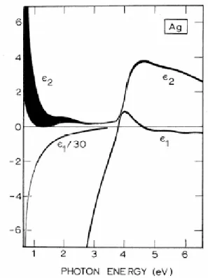
ε1(w)=−2εm (2.2.1.3) This is an important result because it helps us estimate the localized surface plasmon resonance wavelength of metal nanospheres by checking the dispersion relation graphs of the relevant metals. As an example, the dielectric constant of silver as a function of photon energy is displayed in Figure 2.2.1.1 [17]. From this graph, the resonance photon energy for silver nanospheres is expected to be around 3.4 eV.
Figure 2.2.1. 1 Real and imaginary components of the dielectric constant of silver plotted as a function of photon energy. The width of the curves represents the amount of experimental error (after [17]).
The quasi-static approximation is valid especially for particles with diameters smaller than 30 nm. However, if the diameter of the particle is larger, the quadrupole and octopole modes also become important. In the quadrupole mode, half of the electron cloud moves parallel to the applied field, and the other half
14
antiparallel to it [14]. For large nanoparticles, a superposition of all modes are observable in the extinction cross section spectrum, and the quasi-static approximation explained above does not yield good enough solutions to the excitation of higher order modes in larger particles, if the size of the particle is comparable to the wavelength of excitation, inhomogeneous polarization becomes valid [16].
2.2.2 Parameters Affecting Resonance Conditions
The type of the metal, the shape and size of the nanoparticle and the environment determine the localized plasmon resonance wavelength together. Let us investigate the effects of all factors on the resonance conditions:
2.2.2.1 Size
The parameters effecting the lifetime of localized plasmon resonance depend on the size. As particle size increases, the effect of radiation damping increases, which causes red-shift and broadening of the plasmon resonance for larger particles [18,19]. The mean free path of electrons in gold is about 50 nm and the electron-phonon collision time is 35 fs. For very small particles collisions with the particle surface become important. Therefore, particle size determines the damping constant [16]. In both extremes, the quality of resonance decreases because the mentioned decay mechanisms become dominant. Therefore, there is an optimum size of metal nanoparticles for better resonance behavior. The proportion of absorption and scattering in the extinction of resonant nanoparticles also depends on the size. As the radiative damping becomes dominant for larger sizes, the scattering is dominant over absorption in larger
15
nanoparticles [20]. If the particle diameter is greater than 100 nm, extinction is almost 100 % due to scattering [21].
2.2.2.2 Shape
While for small metallic nanospheres only one resonance (the dipole resonance) is valid, for other geometries multiple resonances may be observed. For example, two resonances are observed in triangle structures [22]. For ellipsoids, the resonance wavelength depends on the polarization of the field. If the polarization is in the long axis, the resonance wavelength is longer compared to the polarization in the short axis. The resonance red-shifts if the aspect ratio of the ellipsoid increases. If one dimension of the particle is within 20 nm, the localized plasmon peak shifts to longer wavelengths dramatically [23]. The particle shape has more influence on the resonance wavelength than the size. In the regions of high surface curvature, the enhancement of the local field is higher because of the lightning rod effect [24]. Therefore, nanoparticles with complex shapes including corners yield higher local field enhancement. For example, silver particles in the shape of triangular prisms cause much higher fields than cylinders [23].
2.2.2.3 Material
Metals with higher electron density are better materials for localized plasmon resonance. For this reason, gold and silver are the materials used the most frequently for resonance plasmon resonance applications. The relation given in equation (2.2.1.3) causes the resonance wavelengths of different metals to be different. The dielectric permittivity as a function of wavelength changes from metal to metal and the wavelength at which it satisfies equation (2.2.1.3) also
16
changes. As an example, for equal particle size and shape and environmental conditions, gold has longer resonance wavelengths than silver.
2.2.2.4 Medium Properties
Again from equation (2.2.1.3), the dielectric constant of the medium influences the resonance wavelength. The higher the dielectric constant of the medium, the red-shifted the plasmon resonance is. Only the properties of surrounding media close enough to the metal particle can significantly affect the resonance conditions. This distance is around 15 nm. Also, if there are other metal nanoparticles in the environment, the distribution of the electric field, and even resonance wavelength are influenced. Between particles very close to each other, field intensities much higher than those near single particles are observed. However, independent of particle size and shape, for gaps sizes larger than 1 nm, the high intensities rapidly decay. As two particles get close to each other, red-shift is observed in the resonance. The particles can be assumed to be isolated for gap sizes larger than the particle size. If the metal nanoparticles are on metal films, surface plasmon polaritons become an efficient channel for the localized plasmon polaritons to decay, causing significant changes in the resonance conditions [12].
2.3 Electromagnetic simulation of localized surface
plasmons
2.3.1 The Finite-Difference Time-Domain Method
To simulate the response of metal nanoparticles to externally applied electromagnetic radiation, we solve Maxwell’s equations using the finite-difference time-domain method. The finite-finite-difference time-domain method17
depends on the central difference approximations. Time and space are divided into grids and the derivatives in time and spatial domain are expressed as the changes in the function around a specific grid.
(, , ) (, , 1/2) (, , 1/2) O[( z)2] z F F z F n k j i n k j i n k j i + ∆ ∆ = ∂ ∂ + − − (2.3.1.1) As given in equation 2.3.1.1, the derivative of the function with respect to z is calculated from the difference of the following and previous grid values divided by the grid size. The second term on the right hand side is the second order error term arising from the discretization, and it is ignored in the calculations. The curl equations from Maxwell’s equations,
Faraday’s Law: t H ∂ ∂ − = Ε × ∇ r r . µ (2.3.1.2-a) Ampere’s Law: J t E H r r r + ∂ ∂ = × ∇ ε. (2.3.1.2-b)
Gauss’ Law for Electric field: ∇ D.r = ρ (2.3.1.2-c) Gauss’ Law for Magnetic field: ∇ B.r=0 (2.3.1.2-d)
are written with all components of the electric and magnetic field vectors, and are discretized using central difference approximations. The electric and magnetic field components are located on a Yee cell as presented in Figure 2.3.1.1.
18
Figure 2.3.1. 1 Yee cell
Uniaxial perfectly matched layers (UPML) are used as the boundary conditions. Perfectly matched layers are used to prevent artificial reflection from the boundaries of the computational domain. For more detailed description of the finite-difference time-domain method and uniaxial perfectly matched layers, the reader is suggested to consult [25,26].
2.3.2 Implementation
Since metals are involved in our electromagnetic problem, we have to take into consideration the effects of dispersion. Drude model is convenient for silver at optical frequencies, with results compatible with the experimental results. The general equation for Drude model is as follows
Γ + − = ∞ ω ω ω ε ω ε j p r 2 2 ) ( (2.3.2.1)
where ε∞ is the dielectric permittivity at infinite frequency, ωp is the plasma frequency and Γ is the relaxation rate of the electrons. For silver, the
19
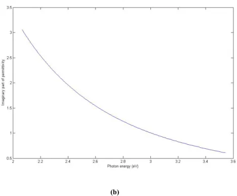
parametersε∞ =8.926, ωp =11.585eV, and Γ=0.203eV give results similar to the experimental ones in the 350 nm-450 nm range [27]. Figure 2.3.2.1 presents the real and imaginary parts of the dielectric permittivity of silver as a function of photon energy calculated using those parameters in the Drude model. These plots are close to the graph in Figure 2.2.1.1 in our wavelength region of interest.
The wavelength-dependent dielectric constant in the finite-difference time-domain method is introduced in the constitutive relation:
D =ε0εrE (2.3.2.2)
20
(b)
Figure 2.3.2. 1 Real (a) and imaginary (b) parts of the dielectric permittivity of silver plotted using Drude model
Substituting equation 2.3.2.1 in equation 2.3.2.2 gives the relationship between
Dand E vectors: E j j D p 0 2 2 2 ) ( ε ω ω ω ωε ω ε ω Γ + − Γ + = ∞ ∞ (2.3.2.3)
Since the finite-difference time-domain method uses time-domain analysis, we have to convert equation 2.3.2.3 from frequency-domain to time-domain. After inverse-Fourier transform is taken,
E E t E t D t D t p 0 2 0 2 2 0 2 2 ε ω ε ε ε ε + ∂ ∂ Γ + ∂ ∂ = ∂ ∂ Γ + ∂ ∂ ∞ ∞ (2.3.2.4)
is derived as the differential equation relating D and E vectors. Equation 2.3.2.4 is used in the finite-difference time-domain calculations to include
21
frequency-dependent dielectric constant of silver. This method is called the “auxiliary differential equation approach” and has been proved to be successful for simulation of dispersive media [28].
The following equations are derived to solve the electromagnetic problems in time domain in the media including dispersive metals, using the auxiliary differential equation approach and uniaxial perfectly matched layers at the boundaries: ⎟⎟ ⎟ ⎟ ⎠ ⎞ ⎜⎜ ⎜ ⎜ ⎝ ⎛ ∆ − − ∆ − × ⎟⎟ ⎟ ⎟ ⎟ ⎠ ⎞ ⎜⎜ ⎜ ⎜ ⎜ ⎝ ⎛ + ∆ + ⎟⎟ ⎟ ⎟ ⎟ ⎠ ⎞ ⎜⎜ ⎜ ⎜ ⎜ ⎝ ⎛ + ∆ − ∆ = − + + + − + + + − + + + z H H y H H j t j P j t j j t j P n k j i y n k j i y n k j i z n k j i z y y n k j i x y y y y n k j i x 2 / 1 , , 2 / 1 2 / 1 , , 2 / 1 , 2 / 1 , 2 / 1 , 2 / 1 , 2 / 1 0 2 / 1 , , 2 / 1 0 0 2 / 1 , , 2 / 1 2 ) ( ) ( 1 2 ) ( ) ( 2 ) ( ) ( ε σ κ ε σ κ ε σ κ (2.3.2.5) ⎟ ⎟ ⎟ ⎠ ⎞ ⎜ ⎜ ⎜ ⎝ ⎛ ∆ − − ∆ − × ⎟ ⎟ ⎟ ⎟ ⎠ ⎞ ⎜ ⎜ ⎜ ⎜ ⎝ ⎛ + ∆ + ⎟ ⎟ ⎟ ⎟ ⎠ ⎞ ⎜ ⎜ ⎜ ⎜ ⎝ ⎛ + ∆ − ∆ = + − + + − + + + − + + + x H H z H H k t k P k t k k t k P n k j i z n k j i z n k j i x n k j i x z z n k j i y z z z z n k j i y , 2 / 1 , 2 / 1 , 2 / 1 , 2 / 1 2 / 1 , 2 / 1 , 2 / 1 , 2 / 1 , 0 2 / 1 , 2 / 1 , 0 0 2 / 1 , 2 / 1 , 2 ) ( ) ( 1 2 ) ( ) ( 2 ) ( ) ( ε σ κ ε σ κ ε σ κ (2.3.2.6) ⎟⎟ ⎟ ⎟ ⎠ ⎞ ⎜⎜ ⎜ ⎜ ⎝ ⎛ ∆ − − ∆ − × ⎟ ⎟ ⎟ ⎟ ⎠ ⎞ ⎜ ⎜ ⎜ ⎜ ⎝ ⎛ + ∆ + ⎟ ⎟ ⎟ ⎟ ⎠ ⎞ ⎜ ⎜ ⎜ ⎜ ⎝ ⎛ + ∆ − ∆ = + − + + + − + + − + + + y H H x H H i t i P i t i i t i P n k j i x n k j i x n k j i y n k j i y x x n k j i z x x x x n k j i z 2 / 1 , 2 / 1 , 2 / 1 , 2 / 1 , 2 / 1 , , 2 / 1 2 / 1 , , 2 / 1 0 2 / 1 2 / 1 , , 0 0 2 / 1 2 / 1 , , 2 ) ( ) ( 1 2 ) ( ) ( 2 ) ( ) ( ε σ κ ε σ κ ε σ κ
22 (2.3.2.7) ⎥ ⎥ ⎥ ⎥ ⎥ ⎥ ⎥ ⎥ ⎥ ⎥ ⎥ ⎥ ⎥ ⎥ ⎦ ⎤ ⎢ ⎢ ⎢ ⎢ ⎢ ⎢ ⎢ ⎢ ⎢ ⎢ ⎢ ⎢ ⎢ ⎢ ⎣ ⎡ ⎟ ⎟ ⎠ ⎞ ⎜ ⎜ ⎝ ⎛ ∆ Γ − ∆ + ∆ − ⎟ ⎟ ⎠ ⎞ ⎜ ⎜ ⎝ ⎛ ∆ Γ + ∆ + ⎟ ⎟ ⎠ ⎞ ⎜ ⎜ ⎝ ⎛ + ∆ Γ − ∆ − ⎟ ⎟ ⎠ ⎞ ⎜ ⎜ ⎝ ⎛ − ∆ × + ∆ Γ + ∆ = = = + − ∞ ∞ − ∞ ∞ ∞ + 2 / 3 , , 2 2 / 1 , , 2 2 / 1 , , 2 2 / 3 , , 2 2 2 / 1 , , 2 2 2 2 2 / 1 , , 2 ) ( 1 ) ( 2 2 ) ( 1 4 2 ) ( 2 ) ( 2 4 2 ) ( 1 n i z y x n i z y x n i z y x n i z y x p n i z y x p p n i z y x P t t P t P t t D w t t D w t w t t D ε ε ε ε ε (2.3.2.8) ⎥ ⎥ ⎦ ⎤ ⎢ ⎢ ⎣ ⎡ ⎟⎟ ⎠ ⎞ ⎜⎜ ⎝ ⎛ − ∆ − ⎟⎟ ⎠ ⎞ ⎜⎜ ⎝ ⎛ + ∆ × ⎥ ⎥ ⎥ ⎥ ⎥ ⎦ ⎤ ⎢ ⎢ ⎢ ⎢ ⎢ ⎣ ⎡ ⎟⎟ ⎠ ⎞ ⎜⎜ ⎝ ⎛ + ∆ + ⎟ ⎟ ⎟ ⎟ ⎠ ⎞ ⎜ ⎜ ⎜ ⎜ ⎝ ⎛ ∆ + ∆ − = − + + + − + + + 2 / 1 , , 2 / 1 0 2 / 1 , , 2 / 1 0 0 0 2 / 1 , , 2 / 1 0 0 2 / 1 , , 2 / 1 2 ) ( ) ( 2 ) ( ) ( 2 ) ( ) ( 1 2 ) ( ) ( 2 ) ( ) ( n k j i x x x n k j i x x x z z n k j i x z z z z n k j i x D t i i D t i i t k k E t k k t k k E ε σ κ ε σ κ ε ε σ κ ε σ κ ε σ κ (2.3.2.9) ⎥ ⎥ ⎦ ⎤ ⎢ ⎢ ⎣ ⎡ ⎟⎟ ⎠ ⎞ ⎜⎜ ⎝ ⎛ ∆ − − ⎟⎟ ⎠ ⎞ ⎜⎜ ⎝ ⎛ ∆ + × ⎥ ⎥ ⎥ ⎥ ⎥ ⎦ ⎤ ⎢ ⎢ ⎢ ⎢ ⎢ ⎣ ⎡ ⎟⎟ ⎠ ⎞ ⎜⎜ ⎝ ⎛ + ∆ + ⎟ ⎟ ⎟ ⎟ ⎠ ⎞ ⎜ ⎜ ⎜ ⎜ ⎝ ⎛ ∆ + ∆ − = − + + + − + + + 2 / 1 , 2 / 1 , 0 2 / 1 , 2 / 1 , 0 0 0 2 / 1 , 2 / 1 , 0 0 2 / 1 , 2 / 1 , 2 ) ( ) ( 2 ) ( ) ( 2 ) ( ) ( 1 2 ) ( ) ( 2 ) ( ) ( n k j i y y y n k j i y y y x x n k j i y x x x x n k j i y D t j j D t j j t i i E t i i t i i E ε σ κ ε σ κ ε ε σ κ ε σ κ ε σ κ (2.3.2.10)
23 ⎥ ⎥ ⎦ ⎤ ⎢ ⎢ ⎣ ⎡ ⎟⎟ ⎠ ⎞ ⎜⎜ ⎝ ⎛ − ∆ − ⎟⎟ ⎠ ⎞ ⎜⎜ ⎝ ⎛ + ∆ × ⎥ ⎥ ⎥ ⎥ ⎥ ⎦ ⎤ ⎢ ⎢ ⎢ ⎢ ⎢ ⎣ ⎡ ⎟⎟ ⎠ ⎞ ⎜⎜ ⎝ ⎛ ∆ + + ⎟⎟ ⎟ ⎟ ⎟ ⎠ ⎞ ⎜⎜ ⎜ ⎜ ⎜ ⎝ ⎛ ∆ + ∆ − = − + + + − + + + 2 / 1 2 / 1 , , 0 2 / 1 2 / 1 , , 0 0 0 2 / 1 2 / 1 , , 0 0 2 / 1 2 / 1 , , 2 ) ( ) ( 2 ) ( ) ( 2 ) ( ) ( 1 2 ) ( ) ( 2 ) ( ) ( n k j i z z z n k j i z z z y y n k j i z y y y y n k j i z D t k k D t k k t j j E t j j t j j E ε σ κ ε σ κ ε ε σ κ ε σ κ ε σ κ (2.3.2.11) ⎥ ⎥ ⎥ ⎦ ⎤ ⎢ ⎢ ⎢ ⎣ ⎡ ∆ − − ∆ − × ∆ + ∆ + ∆ + ∆ − = + − + − − + z E E y E E t j j t B j t j j t j B n k j i y n k j i y n k j i z n k j i z y y n k j i x y y y y n k j i x 2 / 1 , , 2 / 1 , , , 2 / 1 , , 2 / 1 , 0 0 2 / 1 , , 0 0 2 / 1 , , 2 ( ) ( ) 2 ) ( ) ( 2 ) ( ) ( 2 σ κ ε ε σ κ ε σ κ ε (2.3.2.12) ⎥ ⎥ ⎥ ⎦ ⎤ ⎢ ⎢ ⎢ ⎣ ⎡ ∆ − − ∆ − × ∆ + ∆ + ∆ + ∆ − = + − + − − + x E E z E E t k k t B k t k k t k B n k j i z n k j i z n k j i x n k j i x z z n k j i y z z z z n k j i y , , 2 / 1 , , 2 / 1 2 / 1 , , 2 / 1 , , 0 0 2 / 1 , , 0 0 2 / 1 , , 2 ( ) ( ) 2 ) ( ) ( 2 ) ( ) ( 2 σ κ ε ε σ κ ε σ κ ε (2.3.2.13) ⎥ ⎥ ⎥ ⎦ ⎤ ⎢ ⎢ ⎢ ⎣ ⎡ ∆ − − ∆ − × ∆ + ∆ + ∆ + ∆ − = + − + − − + y E E x E E t i i t B i t i i t i B n k j i x n k j i x n k j i y n k j i y x x n k j i z x x x x n k j i z , 2 / 1 , , 2 / 1 , , , 2 / 1 , , 2 / 1 0 0 2 / 1 , , 0 0 2 / 1 , , 2 () () 2 ) ( ) ( 2 ) ( ) ( 2 σ κ ε ε σ κ ε σ κ ε (2.3.2.14)
(
)
(
)
, 1,/2 0 0 0 2 / 1 , , 0 0 0 2 / 1 , , 0 0 2 / 1 , , ) ( ) ( 2 ) ( ) ( 2 ) ( ) ( 2 ) ( ) ( 2 ) ( ) ( 2 ) ( ) ( 2 = + − + ∆ + ∆ + − + ∆ + ∆ + + ∆ + ∆ − = n k j i x z z r x x n k j i x z z r x x n k j i x z z z z n k j i x B k t k i t i B k t k i t i H k t k k t k H σ κ ε µ µ σ κ ε σ κ ε µ µ σ κ ε σ κ ε σ κ ε (2.3.2.15)24
(
)
0(
0)
, 1,/2 0 2 / 1 , , 0 0 0 2 / 1 , , 0 0 2 / 1 , , ) ( ) ( 2 ) ( ) ( 2 ) ( ) ( 2 ) ( ) ( 2 ) ( ) ( 2 ) ( ) ( 2 = + − + ∆ + ∆ + − + ∆ + ∆ + + ∆ + ∆ − = n k j i y x x r y y n k j i y x x r y y n k j i y x x x x n k j i y B i t i j t j B i t i j t j H i t i i t i H σ κ ε µ µ σ κ ε σ κ ε µ µ σ κ ε σ κ ε σ κ ε (2.3.2.16)(
)
(
)
, 1,/2 0 0 0 2 / 1 , , 0 0 0 2 / 1 , , 0 0 2 / 1 , , ) ( ) ( 2 ) ( ) ( 2 ) ( ) ( 2 ) ( ) ( 2 ) ( ) ( 2 ) ( ) ( 2 = + − + ∆ + ∆ + − + ∆ + ∆ + + ∆ + ∆ − = n k j i z y y r z z n k j i z y y r z z n k j i z y y y y n k j i z B j t j k t k B j t j k t k H j t j j t j H σ κ ε µ µ σ κ ε σ κ ε µ µ σ κ ε σ κ ε σ κ ε (2.3.2.17)Equations 2.3.2.5-2.3.2.11 are used to derive the electric field and equations 2.3.2.12-2.3.2.17 are used to derive the magnetic field. These calculations are updated in every time step (and the previous values of the variables are not kept to use the memory efficiently). In the equations, each electric and magnetic field component is written with its location indicated by i, j and k, and the time step
indicated by n. To make the expressions clear: i+1/2 is ∆x2 further from i in
the x-direction, where x∆ is the grid size in the x-axis. The positions in y and z axes are written similarly. In time domain, n+1/2 is 2∆ later than n, where ∆ is the time grid size. κx, κy, κz, σx, σyand σzare the UPML parameters. Inside the working region, κx =κy =κz =1 and σx =σy =σz =0. In the UPML region at the boundaries,
(
)
m x x dx⎟ ⎠ ⎞ ⎜ ⎝ ⎛ − + =1 κ max 1 κ (2.3.2.18-a)(
)
m y y dy⎟ ⎠ ⎞ ⎜ ⎝ ⎛ − + =1 κ max 1 κ (2.3.2.18-b)(
)
m z z =1+ κ max−1⎜⎝⎛dz⎟⎠⎞ κ (2.3.2.18-c)25
where d is the UPML thickness, the typical values of κmaxare around 7, and m
has a value between 3 and 4.
m x x dx⎟ ⎠ ⎞ ⎜ ⎝ ⎛ =σ max σ (2.3.2.19-a) m y y =σ max⎜⎝⎛dy⎟⎠⎞ σ (2.3.2.19-b) m z z dz⎟ ⎠ ⎞ ⎜ ⎝ ⎛ =σ max σ (2.3.2.19 -c) where x m r x = × π +ε ∆ σ 150 1 1 . 1 max (2.3.2.20-a) y m r y = × π +ε ∆ σ 150 1 1 . 1 max (2.3.2.20 -b) z m r z = × π +ε ∆ σ 150 1 1 . 1 max (2.3.2.20 -c)
where εr is the dielectric constant of the medium in the working region.
2.3.3 Results
We investigate the electric field distribution around the silver nanoparticle with different excitation types. Both two-dimensional and three-dimensional problems are solved. The silver particle we use in the simulations is a nanosphere in the case of three dimensions, and it is a nanocylinder with infinite height in the case of two dimensions. The simulation area is indicated in the diagram in Figure 2.3.3.1. The excitation is p-polarized from the region shown as the source in the figure. The refractive index of the medium is selected as 1.5
26
because in most cases the metal nanospheres are dispersed in poly(methyl methacrylate) (PMMA), which has a refractive index of 1.496 [29].
Figure 2.3.3. 1 Diagram representing the simulation region
Figures 2.3.3.2-2.3.3.4 display the comparison of electric field amplitudes at different distances from the surface of a 10 nm-diameter silver nanocylinder with the electric field at the same locations without the existence of the nanosphere in time domain.
27
Figure 2.3.3. 2 The comparison of electric field amplitude at the surface of the nanosphere in longitudinal axis and without the presence of silver nanosphere at the same location when excited at 390 nm free-space wavelength (the unit of x-axis is seconds and the unit of y-axis is arbitrary).
In Figure 2.3.3.2, the location is at the surface of the nanosphere, whereas the distance to the surface is 0.8 nm in Figure 2.3.3.3 and 1.6 nm in Figure 2.3.3.4. The locations are behind the silver nanosphere (in longitudinal direction) when excited with a continuous wave at 390 nm free-space wavelength. The simulations are undertaken in two dimensions with TE polarization. Figures 2.3.3.5-2.3.3.7 are also the comparisons of the electric field amplitudes at 0 nm, 0.8 nm, and 1.6 nm from the surface of the nanosphere in the transverse axis with respect to the incident wave for the same excitation conditions. These figures prove that large amounts of field enhancement is possible very close to
28
the surface of the nanosphere, and it decays very rapidly in a few nanometers. Also, the enhanced field at the transverse axis is larger than that in the longitudinal axis.
Figure 2.3.3. 3 The comparison of electric field amplitude at a distance of 0.8 nm from the surface of the silver nanosphere in longitudinal axis and without the silver nanosphere at the same location when excited at 390 nm free-space wavelength (the unit of x-axis is seconds and the unit of y-axis is arbitrary).
29
Figure 2.3.3. 4 The comparison of electric field amplitude at a distance of 1.6 nm from the surface of the silver nanosphere in longitudinal axis and without the silver nanosphere at the same location when excited at 390 nm free-space wavelength (the unit of x-axis is seconds and the unit of y-axis is arbitrary).
30
Figure 2.3.3. 5 The comparison of electric field amplitude at the surface of the silver nanosphere in transverse axis and without the silver nanosphere at the same location when excited at 390 nm free-space wavelength (the unit of x-axis is seconds and the unit of y-axis is arbitrary).
31
Figure 2.3.3. 6 The comparison of electric field amplitude at a distance of 0.8 nm from the surface of the silver nanosphere in transverse axis and without the silver nanosphere at the same location when excited at 390 nm free-space wavelength (the unit of x-axis is seconds and the unit of y-axis is arbitrary).
32
Figure 2.3.3. 7 The comparison of electric field amplitude at a distance of 1.6 nm from the surface of the silver nanosphere in transverse axis and without the silver nanosphere at the same location when excited at 390 nm free-space wavelength (the unit of x-axis is seconds and the unit of y-axis is arbitrary).
We also plot the 1/r6 dependence over the distance in Figure 2.3.3.8. This is the expected dependence because the intensity of enhanced electromagnetic field around a metal ellipsoid is proportional to 1/r6 [15], where r is the distance from the surface.
33
Figure 2.3.3. 8 Enhanced electromagnetic field intensity distribution with respect to
distance from the surface with a 1/r6-dependence (the unit of x-axis is nm and the unit of
y-axis is arbitrary).
Additionally, we excite the nanocylinder with a beam, which is Gaussian in time in order to investigate the spectral response. The full-width at half-maximum of the beam is 50 fs. The medium is considered as free space. We make simulations with and without the silver nanocylinder and take the Fourier transform of the electric field amplitude in both cases. Figure 2.3.3.9 plots the spectral distribution of the electric field amplitude at the surface of the silver nanocylinder with a 10 nm diameter. The resonance around 340 nm free-space wavelength is clearly visible. This resonance wavelength is slightly shorter than the reported value in the literature, which is 370 nm [22]. The possible reason might be the different Drude model parameters used for silver. However, this
34
graph proves that a local field enhancement is observed around the resonance wavelength of silver nanoparticles.
Figure 2.3.3. 9 Spectral distribution of electric field amplitude at the surface of silver nanocylinder (the unit of x-axis is nm and the unit of y-axis is arbitrary).
35
Chapter 3
Semiconductor Nanocrystals
3.1 Theory
3.1.1 Definition and Basics
Nanocrystals are aggregates of a few hundred to tens of thousands of atoms that combine into a crystalline form of matter known as a cluster. The size of these crystallites ranges from one to tens of nanometers. Within this range of sizes, nanocrystals are larger than molecules, but still much smaller than bulk materials. What makes nanocrystals different from other quantum-confined structures, i.e., quantum wells and quantum wires is the fact that quantum wells and quantum wires have translational symmetry in one or two dimensions, but in nanocrystals translational symmetry is totally broken because there are only a finite number of electrons and holes within the same crystal. As a result, the concepts of electron-hole gas and quasi-momentum cannot be applied to nanocrystals. Also, the finite number of electrons in nanocrystals causes a variety of photoinduced phenomena such as persistent and permanent photophysical and photochemical phenomena, which are known in atomic and molecular physics, but are not applicable to solids. Another point which makes nanocrystals different is their fabrication techniques. Nanocrystals are fabricated using techniques also used in glass technology and colloidal chemistry [30].
36
3.1.2 Energy States in Quantum Dots
In theoretical analysis, nanocrystals are assumed to be a tiny piece of a crystal structure with a spherical or cubic shape, which is known as a quantum dot. In fact, such perfectly spherical or cubic species do not exist in reality. However, this assumption is very useful to understand the physics of nanocrystals by using simplified models and the basic effects coming from three-dimensional spatial confinement. Therefore, particle-in-a-box problem is solved for a simple analysis here. At smaller sizes, quantum chemical approach is used, in which the number of atoms is taken into account instead of the size.
Effective mass approximation is used in the analysis of nanocrystals. According to this approximation, electrons (and holes) are assumed to have the same effective mass as in the ideal infinite crystal of the same stoichiometry. In this approach, we treat the crystallite as a macroscopic crystal with respect to the lattice properties, but consider it as a quantum dot for quasiparticles. The simplest model to analyze nanocrystals is the spherical potential box with infinite potential barriers and with electrons and holes considered to have isotropic effective masses. This problem can be investigated for two different cases of the weak confinement regime and the strong confinement regime. The weak confinement regime is considered when the dot radius a is small, but still a few times larger than the exciton Bohr radius, aB. To give an idea, the exciton Bohr radius is 4.9 nm for CdSe, 2.8 nm for CdS, and 3.8 nm for ZnSe [31]. The exciton center-of-mass motion has quantization in this case. The dispersion law of an exciton in a crystal is as follows:
M K n R E K En g y 2 ) ( 2 2 2 * h + − = (3.1.2.1)
where K is the magnitude of the exciton wave vector, Eg is the bandgap energy of the crystal structure, Ry is the exciton Rydberg energy, n are quantum
37
numbers, and M is the exciton mass calculated from the effective electron mass and the effective hole mass as in equation 3.1.2.2.
M =m*e+m*h (3.1.2.2) In equation 3.1.2.1, the second term on the right hand side represents the Coulomb interaction between the electron and the hole, and the third term comes from the kinetic energy of the exciton. For the case of a nanocrystal, the kinetic energy term in this equation has to be modified because the kinetic energy of an exciton in a quantum dot is discrete. The discrete values can be calculated by solving the particle in a spherical box problem. With the change in the kinetic energy term, equation 3.1.2.1 becomes:
2 2 22 * 2Ma n R E Enml = g − y +h χml (3.1.2.3)
where a is the quantum dot radius, χml are the roots of the Bessel function coming from the center-of-mass motion in a spherical box with infinite external potential barriers. l is the orbital number, determining the angular momentum, and m is the magnetic number, which determines the angular momentum component parallel to the z axis. Since photon absorption can create excitons with zero angular momentum only, the absorption spectrum is derived from the equation above, but with the case that l is equal to zero:
2 2 22 2 * 2Ma m n R E Enm = g − y + h π (3.1.2.4) Equation 3.1.2.4 describes the energy levels for optical transitions in the weak confinement regime [30].
In the strong confinement regime, the dot radius a is much smaller than the exciton Bohr radius, aB. If we assume that the confined electron and hole are both free and model the nanocrystal as a spherical box in an infinite potential wall [32]:
![Figure 1. 1 Representative cross section of a core-shell nanocrystal with surfactants (ligands) at the outermost surface (after [1])](https://thumb-eu.123doks.com/thumbv2/9libnet/5864414.120633/15.918.357.621.625.890/figure-representative-section-nanocrystal-surfactants-ligands-outermost-surface.webp)

![Figure 2.1.1. 2 Comparison of dispersion relations of surface plasmon polariton modes at a metal-dielectric interface and photons in the same dielectric medium (after [12])](https://thumb-eu.123doks.com/thumbv2/9libnet/5864414.120633/20.918.292.673.316.574/figure-comparison-dispersion-relations-polariton-dielectric-interface-dielectric.webp)
![Figure 2.1.2. 1 Scattering of electrons in the metal film (a), and the position of the corresponding wave vector on the surface on the dispersion curve (after [11])](https://thumb-eu.123doks.com/thumbv2/9libnet/5864414.120633/21.918.332.643.175.623/figure-scattering-electrons-position-corresponding-vector-surface-dispersion.webp)
![Figure 2.1.2. 2 Reflection of light at a metal-dielectric boundary. Medium 1 is metal and medium 2 is air or vacuum (after [11])](https://thumb-eu.123doks.com/thumbv2/9libnet/5864414.120633/22.918.324.635.788.1031/figure-reflection-light-dielectric-boundary-medium-medium-vacuum.webp)
![Figure 2.1.2. 3 Comparison of wave vector of light with an angle of incidence of θ 0 in free space (1) , in medium 0 (2), with the dispersion relation graph of surface plasmon polaritons at medium 1-medium 2 interface (after [11])](https://thumb-eu.123doks.com/thumbv2/9libnet/5864414.120633/23.918.330.645.180.528/figure-comparison-incidence-dispersion-relation-surface-polaritons-interface.webp)