POLİTEKNİK DERGİSİ
JOURNAL of POLYTECHNIC
ISSN: 1302-0900 (PRINT), ISSN: 2147-9429 (ONLINE)
URL: http://www.politeknik.gazi.edu.tr/index.php/PLT/index
Analyzing the InGaN LED structures for white
LED applications
Beyaz Led uygulamaları için InGaN LED yapıların
analizi
Yazar(lar) (Author(s)): İlknur KARS DURUKAN, Mustafa Kemal ÖZTÜRK, Süleyman ÖZÇELİK,
Ekmel ÖZBAY
Bu makaleye şu şekilde atıfta bulunabilirsiniz: Kars Durukan İ., Öztürk M, K., Özçelik S., and Özbay E.,
“Analyzing the InGaN LED structures for white LED applications”, Politeknik Dergisi, 20(3): 531-536,
(2017).
To cite this article: Kars Durukan İ., Öztürk M, K., Özçelik S., and Özbay E., “Analyzing the InGaN LED
structures for white LED applications”, Journal of Polytechnic, 20(3): 531-536, (2017).
Erişim linki (To link to this article):
http://www.politeknik.gazi.edu.tr/index.php/PLT/issue/archive
Analyzing The InGaN LED Structures for White LED
Applications
İlknur KARS DURUKAN1*, Mustafa Kemal ÖZTÜRK1,2, Süleyman ÖZÇELİK1,2,Ekmel ÖZBAY3
1Gazi University, Faculty of Sciences,Department of Physics, Ankara 2Photonics Research Center, Gazi University, Ankara, Turkey
3Department of Physics, Bilkent University, Bilkent, Ankara
(Received : 20.08.2016 ; Accepted : 03.11.2016)
ABSTRACT
In this paper, blue-light InGaN/GaN light-emitting diodes were deposited on sapphire substrate by the Metal Organic Chemical Vapor Deposition (MOCVD) to investigate the properties of blue LEDs with various well thickness having different indium composition. Structural properties of LEDs was studied by high-resolution X-ray diffraction (HRXRD), Photoluminescence (PL) and ultraviole (UV). Our aim is to increase the quality of the LED structure by taking advantage of the mosaic structure calculations. The use of LED in commercial areas has increased. But, there are great difficulties in preventing defects. Lateral and vertical crystal size, dislocations, tilt and twist properties are investigated with HR-XRD device by Vegard and William hall semi-experimental methods. While dislocation value of the first sample is lower than first sample with less indium content ration, stress value of first sample is higher than second sample. In addition, The twist angle of first sample is lower. This shows that while the structure is crystallized, the tension is much greater, which is an interesting result. This is due to the mismatch when the diode is cooled to lower temperatures than the growth temperature.
Keywords: InGaN/GaN, MOCVD, HRXRD, PL, UV.
Beyaz Led Uygulamaları için InGaN LED Yapıların
Analizi
ÖZ
Bu makalede, farklı indiyum kompozisyonu ve farklı kuyu kalınlıklarına sahip mavi LED'lerin özelliklerini araştırmak için mavi ışıklı InGaN / GaN ışık yayan diyotlar (LED) safir alttaş üzerine Metal Organik Kimyasal Buhar Biriktirme (MOCVD) yöntemi ile biriktirildi. Mavi LED yapının yapısal özellikleri X ışını kırınımı (XRD), Fotolüminesans (PL) ve Ultraviyole (UV) cihazları ile çalışıldı. Amacımız mozaik yapı hesaplamalarından yararlanarak LED yapısının kalitesini arttırmaktır. Ticari alanlarda LED kullanımı artmıştır. Ancak, kusurların önlenmesinde büyük zorluklar bulunmaktadır. Yanal ve dikey kristal boyutu, kusurlar, eğilme ve burkulma özellikleri, HR-XRD cihazı ile Vegard ve William Hall yarı deneysel yöntemleriyle incelendi. In oranı daha düşük olan birinci örneğin kusur değeri ikinci örnekten daha düşükken, stress değeri daha yüksektir. Buna ek olarak, birinci numunenin burkulma açısı daha düşüktür. Bu, yapının kristalleşmesine rağmen gerilmenin çok daha büyük olduğunu gösteriyor ve bu ilginç bir sonuçtur. Bunun nedeni, LED yapının, büyüme sıcaklığından daha düşük sıcaklıklara soğutulduğunda yapıdaki uyuşmazlıktan kaynaklanmaktadır.
Anahtar Kelimeler: InGaN/GaN, MOCVD, HRXRD, PL, UV.
1. INTRODUCTION
The development of white-light light-emitting diode (LED) has become an important issue for lighting application. Especially, InGaN/GaN-based LED is expected to be an high efficient, ,long lifetime, reliable, cost-effective for the applications to the color display and lighting [1, 2]. Recently, commercial white LED production, phosphors are used for converting UV or blue photons, generated by a single-color InGaN/GaN-based LED, into longer-wavelength lights for color mixing. However, the use of phosphors brings many disadvantages of the Stokes-wave energy loss, low reliability, short lifetime and patent control [1,3,4].
Therefore; The development of phosphor-free white-light LEDs has become an important trend [5-7]. In the light of these developments, different device schemes has been suggested. Since the band gap of InGaN can cover up to the near-infrared range, using InGaN/GaN quantum wells (QWs) of different indium contents and/or thicknesses for emitting lights of various colors to mix into white-light can be obtained. By controlling the width of the QW, different piezoelectric field can be led to different emission wavelengths [6]. However, when most of the carriers are injected to produce the screening effect, the strong QCSE (quantum-confined Stark effect) in a QW of a large well width will ocur. In this case, a significant shift in blue wavelength is observed [8]. In previous studies, InGaN/GaN QWs of different indium contents have been reported [5,9]. QCSE screening effect are still not fully resolved. So, different device schemes
*Corresponding Author e-mail:[email protected]
İlknur KARS DURUKAN, Mustafa Kemal ÖZTÜRK, Süleyman ÖZÇELİK, Ekmel ÖZBAY / Journal of Polytechnic, 2017; 20 (3) : 531-536
must be investigated in detail. Obtained results can provide useful information which is very important for the best quality optoelectronic and other optical devices based on InGaN/GaN-based LEDs.
In this study, two different LED samples with InGaN/GaN multiple QW were grown. This paper is organized as follows. InGaN/GaN LED MQW structures were grown by MOCVD on c-oriented (001) sapphire substrate. The surface morphology of the samples and mosaic nature of the epitaxial layers were examined using nondestructive HRXRD. The mosaic structure parameters were obtained and discussed as depending on the In ratio and width of the QW. The optical characteristics of the InGaN/GaN LED structures were investigated by PL measurement. The transmission of the InGaN/GaN LED structures were investigated by UV analysis. Mosaic defects affect both optical and electrical properties of the structure. In our work, optical behavior of LED was investigated in terms of these mosaic defects. An aim of this study is to analyze stress and structural defects in LED structures in terms of mosaic calculations.
2. EXPERIMENTAL CONDITIONS
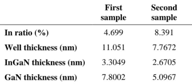
LED MQW structures with 30 nm thick nucleation AlN / GaN layer were grown by MOCVD on c-oriented (001) sapphire substrate (Figure 1). During growth, reactor pressure was fixed at 200 mbar. Before growthing MQWstructure, 700 nm thick AlN / GaN buffer layer produced and then 250 nm thick n-type GaN: Si layer was grown at 1090 ° C. The sample contains 2.2 nm active InxGa1-xN layer which has five periods. The active layer was grown at 710 ° C on the 15.7 nm GaN. Cap layer was covered with 193.6-nm thick layer p-type GaN: Mg at 1030 ° C. Furthermore, the p-type AlN was used for the block type layer. Thickness period of first sample and second sample was 11.1051 nm and 7.7672 nm, respectively. Also; In ratio of first sample and second sample was 4.699 % and 8.391 %. These calculations are calculated in the XRAY data analysis program (LEPTOS) based on the vegard law.
The structural properties and defect analysis of the samples were characterized by the high-resolution X-ray diffraction (XRD) technique using a Bruker D8 system, delivering a CuK1 line. PL measurements were taken by using the JobinYvon Florong-550 PL system with a 50-mW He-Cd laser (λ= 325 nm) as excitation light source at room temperature. The UV–vis optical transmission spectra of the InGaN led structures was measured using a lambda 2S Perkin Elmer UV–vis spectrometer at room temperature.
Layer Matter Thickness (Å) p – Cap layer GaN 2400
InGaN GaN n+ contact GaN Buffer AlN/GaN Nucleation AlN/GaN Substrate Safir
Figure 1. General layer structure of LEDs
3. RESULTS AND DISCUSSION
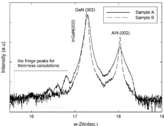
Fig 2 shows the intensity curve for w-2. The solid lines and dashed lines show the first and second samples, respectively. In both samples, the GaN (002) peak is observed at 17.291 and 17.270, respectively. AlN (002) appears on the right side of the GaN (002) peak around 19. In addition, the active layer InGaN is on the left of the GaN (002) peak and it is shouldered with GaN peak. Also, the peaks called fringe peaks and represent the quantum well structure related in thickness and these peaks are shown within square frame.
As the well thickness and the In ratio change, the spacing of the fringe peaks changes. In Figure 2, the peak separation in second sample is greater in the first sample. So the indium ratio is higher while the thickness value is smaller. Plane quality and defects properties of hexagonal structure were obtained with full width at half maximum (FWHM) values of the peaks obtained by w-2 scan. The InxGa1-xN layer can be represented by the GaN layer and The active layer is highly dependent on the structural properties of the GaN layer. Therefore, the peak positions and FWHM of the symmetric surfaces of the GaN planes are given. FWHM values of LED samples are 0.067 and 0.045, respectively.
In ratio was determined from peak position in GaN(002) w-2 scan. Quantum well and barrier thickness were determined from the fringe peaks.
Table 1. In ratio, the well thickness, InGaN and GaN thickness of LED samples First sample Second sample In ratio (%) 4.699 8.391 Well thickness (nm) 11.051 7.7672 InGaN thickness (nm) 3.3049 2.6705 GaN thickness (nm) 7.8002 5.0967 Leszczynski et al. [10] reported the unstrained c-lattice and a-lattice parameters of the homoepitaxial GaN layers using high-resolution X-ray diffraction. The unstrained c-lattice and a-lattice parameters were 0.51850 and 0.31878 nm, respectively [10]. Our study, The a and c parameters of GaN, AlN and InGaN hexagonal crystal structures were calculated with symmetric (0002),(0004) and (0006) and asymmetric planes (10-12) and (12-31). The a- lattice parameters of every two sample are 0.317 nm and 0.321 nm, respectively. Also, The c- lattice parameters of LEDs are 0.519 nm and 0.508 nm, respectively.
a- and c- strain values were calculated using a and c lattice parameters. When the strain value of a direction is examined, the strain value of first sample is higher than that of second sample. The strain values of two samples are 4.09 x 10⁻² nm and 0.75 x10⁻² nm, respectively. But, the strain values in the c direction are close together. These values are -1.95x 10⁻² nm and 1.94x10⁻² nm, respectively. The strain value of a direction of two saples are tension character, the strain values in the c direction are convention character and tension character, respectively. The strains are negative if the epilayer is under compression and positive if it is under tension [11]. Biaxial and hisrostatic strain values were calculated using strain and quasi experimental equations ((
b
c c h
ve
a
ab
h )). Hydrostatic strain is caused by point defects. By hydrostatic strain, lattice parameters widens as volume at equal values. Hydrostatic strain values of two samples are -0.1x10⁻⁵ and 0. 147x10-4, respectively. Hydrostatic strain of second sample is higher than first sample. When the hydrostatic strain is negative, the structure shows compressive character. But; a large absolute value. Whereas the covalent radius of the N atom is quite narrower than that of the Ga atom (rGa = 0.126 nm, rN = 0.07 nm) the covalent radius of the N atom is larger than that of the O atom (rO = 0.066 nm, rN = 0.07 nm) [12,13]. Oxygen is one of the most common impurities during MOCVD [14, 15], The other impuritiy is carbon. But; carbon is also an inherent impurity during MOCVD [14, 15]. Therefore, the compressive hydrostatic strains suggest that the relatively dominant point defects are vacancies (VGa, VN,) and substitutional type point defects( NGa, and ON). Positive hydrostatic strain showed a expansion character and dominant substitutional type point defects( GaN), interstitional type point defects (Gai , Ni, Oi,, and Ci ). In the light of these explanations, hydrostatic strain in the first sample was tension while the hydrostatic strain of second sample was compression. With other words VGa, VN, NGa, and ON type point defects are dominant for second sample , whereas, GaN Gai , Ni, Oi,, and Ci type point defects are dominant for first sample.
However, biaxial strees is different. The lattice parameters widen in plane at equal values. The stresses in the heteroepitaxial films are biaxial. In hetero-structures GaN / Al2O3, the tension caused by lattice mismatch of between epilayer and substrate lattice parameters is biaxial [ 16-20].
cb ve
ab are biaxial stress in the direction of c and a, respectively. Hydrostatic strain component
h,
c a h
1
2
1
1
(1) given by the Eq. 1. Poisson ratio (ν) determined from the elastic constants C13 and C33 with the relation of = C13/(C13 + C33) .C
13
106
Gpa veC
33
398
Gpa are elastic constant of GaN [21]. Ν (0.2103) is consistent with the literature. Biaxial strain in the a direction values of LED samples are 3.95x10⁻² and 1.75x10⁻², respectively and biaxial strain in the c direction values of LED samples are -2.1x10⁻² and -0.93x10⁻², respectively. a- and c- directions in LED samples were of the tensile and compressive types, respectively. In both cases, the biaxial strain values in first sample are higher. The biaxial strains can be effected by various type dislocations generated during the cooling process.The in-plane biaxial stress in the GaN epilayer f can be calculated from the following relationship
f
M
f
abwhere Mf =478.5 Gpa is the biaxial elastic modulus [12]. The in plane Biaxial strain of LED samples are 18.9 and 8.3 (x10-4), respectively. In ratio and biaxial strain were inversely proportional to each other. In the first example, whereas the In ratio is lower, the biaxial stress rate is higher.
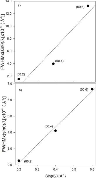
The mosaic crystallite size and
tiltcalculated from the Hexagonal (0002), (0004) ve (0006) miller plane of rocking curve using Williamson–Hall equation [22, 23] in Fig 3. The mean
tilt is obtained from the slope of the linear dependence andL
P
0.9 /(2
y
0)
from the inverse of the y-intersection yo of the fitted line with the ordinate from the plot of the FWHM(sin ) /
function against
(sin ) /
function (W-H plot). In the function expression, FWHM is in half width of rocking curve scans,
is the Bragg reflection angle, and
is wavelength of CuK1. The expected linear behavior ofİlknur KARS DURUKAN, Mustafa Kemal ÖZTÜRK, Süleyman ÖZÇELİK, Ekmel ÖZBAY / Journal of Polytechnic, 2017; 20 (3) : 531-536
the graphs is experimentally well confirmed, which gives the rather accurate tilt angle values. The mean
tilt values of the samples are 0.11x10⁻² and 0.3x10⁻² degree, respectively. It can be seen in this table that the mean tilt angle for the second sample is the higher than first sample sample. TheL
P of the HR-GaN epilayers were determined and this values are 6.43x10⁴ nm and 9x10² nm, respectively. The maximumL
P values were observed for first sample.Figure 3. Williamson–Hall curves for GaN of a) first sample and b) second sample for tilt and lateral coherence length calculation
Twist angle calculated from FWHM values of the reflection peaks of the "Rocking" and "Phi" scans of the hexagonal (12-31) planes. Twist angle values of LED samples are 0.117 and 0.858, respectively. The screw and edge type dislocations of LED samples were calculated. Dislocations were calculated by the equations below [24].
𝑁𝑠𝑐𝑟𝑒𝑤= 𝑎𝑤2
4.35|𝑏|2 (2) Screw type discontinuity equation (Eq.2), w stands for tilt angle and b, Burgers vector (0.519 nm for screw dislocation). The Burgers vector equals the lattice parameters. Screw type dislocation values of LED samples are 0.32x10⁵ and 2.34x10⁵, respectively. Edge type dislocation equation (Eq.3), b is Burgers vector length (Burger vectors are 0.39 nm for edge dislocation). Here, a is the half-width peak of the asymmetric plane is related with twist and LII, stands for lateral mosaic coherence length. Edge type dislocation values of LED samples are 0.568x10⁷ and 2.74x10⁹, respectively.
𝑁𝐸𝑑𝑔𝑒 = 𝑎∅
2.1|𝑏|𝐿𝐼𝐼 (3)
The optical characteristics of the InGaN LED structures were investigated by PL measurement. Figure 4 shows the room temperature PL spectra of the two samples. The experimental results are shown with solid lines and their Gaussian fits are shown with dashed lines. Usually, The PL spectrum from InGaN LEDs shows two emission peaks, which are at the blue and yellow regions. In our work, It can be seen that the two peaks blue-green and a green PL emissions of first sample are centered around 493 nm, 520 nm and 550 nm, respectively. First sample has a wider well width than second sample. Therefore, This situation will result in a significant blueshift when plenty of carriers are injected to produce the screening effect. In second sample, two kind of emission were observed in green and yellow emissions, centered around 543 nm and 587 nm, respectively. In second sample, the rate of indium is higher than first sample. When the In ratio is higher, emission shifts to red. For white LED applications, this is an undesirable situation. First sample is suitable for White LED applications.
Figure 4. PL intensity versus wavelenght of the two samples.
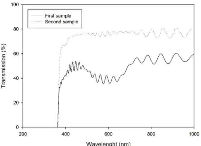
The transmission of the InGaN LED structures were investigated by UV analysis. Figure 5 shows the transmission spectra of first sample and B. As can be seen
in the graphic, the first sample has a trasmission of about 80 and the second sample has a transmission of about 60 percent. As the In ratio increased, the ratio of In in the second sample is less,the trasmittance decreased. Also, In the second example, although the well width is narrow, the trasmittance is reduced due to the interface roughness. Due to the 5-layer InGaN / GaN multi-quantum well in the structure, large amplitude oscillation occurs. Also, The between the 5-layer multi-quantum well and GaN layer has a low amplitude and frequent frequency interference, There is no distinction between these two interference.
Figure 5. Variation of transmittance with the wavelength for two samples
4. CONCLUSION
The crystals formed in the structure of the first sample are larger. When these crystals are formed, the lattices are reformed due to the effects of biaxial strain in the c and a direction and hydrostatic strain and high stresses. These stresses are commonly known. This occurs when the structure is being cooled from the growth temperature to lower temperatures. These stresses increase the FWHM of the crystal plane peak, making it distorted This does not affect the reduction of the value of the edge dislocation, twist and plane tilt angle of the structure. In Example B, while the FWHM is lower, the crystal size is reduced even though the stress is reduced. And as the crystal size decreases, the edge dislocation, twist, plane inclination angle, which is characteristic of the defect, increases. These biaxial a and c hydrostatic pressure values tend to decrease as point defects can not settle in the structure. As a result, the quality of LEDs can be easily observed with detailed high resolution x-rays. In this case, we can say that the crystal size of first sample is larger than second sample. Although Second sample has low FWHM values, Interface roughness, low number of fringe peaks, and low intensity values of these peaks are the proof the of defect. Even if AlN is lower than the half-width of the buffer layer, it does not change. This may be due to a problem caused by the nucleation layer. The PL spectrum from InGaN LEDs showed that In ratio is higher, emission shifts to red. In addition, The
transmission of the InGaN LED showed that the ratio of In increases, trasmittance decreases.
REFERENCES
1) Chen H.-S., Yeh D.-M., Lu C.-F., Huang C.-F., Lu Y.-C., Chen C.-Y., Huang J.-J., and Yanga C. C., “Mesa-size-dependent color contrast in flip-chip blue/green two-color InGaN/GaN multi-quantum-well micro-light-emitting diodes”, Applied Physics Letters, 89: 093501, (2006). 2) Öztürk M.K., Çörekçi S., Tamer M., Çetin S.S., Özçelik
S. And Özbay E. “Microstructural properties of InGaN/GaN light-emitting diodestructures with different In content grown by MOCVD”, Applied Physics A, 114: 1215–1221, (2014).
3) Yeh D.-M., Huang F., Chen H.-S., Tang T.-Y., Lu C.-F., Lu Y.-C., Huang J.-J., Yang C. C., Liu I-S. and Su W.-F., “Control of the color contrast of a polychromatic light-emitting device with CdSe–ZnS nano-crystals on an InGaN–GaN quantum-well structure”, IEEE Photonics
Technology Letters, 18: 5, (2006).
4) Chen H.-S., Yeh D.-M., Lu C.-F., Huang C.-F., Shiao W.-Y., Huang J.-J., Yang C. C. Liu I.-S. and Su W.-F. “White light generation with CdSe–ZnS nanocrystals coated on an InGaN–GaN quantum-well blue/green two-wavelength light-emitting diode”, IEEE Photonics
Technology Letters, 18:13, (2006).
5) Yamada M., Narukawa Y. and Mukai T., “Phosphor free high-luminous-efficiency white light-emitting diodes composed of InGaN multi-quantum well”, Journal
Applied Physics, 41: L246–L248, (2002).
6) Damilano B., Grandjean N., Pernot C. and Massies J. “Monolithic white light-emitting diodes based on InGaN/GaN multiple quantum wells”, Journal Applied
Physics, 40: L918–L920, (2001).
7) Shei S.C., Sheu J.K., Tsai C.M., Lai W.C., Lee M. L. and Kuo C.H., “Emission mechanism of mixed-color InGaN/GaN multi-quantum-well light-emitting diodes”,
Japanese Journal of Applied Physics, 45: 2463–2466,
(2006).
8) Huang C.F., Lu C. F., Tang T. Y., Huang J. J. and Yang C. C., “Phosphor-free white-light light-emitting diode of weakly carrier-density-dependent spectrum with prestrained growth of InGaN/GaN quantum wells”,
Applied Physics Letters, 90: 151122, (2007).
9) Yamada M., Narukawa Y., Tamaki H., Murazaki Y. and Mukai T.,"A methodological study of the best solution for generating white light using nitride-based light-emitting diodes", IEICE Trans. Electron. IEICE TRANSACTIONS on Electronics, E88-C: 1860, (2005).
10) Leszczynski M., Teisseyre H., Suski T., Grzegory I., Bockowski M., Jun J., Pakula K., Baranowski J.M., Foxon C.T. and Cheng T.S., “Lattice parameters of gallium nitride”, Applied Physics Letters, 69:73, (1996). 11) Cho S. I., Chang K. and Kwon M. S., “Strain analysis of a GaN epilayer grown on a c-plane sapphire substrate with different growth times”, Journal of Materials
Science, 42: 3569–3572, (2007).
12) Harutyunyan V.S., Aivazyan A.P., Weber E.R., Kim Y., Park Y., Subramanya S.G., “High-resolution x-ray diffraction strain-stress analysis of GaN/sapphire heterostructures”, Journal of Physics D: Applied
İlknur KARS DURUKAN, Mustafa Kemal ÖZTÜRK, Süleyman ÖZÇELİK, Ekmel ÖZBAY / Journal of Polytechnic, 2017; 20 (3) : 531-536
13) Kittel C., “Introduction to solid state physics”, John
Wiley & Sons, Singapore, 8, (1991).
14) Gil, B., “Group nitride semiconductor compounds”,
Oxford University Press Inc., Oxford, 1, (1998).
15) Edgar J.H., Strite S., Akasaki I., Amano H. And Wetzel C., “Properties, processing and applications of gallium nitride and related semiconductors”, INSPEC, London, 381, (1999).
16) Kisielowski C., Kruger J., Ruvimov S., Suski T., Ager J. W., Jones E., Liliental-Weber Z., Rubin M., Weber E. R., Bremser M.D. and Davis R. F., “Strain-related phenomena in GaN thin films”, Physical review B, 54: 17745, (1996).
17) Kisielowski C., “Strain in GaN thin films and heterostructures”, Semiconductors and Semimetals, 57: 275-317, (1999).
18) Perry W. G., Zheleva T., Bremser M. D., Davis R. F., Shan W. and Song J. J. ,“Correlation of biaxial strains, bound exciton energies, and defect microstructures in gan films grownon AIN/6H-SiC(0001) substrates”, Journal
of Electronic Materials, 26: 224, (1997).
19) Skromme B. J., Zhao H., Wang D., Kong H. S., Leonard M. T., Bulman G. E. and Molnar R. J.,”Strain determination in heteroepitaxial GaN”, Applied Physics
Letters, 71: 829, (1997).
20) Cetin S. S., Öztürk M. K., Özcelik S., Özbay E., “Strain analysis of InGaN/GaN multi quantum well LED structures”, Crystal Research and Technology, 47: 824– 833, (2012).
21) Polian A., Grimsditch M. and Grzegory I., “Elastic constants of gallium nitride”, Journal of Applied
Physics, 79: 3343, (1996).
22) Metzger T., Höppler R., Born E., Ambacher O., Stutzmann M., Stömmer R., Schuster M., Göbel H., Christiansen S., Albrecht M. and Strunk H.P., “Defect structure of epitaxial GaN films determined by transmission electron microscopy and triple-axis X-ray diffractometry”, Philosophical Magazine a-Physics of
Condensed Matter Structure Defects, 77: 1013, (1998).
23) Williamson G. K. and Hall W. H., “X-ray line broadening from filed aluminium and wolfram”, Acta
Metallurgica, 1: 22, (1953).
24) Kars Durukan İ., Öztürk M. K., Çörekçi S., Tamer M., Bas Y., Özçelik S. and Özbay E., “Microstructural analysis with graded and non-graded ındium in ıngan solar cell”, Journal of Nanoelectronics and Optoelectronics, 12: 109–117, (2017).