Chemically Specific Dynamic
Characterization of Photovoltaic and
Photoconductivity Effects of Surface
Nanostructures
Okan O¨ ner Ekiz,* Koray Mizrak, and Aykutlu Daˆna*
UNAM Institute of Materials Science and Nanotechnology, Bilkent University, 06800 Ankara, Turkey
X
-ray photoelectron spectroscopy (XPS) is a powerful spectroscopic technique for the characterization of surfaces with chemical specificity.1⫺5The photoelectron spectra carries information about the binding states of different atomic species within tens of nanometers of the surface, as well as information on local po-tential variations. If the emitted electrons are not compensated by an external elec-tron gun or directly from the substrate, lo-cal potentials can vary due to lolo-cal conduc-tivity variations that result in different amounts of accumulated charge. Over-charging by injection of excess electrons was previously used for surface character-ization.6Surface potentials can be shifted by direct application of a voltage to the sub-strate. Such shifts resulting from direct volt-age stimulus were previously modeled for static and dynamic voltage excitations, tak-ing into account conductivity and capaci-tances of surface domains.7⫺13 Nano-structures are increasingly findingapplication in photovoltaic technologies. In-vestigation of photovoltaic and photocon-ductivity effects in nanowires, nanocrystals, and nanocomposites are interesting from a fundamental scientific point of view. Con-ventional characterization techniques lack chemical specificity, and most of the time require precision fabrication of contacts on nanostructures using techniques such as electron beam lithography or related lithog-raphies with nanoscale resolution, espe-cially if single nanoparticles are involved. Surface photovoltage spectroscopy (SPV) has been traditionally applied to character-ize photoinduced surface photovoltage changes upon illumination, using the Kelvin probe as a readout method for surface
po-tential shifts.14,15Also, Kelvin probe micros-copy has been used to observe photovol-taic effects on nanoscale structures.16The chemically specific readout of photoin-duced surface potential changes is a highly desirable analytical capability. Such chemi-cally specific measurements are not pos-sible with conventional Kelvin probe mea-surements. Previously, XPS has been used to probe the surface photovoltage of silicon surfaces.17Recently, Cohen18,19et al. demon-strated that surface potential shifts related to external illumination were observable in XPS spectra of composite semiconductor surfaces. It was demonstrated that static or quasi-static shifts of XPS peaks can be re-lated to photovoltaic and photoconductive effects. The shifts can be quantitatively studied with films on conductive substrates.18,19
In this article we demonstrate an ap-proach that allows the study of photovol-taic and photoconductivity effects using the XPS, under static or modulated illumina-tion. Surface potentials of domains are in-ternally modulated owing to both photo-voltaic and photoconductivity effects. We show that a circuit model can be used to
*Address correspondence to [email protected], [email protected]. Received for review October 15, 2009 and accepted March 30, 2010.
Published online April 9, 2010.
10.1021/nn9014196
© 2010 American Chemical Society
ABSTRACT We report characterization of photovoltaic and photoconductivity effects on nanostructured surfaces through light induced changes in the X-ray photoelectron spectra (XPS). The technique combines the chemical specificity of XPS and the power of surface photovoltage spectroscopy (SPV), with the addition of the ability to characterize photoconductivity under both static and dynamic optical excitation. A theoretical model that quantitatively describes the features of the observed spectra is presented. We demonstrate the applicability of the model on a multitude of sample systems, including homo- and heterojunction solar cells, CdS nanoparticles on metallic or semiconducting substrates, and carbon nanotube films on silicon substrates.
KEYWORDS:X-ray photoelectron spectroscopy · carbon nanotubes · cadmium sulfide · silicon · dynamic characterization · surface photovoltage ·
photoconductivity · semiconductor nanoparticles · photovoltaics
estimate the changes in spectra under static and dy-namic illumination conditions. Light-induced surface potential differences due to photovoltaic and photo-conductive effects can be identified.
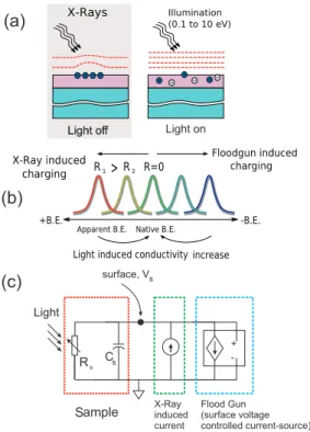
The general behavior of change in surface poten-tials due to photovoltaic and photoconductive effects are schematically summarized in Figure 1 and Figure 2. When light is absorbed by nanoscale semiconducting domains, generated carriers diffuse and drift due to in-ternal electric fields. Carriers may accumulate in differ-ent regions of nanostructures or escape to the sub-strate. Variations in surface state densities, material composition, or doping may be responsible for the cre-ation of nanoscale junctions displaying photovoltaic ef-fects. Photoinduced potential differences between the ground plane and surface domains can arise, as sche-matically shown in Figure 1a. If the domain has a p-type top surface (vacuum interface), the binding energies on the surface tend to shift toward positive energies. If the domain has an n-type top surface, the shift is to-ward negative binding energies. X-ray or external electron-injection related charging results in local varia-tions of surface potentials.6If the surface has finite con-ductivity, X-rays cause a positive charge build-up and the surface potential shifts toward positive energies (Figure 2b). In the presence of an electron flood-gun, the surface charge is compensated by externally
in-jected electrons. If more electrons are inin-jected than lost by photoelectron emission, the surface may be negatively charged and the spectra displays a shift to-ward negative binding energies. If the conductivity of the surface layer is increased by application of an exter-nal light source (photoconductive effect), the charge build-up is decreased due to compensation by avail-able carriers. Photoconductivity causes the peaks to re-turn closer to the native binding energy for both posi-tively and negaposi-tively charged surfaces (Figure 2b).
In an arbitrarily complex composite film, different re-gions of the film may display both photoconductive and photovoltaic effects. The mechanisms shown in Figure 1 and Figure 2 may be acting in series or paral-lel combinations. Simple lumped circuit models as shown in Figure 1c and Figure 2c can be used to study the dynamic behavior due to photovoltaic and photo-conductive effects. Simplified models include a single photovoltaic junction or a light-controlled resistance. The circuits are driven by the photocurrents generated in the junction as well as by external currents due to X-ray illumination and electron injection by the flood-gun. The models for photovoltaic and photoconductive cases can be combined in series or parallel cascades, if both effects are simultaneously present. A feature com-mon to all cases is the external current source. The ex-Figure 1. (a) Surface potential distribution of a composite
surface containing n and/or p-type domains can be per-turbed upon illumination by light (0.1ⴚ10 eV photons) due to the photovoltaic effect. (b) Resulting potential shifts can be observed in the XPS spectra. A pⴚn junction is character-ized by a shift of the surface potential to positive binding en-ergies and an nⴚp junction causes a negative shift. (c) A sim-plified lumped circuit model including a single junction can be used to describe static and dynamic behavior of the sur-face photovoltaic effect.
Figure 2. (a) Surface potentials can shift due to X-ray or flood-gun induced charging. (b) Excess positive charge due to X-ray illumination causes a positive shift, and excess nega-tive charge due to electron injection by the flood-gun causes a negative shift. The shifts are proportional to the resis-tance between the surface and ground. Upon illumination, resistance is reduced and peaks return to the uncharged (na-tive) binding energy. (c) A simplified lumped circuit model can be used to describe the time dependent surface poten-tial due to static or dynamic photoconductivity.
ternal surface current Iscan be expressed as the sum of the escaping photoelectron current Ix(a constant, proportional to the X-ray photon flux intensity) and the flood-gun current IFG(Vs, VFG). The flood-gun current can be approximated by IFG(Vs, VFG)⬵ ⫺IFG0[1⫹ tanh (␣(Vs⫺ VG0⫹ VG))]/2, where Vsis the surface voltage, VFGis the flood-gun bias, VG0is a constant offset, IFG0is the maximum electron current achievable from the flood gun and␣ is an experimental parameter. This general form of the IFG(Vs, VFG) is chosen so that the ba-sic phyba-sical mechanism of electron charging of surfaces are included in the model with few adjustable param-eters. Electron injection by the flood-gun is dependent on the surface potential, and there are few different characteristic regimes. If the surface potential becomes negative, the flood-gun electrons are repelled from the surface causing a decrease of current. If the surface po-tential becomes positive, electron capture rate in-creases. There is a range of positive surface potentials where the electron current is linearly proportional to the surface potential. Owing to the finite availability of electrons, above a certain positive surface voltage, elec-tron current does not further increase and reaches a saturation value IFG0.
RESULTS AND DISCUSSION
We investigate the validity of the model by consid-ering samples which demonstrate dominantly photo-voltaic or photoconductive effects, as well as the simul-taneous presence of both. It is known that light-induced carrier generation and diffusion may disturb the sur-face pinning and can cause band bending in semicon-ductors. Therefore, bare semiconductor surfaces may show some degree of surface photovoltaic (SPV) effect. The magnitude and sign of the surface photovoltaic ef-fect depend on many parameters, such as the distribu-tion of surface density of states, the bulk Fermi level po-sition, and mobilities. Such SPV effects can be observed using the XPS, as is demonstrated in Figure 3. Since sili-con substrates are used in the experiments involving nanoparticles, we first characterize the SPV of the sub-strates. When an n-type silicon surface (nominal resistiv-ity 1⫺10 Ohm-cm) is illuminated with white light, there is no identifiable shift (Figure 3a). However, when a p-type silicon surface (resistivity 1⫺10 Ohm-cm) is illu-minated with white light, a surface potential shift of ⫺0.13 eV is observed (Figure 3b). Such shifts have been previously characterized as a function of doping den-sity and type. It is known that p-type silicon produces a greater shift for a given doping level.14A greater dop-ing level is known to reduce the SPV. Our observation is in agreement with the previous studies, if it is as-sumed that the actual doping level of the n-type sub-strate is higher than p-type. To unambiguously demon-strate photovoltaic effects, ideal p⫺n and n⫺p junctions are studied. Two silicon solar cells were stud-ied. The photovoltaic effect can be observed as shown
in Figure 3c and Figure 3d on both n⫺p and p⫺n junc-tions. The Si 2p peak in the XPS spectra of an n⫺p junc-tion (top side n, bulk of the substrate p-type) from a commercial monocrystalline solar cell is shown to shift toward negative binding energies (Figure 3c). The shift direction is reversed for the p⫺n junction (top side p-type, bulk of the substrate n-type). The magnitude of the shift can be estimated using the model in Fig-ure 1c. The shunting resistance RSHin the model may be an internal resistance, or may be due to grounding of the top surface by an external resistance. In our XPS system, the samples are mounted using insulating clamps or bronze clamps, which act as resistive ground-ing paths. The effect of the extra ground path is ob-served in the surface potential for an n⫺p silicon junc-tion (Figure 3e and Figure 3f). As the spectra is collected close to a grounded metal contact, surface potential shifts are decreased. As we move further away from the grounded contact, the surface potential shift increases to negative values (Figure 3f). The deviation of the sur-face potential from linear can be understood using a distributed circuit model. We can divide the photovol-taic cell into smaller cells connected to each other by small series resistances. Because of the nonlinear IV characteristics of individual cells, we observe an abrupt shift of the surface potential. The location of the abrupt Figure 3. Surface potential of a bare silicon surface is not signifi-cantly affected by illumination for an (a) n-type substrate, but (b) a shift ofⴚ0.13 eV is observed for a p-type substrate. When fabri-cated (c) nⴚp and (d) pⴚn junctions are illuminated; apparent binding energy shifts by VOCare observed. Note that the signs of
the shifts are as expected, negative for the nⴚp junction and posi-tive for the pⴚn junction. (e) Light induced surface potentials can also be mapped spatially by measuring at different locations on the sample.
change depends on the ratio of cell currents and cir-cuit resistances. The XPS data is a result of the convolu-tion of the spot-size of the spectrometer and spatial variations of the surface potential. This causes smooth-ing of the voltage profile.
To demonstrate photoconductive effects, CdS nano-particles were studied on a variety of substrates. XPS spectra of CdS particle film on a grounded Au/Pd sur-face were recorded under dark and illuminated condi-tions as shown in Figure 4a. Here the flood-gun is turned off, and all charging is due to X-ray induced charging. In the spectra, two distinct peaks are identifi-able in the Cd 2d spectrum. In the dark, X-ray charging is seen to cause a shift of one of the peaks toward posi-tive binding energies (408.15 eV for Cd). As the sample is flooded with white light from a superbright LED, this peak shifts toward the native binding energy of Cd in CdS. The smaller peak in the spectrum, originally at 405.4 eV shifts only 0.1 eV to 405.33, which is very close to the original position of cadmium peak for CdS.20We attribute this peak to the particles that are directly in contact with the surface (regions with monolayer or submonolayer coverage).
The charging effect due to the flood-gun electrons is also shown in Figure 4b. XPS spectra of a CdS nano-particle film on a n-doped silicon substrate is recorded under dark and illuminated conditions. The flood-gun voltage VGwas set to 0 and 4 V. The convention for the sign of the flood-gun voltage is equipment depend-ent. In our case a positive VGcauses increased electron charging. Under dark conditions and VG⫽ 0 V, a positive shift is observed. The positive shift is a result of X-ray re-lated charging. For VG⫽ 4 V, electron charging
be-comes dominant, and a negative shift of the Cd peak
is observed. As the sample is illuminated, both positive and negative shifts decrease. The peaks return closer to the native binding energy. This is attributed to the in-crease in the conductivity of the CdS film.
A more general case is the simultaneous pres-ence of both photoconductivity and photovoltaic ef-fects. Band alignment and photovoltaic effects of CdS/p-Si heterojunctions has been previously studied.21,22In general photoconductive effect re-sults in a decrease of the charging related shifts and photovoltaic effects cause an increase in the magni-tude of shifts. However, with multiple unknowns about a specific sample, it is not possible to sepa-rate the two effects without the addition of a swept parameter. The flood-gun potential can be used for this purpose. The surface potential shifts as the flood-gun bias is changed from 0 to 4 V, inducing controlled hole or electron charging. Illumination re-duces the resistance, and magnitudes of positive and negative shifts are both reduced. When the peak positions are plotted versus flood-gun potential, if the photovoltaic effect is not present, the curves for dark and illuminated conditions show a crossing-over behavior. This is because there exists a flood-gun potential VG,0for which the X-ray induced current is canceled by electron injection. At this flood-gun voltage, charging is zero regardless of the sample resistance Rs, causing the dark/light curves to cross. If a photovoltaic effect is present, the curves may not cross owing to the shift caused by the photovoltage. The crossing-over or noncross-ing over behavior depends on the relative strengths of the photovoltaic and photoconductive effects. The sign of the photovoltage is also a factor in the determination of the crossing/anticrossing behavior. We demonstrate these effects using samples that show both photoconductivity and photovoltaic ef-fects are present. We measure the XPS spectra of films of CdS nanoparticles on n- and p-type silicon as a function of VG(Figure 5). CdS forms an n⫺p junction on p-type silicon and displays both photo-voltaic and photoconductive effects. CdS films on an n-type silicon substrate show photoconductivity dominantly. For n-type silicon, a crossing of the peak energies is observed under dark and illuminated conditions. The experimental data in Figure 5a can be qualitatively reproduced assuming the presence of a photoconductive effect Figure 5b. This observa-tion suggests the absence of a strong photovoltaic effect between the n-type CdS film and n-type Si. For CdS on p-type silicon, the photoconductivity of the nanoparticle film is accompanied by the photovol-taic effect between the CdS/p-type silicon.
The wavelength dependence of the effects can be seen in Figure 5c. The CdS film on a p-type silicon sub-strate is illuminated with 532 (2 mW nominal power) and 650 nm (1 mW nominal power) lasers. CdS nano-Figure 4. (a) Photoresponse of CdS nanoparticles on a
grounded AuPd surface; (b) photoresponse of CdS nanoparti-cles on n-type silicon (experimental data, left), where X-ray charging is dominant (VFGⴝ 0) and electron charging is
domi-nant (VFGⴝ 4V) in the dark. In both cases, illumination causes
reduction of charging. The peaks tend to shift toward the na-tive binding energy (schematic description, right).
particles have a bandgap above 2.42 eV,23therefore no absorption is expected for 650 nm illumination in the CdS layer. Here, the flood-gun is turned off and all charging is due to X-ray exposure. The CdS layer re-mains charged under 650 nm illumination. However, p-type silicon shows a shift of⫺0.13 eV (as was previ-ously observed on a bare p-type sample, shown in Fig-ure 3b). Since the CdS film is referenced to the silicon
surface, the apparent binding energy of Cd3d is also shifted by⫺0.13 eV. When the sample is illuminated us-ing 532 nm laser, both CdS and Si display photoactiv-ity, Cd3d shifting as much as⫺2.5 eV. The photocon-ductivity related shift of the Cd3d line on an n-type substrate is about⫺2.1 eV, with no significant shift of the Si peak. We therefore conclude that the CdS/p-Si junction displays a photovoltage of about⫺0.27 eV. For Figure 5. (a) Light-induced changes in the XPS spectra of Cd from CdS nanoparticles on n- and p-type silicon sub-strates as a function of the flood-gun potential. Peak positions are plotted for dark and illuminated cases showing sig-nificantly different behavior. (b) Theoretical model can be used to predict a similar behavior for the n-type CdS on n- and p-type silicon. The change from crossing to noncrossing curves are attributed to the presence of a photovol-taic effect for the n-CdS/p-Si case. The anticrossing behavior is not universal but is dependent on experimental and sample related parameters such as the total induced photovoltage at the junction, floodgun and X-ray induced sur-face currents, and strength of the photoconductivity effect. (c) Photoconductive and photovoltaic effects are also shown to be wavelength dependent: When illuminated by 532 nm light (above the CdS bandgap), both CdS and sili-con display light-induced effects, silisili-con showing only surface photovoltaic effect and CdS displaying both photovol-taic and photoconductive effects. When illuminated by a 650 nm laser, the sample absorbs light only in the p-type sili-con substrate producing shifts equal to the silisili-con surface photovoltage shown in Figure 3b. In this case, the apparent CdS binding energy follows the potential of the silicon substrate it rests upon.
CdS/p-type silicon, there are two photovoltaic junc-tions (CdS/p-Si and p-Si surface) and a single photocon-ductive region (CdS), all acting in series. Wavelength de-pendent measurement allows us to distinguish shifts due to individual junctions.
Previously dynamic characterization of surface volt-age distributions were carried out using externally
modulated sample bias. A simplified RC model of a composite surface was shown to quantitatively predict XPS spectra. The convolution approach used for simula-tion of XPS spectra under dynamic excitasimula-tion24can be extended to include the photoeffects using the model shown in 1c. A p⫺n junction (ALIC cell) is placed inside the XPS chamber and subjected to static and modu-lated illumination by an external laser (650 nm, multi-mode diode laser, 0.5 mW) with modulation frequen-cies ranging from 0.1 Hz to 1 MHz, while the
photoelectron spectra are collected. The surface poten-tials of various domains on the device are modulated according to their local electronic properties. The elec-tronic properties determine the equivalent lumped cir-cuit elements such as capacitances, shunt, and series resistances.
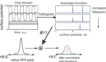
We demonstrate the applicability of the technique on a p⫺n junction known to display the photovoltaic effect dominantly. We use the model in Figure 1 in a cir-cuit simulator to calculate the dynamic response of the lumped circuit. The time-dependent surface poten-tials are calculated with the simulator, then the line shape functions g() are calculated using a histogram of the time-series of the surface voltage. The lineshapes are then used to estimate the peak position shifts and broadenings as described elsewhere.25It is seen that, if the frequency of modulation is slow compared to the characteristic cutoff frequency of the surface response, the line shape function resembles a double delta func-tion separated by VOC(Figure 6). The resulting con-volved peak shape has a greater width and reduced peak intensity. The peak position is shifted to about VOC/2. As the modulation frequency is increased above the cutoff frequency of the junction, the junction acts like a low-pass filter. In this case, the line shape be-comes like a single delta function. The width of the ob-served peak becomes narrower, closer to the native width of the peak. This is accompanied by a slight shift of the peak position toward VOC. Simulation results for
Figure 6. Surface voltages under modulated illumination are calculated using the simplified circuit model. Time varying surface potentials are used to calculate line shape function g() using a histogram. The line shape function is then convo-luted with the original unmodulated XPS data to predict spectra under modulated illumination.
Figure 7. (a) Apparent binding energy and full-width-at-half-maximum of the oxygen peak on a pⴚn ALIC cell as a function of modulation frequency is shown. Theoretical model assumes VOCⴝ 0.53 V and RSHⴝ 850 ⍀ extracted from the IⴚV
measure-ments on the same cell. The capacitance value (Cⴝ 200 nF) is obtained by fitting. (b) The frequency dependence of apparent binding energies of residual aluminum, collected at points close to and away from the contact, is shown. Slightly different fre-quency responses are observed.
the ALIC cell, using parameters extracted from dark and illuminated I⫺V curves are shown in Figure 7. The model predicts the correct form of frequency depen-dence. It is seen that when model parameters obtained by conventional device characterization methods are used, theoretical calculation of the peak shifts and broadening agree with the XPS measurements. This ob-servation suggests that model parameters of solar cells can be extracted through numerical analysis and using XPS measurements only. In principle, correlations of op-toelectronic properties can be established between dif-ferent peaks automatically. Similar correlations of elec-tronic properties were extracted using modulated external bias.24,26Location dependent dynamic charac-terization is also possible. Changes in the SPV frequency response can be observed if the response is measured close to or away from the contacts (Figure 7b)
The photoconductivity can be studied dynamically as well as through photovoltaic effects. We use pulsed illumination on a CdS nanoparticle film on an n-type substrate. Light pulses of durationpulse⫽ 5 ms with a repetition rate frepis incident on the sample. A super-bright white LED is used as the light source. The flood gun is turned off and only X-ray gun charging is present. During the light pulse, photoconductivity reduces the resistance of the film (R⫽ Ron⬇ 0). In this period, the surface may be thought as shorted to ground. During the dark period, the surface behaves like an an RC cir-cuit (R⫽ Roff⬇ 30 M⍀, C ⬇ 0.2 nF), charged by the X-ray current (Ix⯝ 100 nA). The circuit element values are ob-tained by fitting. If the pulse repetition rate is increased, the film spends more time in the short state. Therefore, at low frequencies the film is mostly charged and at high frequencies the film is mostly shorted. The gradual transition between fully off and fully on states can be observed in the XPS data (Figure 8a). When the pulse frequency is close to the effective RC time constant of the film, maximal peak broadening occurs. This feature, theoretically estimated by the model, can be observed in the experimental results shown in Figure 8b.
We apply the technique to the characterization of light induced changes in the XPS spectra of single and multiwalled carbon nanotubes (SWCNT and MWCNT) on metal and semiconductor substrates. Electronic structure and properties of SWCNTs and MWCNTs have been extensively studied both theoretically and experimentally.27⫺33Also CNTs have found application in photovoltaic devices both as contacts and active layers.34⫺40For the sake of simplicity, the experiments were performed without activating the flood-gun. In this case, all charging must be due to X-ray related charging. It is observed that the carbon peak from a thin film of MWCNTs on a n-type silicon surface demon-strates a shift of⫹0.3 eV upon illumination (Figure 9b). No significant shifts are observed on p-type silicon or on AuPd-coated substrates. A similar shift is observed with a SWCNT film on n-type silicon substrates. When
the native oxide layer (typically few nm thick) on the substrate is cleaned using HF prior to casting of the CNT film, it is observed that the light induced shift is de-creased (Figure 9e). Since only X-ray charging is pos-sible without the flood-gun, in this case the photocon-ductive effect may only produce a negative shift, in favor of reducing charging. As the observed light-induced shift is positive, it is due to the photovoltaic ef-fect, the CNT film acting effectively as a p-type domain on an n-type substrate. This conclusion is also sup-ported by observation of the effect only on n-type sub-strates. To understand the origin of the observed shift, we model the electrostatic problem at the CNT/oxide/ silicon interface under illumination using rate equa-tions, taking into account the
generation⫺recombination and electron/hole tunnel-ing rates as shown in Figure 9a. We assume carrier gen-eration in the CNT film only. In CNTs, the electron and hole properties are highly symmetric,28,41and we may assume a density of states for the CNT ensemble sym-metric around the CNT affinity of 4.5 eV.35,42,43We as-sume that the relaxation inside the CNT film is rapid, and the CNT film is in equilibrium, with separate quasi Fermi levels for electrons and holes. We also assume that the escape rates of carriers to the substrate are Figure 8. The effect of pulsed illumination on the Cd3d peak for a CdS nanoparticle film on n-type silicon. Because of modulation of CdS film conductivity by a 5 ms long light pulse of varying repetition frequency, the charging is inter-mittently reduced. The flood-gun is turned off and X-ray re-lated positive charging is present only. (a) The peak position shifts as a function of repetition frequency frep. (b)
Broaden-ing of the peak is observed when pulse-to-pulse separation time is near the effective RC time constant of the film. Experi-mental observations can be understood using the model given in Figure 2. R and C values, as well as the X-ray in-duced current Ixare fitting parameters. Satellite graphs show
theoretically calculated transient surface potentials for slow and fast pulse repetition rates.
dominated by direct tunneling rates. Under these sim-plifying assumptions, the net charge on the CNT film and resulting surface potential is determined by an im-balance between the electron and hole tunneling rates rnand rp.44,45Under illumination, carrier generation and recombination rates, G and R are related to escape rates and carrier concentration change rates by⌬n/t ⫽ G ⫺ R ⫺ ⌬nrn(Fox) and⌬p/t ⫽ G ⫺ R ⫺ ⌬prp(Fox) where Foxis the barrier (oxide) field. At a given time, the elec-tron and hole concentrations in the CNT film are⌬n and ⌬p, giving a net charge concentration of ⌬q ⫽ ⌬p ⫺ ⌬n. The barrier field is related to charge on the CNT film by Fox⯝ ⌬q/2ox. Under steady state conditions,⌬n/t ⫽ ⌬p/t ⫽ 0 and ⌬nrn(Fox)⫽ ⌬prp(Fox). The surface po-tential shift⌬Vs⯝ Foxtox, where toxis the oxide (barrier) thickness. The net charge can be rewritten as⌬q ⫽ ⌬p ⫺ ⌬n ⫽ ⌬n(rn(Fox)/rp(Fox)⫺ 1). The tunneling rates rnand rpare assumed to be determined by direct tunneling. For small barrier fields (Fox⬇ 0), ri⬀ exp(⫺3Bi公VB,Itox/ 2), where Bi⫽ 4(2mox,iq)1/2/3ប; VB, iis the barrier height
for tunneling and mox,iis the tunneling effective mass.46⫺48Hence, tunnel rates are exponentially de-pendent on the electron and hole barriers (VB,e⯝ 4.5
and VB,p⯝ 4.66 eV) and barrier thickness tox, electron tunneling being typically faster. Hence, a positive net charge accumulates on the CNT film and a surface po-tential shift⌬Vsproportional to the oxide thickness is
expected. As the surface potential shift increases, changing barrier field tends to readjust the electron and hole escape rates and an equilibrium value propor-tional to the oxide thickness is achieved. The estima-tions of this model agree with the observaestima-tions shown in Figure 9d and Figure 9e, where a decrease of the sur-face photovoltage is seen for reduced barrier thick-ness. The observed photovoltage polarity is in parallel with previous demonstrations of solar-cells made up of carbon-nanotube films on n-type silicon.39
CONCLUSION
We present an extended model of surface poten-tials in an XPS experiment in the presence of photovol-taic and photoconductive effects. The approach is shown to distinguish between surface voltage shifts due to photovoltaic or photoconductive effects. The model also can be used to predict dynamical behavior of surface voltages under modulated illumination. Wavelength dependent absorption and chemically spe-cific response is observed in composite surfaces. The origins of the shifts can be understood by referring to the predictions of the presented model. The method can be used in combination with standard XPS proce-dures, such as depth profiling and angle resolved XPS, to provide greater insight into the origins of optoelec-tronic effects. The demonstrations also underline the importance of illumination in an XPS experiment.
EXPERIMENTAL SECTION
The surface photovoltaic effects were observed on shallow p⫺n and n⫺p junctions. The n⫺p junction was a commercial sili-con photodiode produced by POCl3based diffusion. The p⫺n
junction was made in-house by metal induced crystallization. The device studied in the experiments were fabricated by depos-iting a nominally 400 nm thick amorphous silicon (a-Si) layer onto a hydrofluoric acid (HF) cleaned n-type silicon wafer (1⫺10 Ohm cm nominal resistance) using plasma enhanced chemical
vapor deposition (using SiH4as the silicon source, at 250 °C).
The a-Si layer was then partially crystallized by thermal evapora-tion of a thin (50 nm mass thickness) Al layer and annealing in a N2atmosphere at 500 °C for 30 min. Partial aluminum induced
crystallization (ALIC) occurs around hot spots on the surface, and unreacted aluminum was cleaned using HF. Contact pads for the p-type (aluminum, front) and n-type (gold, back) regions were fabricated using lithography and thermal evaporation. The contacts were not further annealed. Aluminum also dopes the Figure 9. (a) Schematic description of the band alignment of carbon nanotube film on silicon under external illumination; (b) light-induced shifts can be observed in the carbon spectrum with a multiwall carbon nanotube film on an n-type sub-strate; (c) no significant shift is observed on a p-type silicon substrate. Insets show repeatability of shifts under onⴚoff illu-mination; (d) slightly larger shifts are observed for single-wall nanotubes on an n-type silicon substrate with native oxide; (e) lLight induced shifts are reduced after removal of the native oxide with HF.
crystallized silicon causing formation of p-type domains.49It
was observed that in our process, aluminum silicide/oxide inclu-sions are formed near the surface as observed by electron mi-croscopy XPS and EDS analysis (data not shown). The resulting device performs as a solar cell with a relatively low fill-factor and efficiency (efficiency⫽ 6.4% obtained by comparing to a monoc-rystalline reference cell of known efficiency, data not shown) with an open circuit voltage of Voc⫽ 0.55 V and short circuit
cur-rent of 6.5 mA/cm2. The series and shunt resistances are
esti-mated to be Rs⫽ 52 ⍀ and Rsh⫽ 850 ⍀ for a 1.5 cm2device.
Sev-eral analytical methods were used to characterize the structure of the device, including cross-sectional scanning electron micros-copy, EDS analysis, and confocal Raman microscopy (data not shown). It was observed that aluminum rich inclusions are present on the surface with sizes ranging from 50 to 400 nm ver-tically and from 50 nm to few micrometers in the sample plane. It was observed in the Raman spectra that a-Si is partially crystal-lized around the inclusions. The shunt resistance Rshcan be due
to multiple effects: fast recombination inside the polycrystal layer due to native defects and due to defects introduced by alu-minum, as well as nanoscale shorts due to the presence of large AlSi inclusions that run between the top of the p-type surface and the n-type substrate.
CdS nanoparticles were synthesized by a solvothermal pro-cess.50Cadmium sulfide nanoparticles with average diameter of
60 nm were prepared by mixing cadmium acetate (Cd(CH3CO2)2),
thiourea in ethylene glycol with a molar ratio of 1/8. The mix-ture was heated for 1 h at 180 °C. After cooling, the CdS nano-particles precipitated. The nano-particles were separated from the sol-vent by centrifugation. The particles were washed three times with ethanol. Substrates were prepared by simple dip coating with ethanol suspended CdS nanoparticles solution and then dried at 100 °C. SEM and SAXS measurements showed that the diameter of the CdS nanoparticles is around 60 nm. EDX mea-surements provide evidence that the particles are composed of Cd and S and XRD measurements showed the particles are nanocrystalline CdS.
The MWCNTs are commercially obtained and are around 50 nm in width and 10⫺15 m in length. MWCNTs were dissolved in dicholoromethane (DCM) and sonicated for 1 h. A similar pro-cedure was used for SWCNTs. After sonication the substrates were prepared by dip coating with SWCNTs⫺DCM or MWCNTs⫺DCM solution than dried at 100 °C.
Acknowledgment. This work was partially funded by TUBI-TAK 107T547, and by the State Planning Agency of the Turkish Republic Project UNAM.
REFERENCES AND NOTES
1. Siegbahn, K.; Hammond, D.; Fellner-Feldegg, H.; Barnett, E. F. Electron Spectroscopy with Monochromatized X-rays. Science 1972, 176, 245–252.
2. Siegbahn, K. Electron Spectroscopy for Atoms, Molecules, and Condensed Matter. Science 1982, 217, 111–121. 3. Smith, N. V.; Woodruff, D. P. Surface Spectroscopies with
Synchrotron Radiation. Science 1982, 216, 367–372. 4. Turner, N.; Schreifels, J. Surface Analysis: X-ray
Photoelectron Spectroscopy and Auger Electron Spectroscopy. Anal. Chem. 2000, 72, 99R–110R. 5. Chaudhury, M.; Whitesides, G. Correlation between
Surface Free-Energy and Surface Constitution. Science 1992, 255, 1230–1232.
6. Lau, W. M. A Surface Charging Technique in Photoemission Spectroscopic Studies of
Dielectric⫺Semiconductor Structures. J. Appl. Phys. 1990, 67, 1504–1509.
7. Suzer, S. Differential Charging in X-ray Photoelectron Spectroscopy: A Nuisance or a Useful Tool. Anal. Chem. 2003, 75, 7026–7029.
8. Karadas, F.; Ertas, G.; Suzer, S. Differential Charging in SiO2/
Si System as Determined by XPS. J. Phys. Chem. B 2004, 109, 1515–1518.
9. Demirok, U. K.; Ertas, G.; Suzer, S. Time-Resolved XPS Analysis of the SiO2/Si System in the Millisecond Range. J.
Phys. Chem. B 2004, 108, 5179–5181.
10. Suzer, S.; Sezen, H.; Ertas, G.; Dana, A. XPS Measurements for Probing Dynamics of Charging. J. Electron Spectrosc. Relat. Phenom. 2010, 176, 52–57.
11. Sezen, H.; Ertas, G.; Dana, A.; Suzer, S.
Charging⫺Discharging of Thin PS/PMMA Films as Probed by Dynamic X-ray Photoelectron Spectroscopy. Macromolecules 2007, 40, 4109–4112.
12. Filip-Granit, N.; van der Boom, M. E.; Yerushalmi, R.; Scherz, A.; Cohen, H. Submolecular Potential Profiling Across Organic Monolayers. Nano Lett. 2006, 6, 2848–2851. 13. Cohen, H. Transient Charge Accumulation in a Capacitive
Self-Assembled Monolayer. Nano Lett. 2006, 6, 2462–2466. 14. Clabes, J.; Henzler, M. Determination of Surface States on
Si(111) by Surface Photovoltage Spectroscopy. Phys. Rev. B 1980, 21, 625–631.
15. Bardeen, J. Surface States and Rectification at a Metal Semiconductor Contact. Phys. Rev. 1947, 71, 717–727. 16. Zeng, T.-W.; Hsu, F.-C.; Tu, Y.-C.; Lin, T.-H.; Su, W.-F. Kelvin
Probe Force Microscopy Study on Hybrid P3HT:Titanium Dioxide Nanorod Materials. J. Electron Spectrosc. Relat. Phenom. 2009, 479, 105–108.
17. Schlaf, R.; Hinogami, R.; Fujitani, M.; Yae, S.; Nakato, Y. Fermi level Pinning on HF Etched Silicon Surfaces Investigated by Photoelectron Spectroscopy. J. Vac. Sci. Technol. A 1999, 17, 164–169.
18. Cohen, H.; Sarkar, S. K.; Hodes, G. Chemically Resolved Photovoltage Measurements in CdSe Nanoparticle Films. J. Phys. Chem. B 2006, 110, 25508–25513.
19. Cohen, H. Chemically Resolved Electrical Measurements in Organic Self-Assembled Molecular Layers. J. Electron Spectrosc. Relat. Phenom. 2010, 176, 24–34.
20. Christian, J., Ed. Handbook of Photoelectron Spectroscopy; Physical Electronics: Eden Prairie, MN, 1992.
21. Coluzza, C.; Garozzo, M.; Maletta, G.; Margadonna, D.; Tomaciello, R.; Migliorato, P. NCdS⫺P⫺Si Heterojunction Solar-Cells. Appl. Phys. Lett. 1980, 37, 569–572.
22. Garcia, F.; Ortizconte, A.; Saneto, A. CdS/P⫺Si Solar Cells Made by Serigraphy. Appl. Phys. Lett. 1988, 52, 1261–1263. 23. Kittel, C. Introduction to Solid State Physics, 7th ed.; Wiley:
New York, 1976.
24. Suzer, S.; Dana, A. X-ray Photoemission for Probing Charging/Discharging Dynamics. J. Phys. Chem. B 2006, 110, 19112–19115.
25. Dana, A. Lineshapes, Shifts, and Broadenings in Dynamical X-ray Photoelectron Spectroscopy. Appl. Surf. Sci. 2009, 256, 1289–1295.
26. Suzer, S.; Sezen, H.; Dana, A. Two-Dimensional X-ray Photoelectron Spectroscopy for Composite Surface Analysis. Anal. Chem. 2008, 80, 3931–3936.
27. Wildoer, J.; Venema, L.; Rinzler, A.; Smalley, R.; Dekker, C. Electronic Structure of Atomically Resolved Carbon Nanotubes. Nature 1998, 391, 59–62.
28. Chico, L.; Crespi, V.; Benedict, L.; Louie, S.; Cohen, M. Pure Carbon Nanoscale Devices: Nanotube Heterojunctions. Phys. Rev. Lett. 1996, 76, 971–974.
29. Dekker, C. Carbon Nanotubes as Molecular Quantum Wires. Phys. Today 1999, 52, 22–28.
30. Zhou, C.; Kong, J.; Yenilmez, E.; Dai, H. Modulated Chemical Doping of Individual Carbon Nanotubes. Science 2000, 290, 1552–1555.
31. Derycke, V.; Martel, R.; Appenzeller, J.; Avouris, P. Controlling Doping and Carrier Injection in Carbon Nanotube Transistors. Appl. Phys. Lett. 2002, 80, 2773–2775.
32. Tans, S.; Verschueren, A.; Dekker, C. Room-Temperature Transistor Based on a Single Carbon Nanotube. Nature 1998, 393, 49–52.
33. Li, X.; Zhu, H.; Wei, J.; Wang, K.; Xu, E.; Li, Z.; Wu, D. Determination of Band Gaps of Self-Assembled Carbon Nanotube Films Using Tauc/Davis⫺Mott Model. Appl. Phys. A 2009, 97, 341–344.
34. Kymakis, E.; Amaratunga, G. Single-Wall Carbon Nanotube/ Conjugated Polymer Photovoltaic Devices. Appl. Phys. Lett. 2002, 80, 112–114.
35. Behnam, A.; Johnson, J.; Choi, Y.; Noriega, L.; Ertosun, M. G.; Wu, Z.; Rinzler, A. G.; Kapur, P.; Saraswat, K. C.; Ural, A. Metal⫺Semiconductor⫺Metal Photodetectors Based on Single-Walled Carbon Nanotube FilmOGaAs Schottky Contacts. J. Electron Spectrosc. Relat. Phenom. 2008, 103, 114315.
36. Behnam, A.; Johnson, J. L.; Choi, Y.; Ertosun, M. G.; Okyay, A. K.; Kapur, P.; Saraswat, K. C.; Ural, A. Experimental Characterization of Single-Walled Carbon Nanotube Film⫺ Si Schottky Contacts Using Metal⫺Semiconductor⫺Metal Structures. Appl. Phys. Lett. 2008, 92, 243116.
37. Behnam, A.; Choi, Y.; Noriega, L.; Wu, Z.; Kravchenko, I.; Rinzler, A. G.; Ural, A. Nanolithographic Patterning of Transparent, Conductive Single-Walled Carbon Nanotube Films by Inductively Coupled Plasma Reactive Ion Etching. J. Vac. Sci. Technol., B 2007, 25, 348–354.
38. Tzolov, M. B.; Kuo, T.-F.; Straus, D. A.; Yin, A.; Xu, J. Carbon Nanotube⫺Silicon Heterojunction Arrays and Infrared Photocurrent Responses. J. Phys. Chem. C 2007, 111, 5800– 5804.
39. Wei, J.; Jia, Y.; Shu, Q.; Gu, Z.; Wang, K.; Zhuang, D.; Zhang, G.; Wang, Z.; Luo, J.; Cao, A.; et al. Double-Walled Carbon Nanotube Solar Cells. Nano Lett. 2007, 7, 2317–2321. 40. Jia, Y.; Wei, J.; Wang, K.; Cao, A.; Shu, Q.; Gui, X.; Zhu, Y.;
Zhuang, D.; Zhang, G.; Ma, B.; et al. Nanotube⫺Silicon Heterojunction Solar Cells. Adv. Mater. 2008, 20, 4594–4598.
41. Jarillo-Herrero, P.; Sapmaz, S.; Dekker, C.; Kouwenhoven, L.; van der Zant, H. Electron-Hole Symmetry in a
Semiconducting Carbon Nanotube Quantum Dot. Nature 2004, 429, 389–392.
42. Ago, H.; Kugler, T.; Cacialli, F.; Salaneck, W.; Shaffer, M.; Windle, A.; Friend, R. Work Functions and Surface Functional Groups of Multiwall Carbon Nanotubes. J. Phys. Chem. B 1999, 103, 8116–8121.
43. Shiraishi, M.; Ata, M. Work Function of Carbon Nanotubes. Carbon 2001, 39, 1913–1917.
44. Sarkar, S. K.; Hodes, G.; Kronik, L.; Cohen, H. Defect-Dominated Charge Transport in Si-Supported CdSe Nanoparticle Films. J. Phys. Chem. C 2008, 112, 6564–6570. 45. Akca, I. B.; Dana, A.; Aydinli, A.; Turan, R. Comparison of
Electron and Hole Charge-Discharge Dynamics in Germanium Nanocrystal Flash Memories. Appl. Phys. Lett. 2008, 92, 052103.
46. Brar, B.; Wilk, G.; Seabaugh, A. Direct Extraction of the Electron Tunneling Effective Mass in Ultrathin SiO2. Appl.
Phys. Lett. 1996, 69, 2728–2730.
47. Stadele, M.; Sacconi, F.; Di Carlo, A.; Lugli, P. Enhancement of the Effective Tunnel Mass in Ultrathin Silicon Dioxide Layers. J. Appl. Phys. 2003, 93, 2681–2690.
48. Schenk, A.; Heiser, G. Modeling and Simulation of Tunneling Through Ultra-Thin Gate Dielectrics. J. Appl. Phys. 1997, 81, 7900–7908.
49. Nast, O.; Brehme, S.; Pritchard, S.; Aberle, A. G.; Wenham, S. R. Aluminium-Induced Crystallisation of Silicon on Glass for Thin-Film Solar Cells. Sol. Energy Mater. Sol. Cells 2001, 65, 385–392.
50. Feldmann, C.; Metzmacher, C. Polyol Mediated Synthesis of Nanoscale MS Particles (M⫽ Zn, Cd, Hg). J. Mater. Chem. 2001, 11, 2603–2606.