Efficient and Accurate EM Simulation
Technique for Analysis and Design
of MMICs
Noyan Kınayman and M. I. Aksun
Department of Electrical and Electronics Engineering, Bilkent University, 06533 Ankara, Turkey Recei¨ed 17 January 1996; re¨ised 20 August 1996
ABSTRACT: A numerically efficient technique for the analysis and design of MMIC circuits is introduced and applied to some realistic problems. The formulation is based on the
( )
method of moments MoM in the spatial domain, and utilizes closed-form Green’s functions. Incorporating the closed-form Green’s functions into the MoM has resulted in an efficient and accurate CAD algorithm. This is because use of the closed-form Green’s functions not only eliminates the calculation of the spatial-domain Green’s functions, but also makes it possible to evaluate the MoM matrix elements analytically We have demon-strated the application of this method here for some stripline and microstrip geometries,
( and compared the results with those obtained from commercial EM software, em Sonnet
)
Software, Inc. Q 1997 John Wiley & Sons, Inc. Int J Microwa©e Millimeter-Wa©e CAE 7: 344–358,
1997.
Keywords: complex image method; MMIC; monolithic microwave integrated circuits; planar circuits; method of moments
INTRODUCTION
With the advent of monolithic microwave
inte-Ž .
grated circuits MMICs , printed structures in a planar layered medium have gained a lot of inter-est. They are rugged, easy to produce, and repro-ducible, which make them attractive for MMICs. In addition, they also have low cross-section and weight, which makes them useful in airborne ap-plications. Thus, development of a rigorous and efficient technique to characterize such structures has become an important issue in computational electromagnetics. Basically, there are two ap-proaches in the characterization of printed
struc-Ž .
tures: i approximate but numerically efficient
w x Ž .
methods, like quasistatic methods 1]3 ; and ii
Correspondence to: M. I. Aksun
Contract grant sponsor: NATO Scientific Affairs Division Contract grant sponsor: Scientific and Technical Research Council of Turkey
Contract grant number: EEEAG-132
accurate but computationally expensive methods Ž .w x
like the method of moments MoM 4 , the finite w x
element method 5 , and the finite-difference w x
time-domain method 6 . Among these ap-proaches, the spatial-domain and the spectral-domain MoM are the most commonly used nu-merical techniques for accurate analyses of printed geometries.
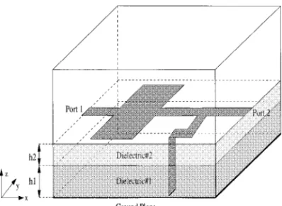
In this study, the spatial-domain MoM employ-ing subdomain basis functions is used to solve the
Ž . w x
mixed potential integral equation MPIE 7]9 for current distribution on the conductors, which are immersed in a planar layered medium, as shown in Figure 1.
Using the spatial-domain Green’s functions in the MoM for a planar layered medium requires numerical integration of Sommerfeld integrals w x10 , which is a very time consuming process. But, it was recently recognized that the Sommerfeld integrals can be approximated analytically, which provides the closed-form spatial-domain Green’s
Q 1997 John Wiley & Sons, Inc. CCC 1050-1827r97r050344-15
Figure 1. A typical printed geometry.
w x
functions 11 . With the use of these closed-form Green’s functions in conjunction with the spatial-domain MoM, the computational effi-ciency of the MoM is significantly improved for small- and moderate-size geometries. In addition, when the closed-form Green’s functions are em-ployed in the MoM, the resulting MoM matrix elements can also be evaluated analytically, which further improves the computational efficiency of
w x the technique 12 .
So far, the technique is discussed from the analysis point of view, but, in designing a printed circuit, optimization plays an important role as well. An optimization algorithm, in general, re-quires the simulation program to analyze the modified geometry at each iteration. Meanwhile, if the simulation program needs to analyze the modified geometry from scratch, the optimization algorithm would be computationally expensive even though the simulation program is efficient. Therefore, to assess the numerical efficiency of a simulation technique it is necessary to consider the suitability of the technique for optimization. The technique that we present here is very suit-able because the effects of newly added or re-moved metallic regions are handled very fast by adding an additional row]column pair to or re-moving a row]column pair from the original ma-trix for each additional basis function, respec-tively. In addition to the efficient filling of the MoM matrix of the modified geometry, the solu-tion time of the modified matrix equasolu-tion can also be improved by using the solution of the matrix equation in the previous iteration through the method known as the order recursive
Gauss-w x ian elimination approach 13 .
In the next section, application of the spatial-domain MoM to the solution of the MPIE is briefly explained from a theoretical point of view, and the use of the closed-form Green’s functions is introduced, without giving the details. Then, assuming that the surface current density is ob-tained, the de-embedding of the circuit parame-ters, such as input impedance and S-parameparame-ters, is explained. Then, in the fourth section, some practical passive MMIC components are charac-terized to illustrate the use of the proposed method, and the results are compared with those obtained from commercial EM software, em ŽSonnet Software, Inc. . The final section presents. the conclusions.
THEORETICAL BACKGROUND
The geometry of a general printed structure in a multilayer medium is shown in Figure 1. The layers are planar and assumed to be infinitely wide in the horizontal plane, and the conductors are lossless and infinitesimally thin. An ejw t time
dependence is assumed and suppressed.
The field components in a planar stratified w x
medium can be expressed as 7 : 1 A Exs yjwG ) J qx x x jw x = q Jx q Jy q Jz Ž . Gx) q G )y q G )z 1 x y z 1 A Eys yjwG ) J qy y y jw y = q Jy q Jx q Jz Ž . Gy) q G )x q G )z 2 y x z E s yjwGA) J y jwGA) J z z x x z y y 1 Jx A q y jwG ) J qz z z Gx) jw z x Jy Jz q q Ž . qG )y q G )z 3 y z
where GA and Gq are the spatial-x spatial-x, y y, z spatial-x, z z x, y, z
domain vector and scalar Green’s functions, re-spectively; J , J , J are the surface current densi-x y z ties; and ) denotes the convolution operator. Because the traditional form of the Green’s
func-w x tions are employed in the formulation 14 , the Green’s function of the scalar potential is not unique for HED and VED. Therefore, the scalar
Ž . Ž . qe qe
potentials given in eq. 1] 3 are G s G for ax y
HED and Gqe for a VED. In the application of z
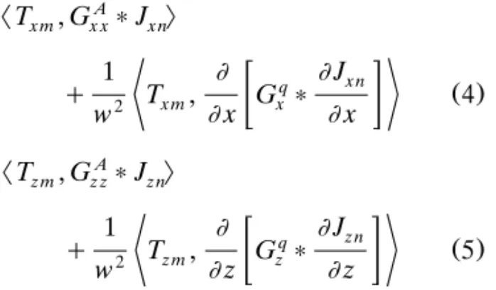
the MoM, the surface current densities are ex-panded in terms of some suitable basis functions, and the resulting field expressions are tested by a suitable class of testing functions. Here we have chosen the rooftop functions as the basis and testing functions on both horizontal and vertical conductors, resulting in Galerkin’s MoM. For the sake of illustration, the basis functions used for a typical printed geometry are shown in Figure 2. Hence, the MoM matrix equation is obtained with typical matrix entries as:
²Tx m, Gx xA) Jx n: 1 q Jx n Ž . q 2
¦
Tx m, Gx);
4 x x w ²Tz m, Gz zA) Jz n: 1 q Jz n Ž . q 2¦
Tz m, z Gz) z;
5 wwhere Tx m, Tz m and J , Jx n z n denote the testing ² : and basis functions, respectively, and , desig-nates the inner product. After solving the matrix equation, the current distributions on the conduc-tors are found and, from the current distribution, the circuit parameters can be extracted.
Ž . Ž . If the inner-product terms in eqs. 4 and 5 are examined, it is seen that the spatial-domain Green’s functions play an important role in the calculation of the inner products. This is because the spatial-domain Green’s functions are ob-tained from the spectral-domain counterparts through an integral transformation, called the Hankel transform or the Sommerfeld integral in
w x
electromagnetics 15 . This transformation is given as: 1 Ž2.Ž .
˜
Ž . Ž . GsH
dk k Hr r 0 krr G kr 6 4p SIP˜
where G and G are the Green’s functions in the spatial and spectral domains, respectively; HŽ2. is
0
the Hankel function of the second kind; and SIP is the Sommerfeld integration path. Because the aim is to eliminate the numerical integration in
Ž .
eq. 6 , the spectral-domain Green’s function is approximated by complex exponentials, whose Hankel transform can be performed analytically, resulting in closed-form spatial-domain Green’s
w x
functions 16, 17 .
The exponential approximation is performed by using the generalized pencil of function method ŽGPOF.w x18 at three steps along the path shown in Figure 3. This is an extension of the two-level
w x
approach introduced recently 17 , so the details of this approximation scheme are not included
Ž .
here one may refer to ref. 17 . However, we should note that this multilevel approach elimi-nates the need to extract the quasistatic images
Figure 3. The path used in exponential approxima-tion.
and the surface-wave poles, which further im-proves the computational efficiency of the deriva-tion of the closed-form Green’s funcderiva-tions. The reason for the extension of the two-level ap-proach to the three-level apap-proach can be ex-plained as follows: When a vertical conductor is used, such as shorting pins or via holes, the fields due to the current on this conductor have to be evaluated over a very small distance, r, requiring a very accurate approximation for large k . So,r the third region is added onto the two-level approach to give enough emphasis to the ap-proximation for large k , without increasing ther computational complexity of the whole approxi-mation. As a result of this approximation, the spectral-domain Green’s functions are obtained in the following form:
N1 N2 1 yb k yb k 1 n z 2 n z
˜
G(½
Ý
a e1 n qÝ
a e2 n j2 kz ns1 ns1 N3 yb k3 n z Ž . qÝ
a e3 n5
7 ns1Once the spectral-domain Green’s functions are represented as the sum of complex exponentials,
Ž .
each exponential term in eq. 17 can be trans-formed to the spatial domain via the Sommerfeld identity:
eyj k r 1 eyjkz< z <
Ž2.Ž . Ž .
s
H
dk k Hr r 0 krr 8r 2 j SIP kz
yielding the following Green’s function expression in the spatial domain:
N1 eyj k ri 1 n N2 eyjk ri 2 n G(
Ý
a1 n qÝ
a2 n r1 n r2 n ns1 ns1 N3 eyj k ri 3 n Ž . qÝ
a3 n 9 r3 n ns1 2 2 2 2'
'
where r1 ns r y b , r s r y b , r1 n 2 n 2 n 3 n 2 2'
2 2'
s r y b , and r s x q y . Next, the3 n
closed-form representation of the spatial-domain Ž . Green’s functions are substituted into eqs. 4 and Ž .5 and the resulting integrals, for the convolution and the inner product, are evaluated analytically as described in ref. 12. Hence, the use of the closed-form Green’s functions in the MoM re-sulted in an accurate simulation technique with no numerical integration involved, giving rise to a
very efficient and yet accurate EM simulation software.
Although the approach just described seems straightforward, it has some difficulties in cases of geometries with vertical conductors. Because the spectral domain Green’s functions are sampled for the purpose of approximation, the variables z and z9 have to be fixed to the observation and source planes, respectively. Therefore, the result-ing closed-form spatial-domain Green’s functions become valid only for these specific source and observation points. In cases of only horizontal conductors, this poses no problem because the source and observation planes are already fixed. However, in the case of a vertical conductor, eq. Ž .5 shows that one needs to integrate along z9 for the convolution integral and along z for the inner-product integral. If the technique just de-scribed is used directly, the exponential approxi-mation needs to be performed for every integra-tion point of z and z9, which would result in an extremely inefficient approach to incorporate a vertical conductor. Instead, the Green’s functions
Ž .
for the vertical electric dipole in eq. 5 are writ-ten as the inverse Hankel transform of their spectral domain representations, and the integrals on z and z9 variables are performed analytically in the spectral domain. Then, the resulting func-tions are transformed to the spatial domain as just described and the remaining integrals are evaluated analytically as before. Note that the spectral-domain Green’s functions consist of ex-ponential functions of z and z9 which permits the
w analytical integration in the spectral domain 16,
x
19 . In the approach just described, the number of basis functions selected in the z-direction is not limited; therefore, the lengths of the vertical con-ductors can be arbitrarily long.
METHOD OF DE-EMBEDDING OF PORT DISCONTINUITIES
Because there exists fringing, reactive, and evanescent fields in the vicinity of source and load terminals, circuit parameters, like input impedances and S-parameters, are obtained by removing these higher order effects from the w x calculations, which is called de-embedding 20 . The EM simulation technique presented in this
Ž .
work uses impressed current sources see Fig. 2 w x
to characterize N-port circuits 21 .
Because the current densities on the conduc-tors, including the port transmission lines, have
already been calculated, the current on each port transmission line is written as the linear combina-tion of complex exponentials by using the GPOF as follows:
N
Ž . wŽ . x Ž .
I l f
Ý
I expi a q j b li i 10is1
where l is the distance along the port transmis-sion line. If the magnitudes of higher order modes on the port transmission lines are sufficiently small, the current can be expressed by only two exponentials with complex coefficients corre-sponding to the incident and reflected current waves at the corresponding ports. Then, the S-parameters are calculated from the coefficients of these exponentials and transferred to the desired
w x
reference planes 22 . These S-parameters are inherently normalized and referenced to the char-acteristic impedances of the port transmission lines. Note that, by using this method, the propa-gation constants on the transmission lines are also found, which enables us to extract the effec-tive permittivity at each frequency of operation. However, in some cases, it might be numerically difficult to extract the propagation constant and the unknown coefficients of the exponentials with sufficient precision from the same current sam-ples by direct application of GPOF. This situation occurs in MMIC structures where the electrical length of the port transmission line is very small. In that case, one can find the propagation con-stant from a sufficiently long test transmission line which has the same characteristics as the original port transmission line, and then use this propagation constant to fit the current on the original line with complex exponentials through a
w x
linear least-squares algorithm 23 . Finally, the parameters obtained are converted to the S-parameters with the reference impedance of 50 V.
For a two-port network, the matrix relation, used to find the S-parameters, can be written in the following form:
q q y I11 I12 0 0 S11 yI11 q q y 0 0 I11 I12 S12 yI12 Ž . s 11 q q y I21 I22 0 0 S21 yI21 q q S y 0 0 I21 I22 22 yI22
where Iqi j and Iyi j are the current coefficients for incident and reflected waves, respectively, for ith port excitation and jth port observation. Note that, in calculating the S-parameters, it is not
necessary to terminate the ports because, both the transmitted and reflected waves are consid-ered in the calculations. To calculate the S-parameters of a general N-port network with characteristic impedances Z0i at port i, the fol-lowing pseudo-code, which fills the matrices in eq. Ž11 , is given here for convenience:.
A¤ 0 n¤ number of ports for is 0, 1, 2, . . . , n y 1 begin for ls 0, 1, 2, . . . , n y 1 begin for ms 0, 1, 2, . . . , n y 1 begin q Ž . Ai) nqm, lqm) n¤ I )sqrt Zi l 0l end y Ž . Bi) nql¤ yI )sqrt Zi l 0l end end
Note that this derivation of the S-parameters does not require the knowledge of the character-istic impedances of the port transmission lines. However, the need to convert these S-parameters to the S-parameters with a known reference
Ž .
impedance usually 50 V makes it necessary to know the characteristic impedances of the port transmission lines. Because a rigorous calculation of the characteristic impedance of a microstrip line in a multilayer medium is quite time consum-ing, a method based on a quasi-TEM approach is used here, which provides a closed-form expres-sion for the characteristic impedance of a
mi-w x
crostrip line and a stripline 24, 25 . This method is valid when the transverse components of the current densities on the port transmission lines are very small as compared with the longitudinal components, which is usually the case for MMICs. Note that the characteristic impedance found from the quasi-TEM approach does not change with frequency, whereas, in reality, it changes
w x
with frequency 26, 27 . By using a frequency-dependent effective permittivity in the closed-form expression for the characteristic impedance, the quasi-TEM approximation is somewhat ex-tended.
EXAMPLES
In this section, some examples are given and the results are compared with those obtained from
Ž .
Ž . Figure 4. Geometry of the hybrid coupler showing the ports not to scale .
w x
Carroll and Chang 28 for general information on em software. The first three examples are the structures which have multilayer metalization, and the last example is a microstrip line with a shunt short-circuited stub to demonstrate the use of the vertical connection. The S-parameters provided here are normalized with respect to 50-V refer-ence impedance.
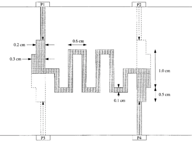
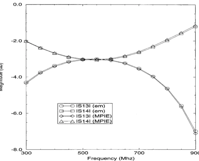
As a first example, a multilayer 3-dB 908 hybrid coupler is analyzed. The geometry and layer in-formation of the coupler are given in Figures 4 and 5, respectively. The results obtained from the method presented in this article show very good agreement with the results obtained with em
soft-Ž .
ware Figs. 6 and 7 .
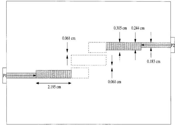
The next example is a coupled-line band-pass filter whose geometry and layer information are given in Figures 8 and 9, respectively. In design-ing edge-coupled filters, it might be necessary to have small spacings}in other words, large cou-plings, between the resonant elements, which would make the production of such filters very difficult. This difficulty can be circumvented by implementing such coupled lines in a stripline
w x
geometry with broadside coupling 29, 30 . Here, by using this concept, a third-order band-pass filter is designed by following the design proce-dure based on the even- and odd-mode impedances of the coupled lines, which are
avail-w x
able in the literature 25 . The analysis of this
Figure 6. Magnitudes of S13and S14of the hybrid coupler shown in Figure 4.
Ž . Figure 8. Geometry of the band-pass filter showing the ports not to scale .
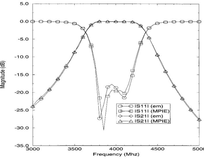
filter is performed by using the method described here and by the em software, and the results are in perfect agreement, as shown in Figure 10 and 11. Note that the response of the filter can be further improved without substantially increasing the computation time by using a fully automated optimization algorithm.
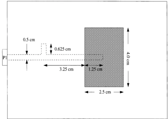
Another example is a proximity-coupled mi-crostrip patch antenna, whose geometry and layer information are given in Figures 12 and 13, re-spectively. Because the major disadvantage of mi-crostrip antennas is the small bandwidth, this can
be improved by using a proximity-coupled feed w x
structure 31 , as shown in Figure 12. Note that a tuning stub at the feeding line is used to match the antenna to the characteristic impedance of the line. Here, the antenna is analyzed with and without the tuning stub with reference planes at the stub position and at the antenna edge, respec-tively, and the results are provided in Figures 14 and 15. It should be noted that the analysis of a radiating structure by using em requires some conditions to be satisfied: namely, the size of the box must be increased, the top cover must be
Figure 10. Magnitudes of S11and S21of the band-pass filter shown in Figure 8.
Figure 12. Geometry of the proximity-coupled microstrip antenna showing the input port Žnot to scale ..
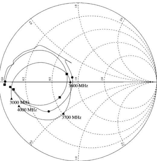
terminated in 377 V, and the free space above the structure should be made slightly lossy. Even then, the results obtained show some artifacts ŽFig. 14 , and the computation time increases. significantly because of the increased number of unknown for the larger box. The results obtained by the approach presented in this article agree quite well with the results obtained from the em software, except the artifacts, but there is a slight shift in the position of the experimental curve
that could be attributed to de-embedding of the experimental data.
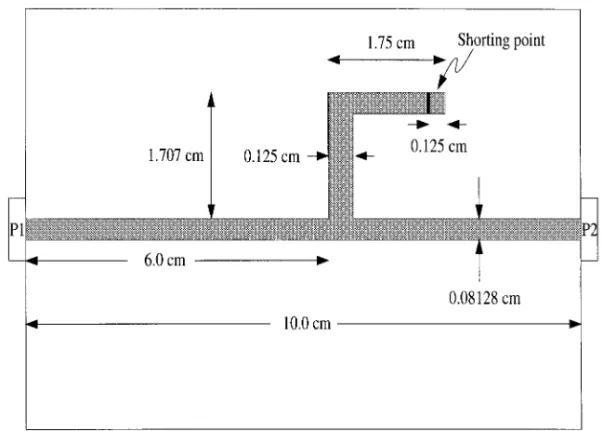
Finally, a microstrip line with a
shunt-short-Ž .
circuited stub Fig. 16 is analyzed. The thickness
Ž .
of the substrate is 0.02032 cm s 8 mils , and « s 4. It should be noted that the use of vias orr
shorting pins in the em software has some restric-Ž .
tions: i the assumption of uniform current distri-Ž . bution along the vertical connection; and ii limi-tation on the length of the vertical conductor
Figure 13. Layer information for the proximity-coupled microstrip antenna shown in Figure 12.
Figure 14. G of the proximity-coupled microstrip antenna shown in Figure 12 withouti n
Ž w x.
tuning stub square: MPIE; circle: em; triangle: measured 31 .
Figure 15. G of the proximity-coupled microstrip antenna shown in Figure 12 with tuningi n
Ž w x.
Ž . Figure 16. Geometry of a short-circuited microstrip line showing the ports not to scale .
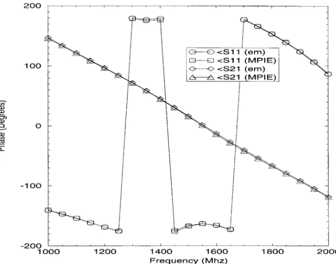
Figure 18. Phases of S11and S21of the microstrip line shown in Figure 16.
Žsmall fraction of a wavelength . On the other. hand, the method presented here has no such restrictions, and can handle any length of the vertical conductors with the rooftop basis func-tions to represent the current. The results ob-tained from both methods are shown in Figures 17 and 18, and they are in good agreement for this very short shorting pin.
CONCLUSIONS
In this article, we have presented an efficient and accurate technique for EM simulations of printed geometries in multilayer media. The technique is based on the spatial-domain MoM used with the closed-form Green’s functions. It was applied to some printed geometries, and it was demon-strated that the results obtained are in good agreement with the results obtained from a pro-fessional electromagnetic analysis software. The advantages of this technique can be stated as
Ž . Ž .
follows: i it is very suitable for optimization; ii Ž . it can handle radiating structures efficiently; iii the vertical connections with arbitrary lengths can
Ž .
be easily modeled: and iv it has the potential of
being the most efficient EM software for passive MMIC components.
REFERENCES
1. P. Silvester and P. Benedek, ‘‘Equivalent Capaci-tance of Microstrip Open Circuits,’’ IEEE Trans.
Microwa¨e Theory Tech., Vol. MTT-20, August 1972,
pp. 511]516.
2. P. Benedek and P. Silvester, ‘‘Equivalent Capaci-tance of Microstrip Gaps and Steps,’’ IEEE Trans.
Microwa¨e Theory Tech., Vol. MTT-20, November
1972, pp. 729]733.
3. P. Silvester and P. Benedek, ‘‘Equivalent Disconti-nuities Capacitances for Right-Angle Bends,
T-junctions, and Crossins,’’ IEEE Trans. Microwa¨e
Theory Tech., Vol. MTT-21, May 1973, pp. 341]346.
4. R. F. Harrington, Field Computations by Moment
Methods. Macmillan, New York, 1968.
5. J. Jin, The Finite Element Method in
Electromagnet-ics. John Wiley, New York, 1993.
6. K. Kunz and R. Luebber, The Finite Difference
Time Domain Method for Electromagnetics. CRC
Press, Boca Raton, FL, 1993.
7. J. R. Mosig, ‘‘Arbitrarily Shaped Microstrip Struc-tures and Their Analysis with a Mixed Potential
Integral Equation,’’ IEEE Trans. Microwa¨e Theory Tech., Vol. MTT-36, February 1988, pp. 314]323.
8. I. Park, R. Mittra, and M. I. Aksun, ‘‘Numerically Efficient Analysis of Planar Microstrip Configura-tions Using Closed-form Green’s funcConfigura-tions,’’ IEEE
Trans. Microwa¨e Theory Tech., Vol. 43, February
1995, pp. 394]400.
9. K. A. Michalski and Juan R. Mosig, ‘‘Discrete Complex Image MPIE Analysis of Coax-Fed Cou-pled Vertical Monopoles in Grounded Dielectric Substrate: Two Formulations,’’ IEE Proc.
Mi-crowa¨e Ant. Propagat., Vol. 142, June 1995, pp.
269]274.
10. J. R. Mosig and F. E. Gardiol, ‘‘Analytical and Numerical Techniques in the Green’s Function Treatment of Microstrip Antennas and Scatters,’’
IEE Proc., Vol. 130, March 1983, pp. 175]182.
11. Y. L. Chow, J. J. Yang, D. G. Fang, and G. E. Howard, ‘‘A Closed-Form Spatial Green’s Function for the Thick Microstrip Substrate,’’ IEEE Trans.
Microwa¨e Theory Tech., Vol. 39, March 1991, pp.
588]592.
12. L. Alatan, M. I. Aksun, K. Mahadevan, and T. Birand, ‘‘Analytical Evaluation of the MoM Matrix
Elements,’’ IEEE Trans. Microwa¨e Theory Tech.,
Vol. 44, April 1996, pp. 519]525.
13. K. Naishadham and P. Misra, ‘‘Order Recursive Gaussian Elimination and Efficient CAD of Mi-crowave Circuits,’’ IEEE MTT-S Dig., 1995, pp. 1435]1438.
14. K. A. Michalski and Dalian Zheng, ‘‘Electromag-netic Scattering and Radiation by Surfaces of Arbi-trary Shape in Layered Media, Part I: Theory,’’
IEEE Trans. Ant. Propagat., Vol. AP-38, March
1990, pp. 335]344.
15. A. Sommerfeld, Partial Differential Equations in
Physics. Academic Press, New York, 1949.
16. G. Dural and M. I. Aksun, ‘‘Closed-Form Green’s Functions for General Sources and Stratified Me-dia,’’ IEEE Trans. Microwa¨e Theory Tech., Vol. 43, July 1995, pp. 1545]1552.
17. M. I. Aksun, ‘‘A Robust Approach for the Deriva-tion of Closed-Form Green’s FuncDeriva-tions,’’ IEEE
Trans. Microwa¨e Theory Tech., Vol. 44, May 1996,
pp. 651]658.
18. Y. Hua and T. K. Sarkar, ‘‘Generalized Pencil-of-Function Method for Extracting Poles of an EM
System from Its Transient Response,’’ IEEE Trans.
Ant. Propagat., Vol. AP-37, February 1989, pp.
229]234.
19. W. C. Chew, Wa¨es and Fields in Inhomogeneous
Media. Van Nostrand Reinhold, New York, 1990.
20. J. C. Rautio, ‘‘A De-Embedding Algorithm for Electromagnetics,’’ Int. J. MIMICAE, Vol. 1, 1991, pp. 282]287.
21. G. V. Eleftheriades and J. R. Mosig, ‘‘On the Network Characterization of Planar Passive Cir-cuits Using the Method of Moments,’’ IEEE Trans.
Microwa¨e Theory Tech., Vol. 44, March 1996, pp.
438]445.
22. T. K. Sarkar, Z. A. Maricevic, and M. Kahrizi, ‘‘An Accurate De-Embedding Procedure for Character-izing Discontinuities,’’ Int. J. MIMICAE, Vol. 2, 1992, pp. 135]143.
23. R. Kipp and C. H. Chan, ‘‘Triangular-Domain Ba-sis Functions for Full-Wave AnalyBa-sis of Microstrip
Discontinuities,’’ IEEE Trans. Microwa¨e Theory
Tech., Vol. 41, JunerJuly 1993, pp. 1187]194.
24. F. Gardiol, Microstrip Circuits. Wiley, New York, 1994.
25. H. Howe, Jr. Stripline Circuit Design. Artech House. Dedham, MA, 1974.
26. K. C. Gupta, R. Garg, and I. J. Bahl, Microstrip
Lines and Slotlines. Artech House, Dedham, MA,
1979.
27. J. C. Rautio, ‘‘A New Definition of Characteristic Impedance,’’ IEEE MTT-S Dig., 1991, pp. 761]764. 28. J. Mason Carroll and K. Chang, ‘‘Full-Wave Con-vergence Analysis of Microstrip Transmission Pa-rameters,’’ Int. J. MIMICAE, Vol. 4, April 1994, pp. 140]147.
29. B. Bhat and S. K. Koul, Stripline-Like Transmis-sion Lines for Microwave Integrated Circuits. Wi-ley, Chichester, UK, 1989.
30. W. Schwab, F. Boegelsack, and W. Menzel, ‘‘Multi-layer Suspended Stripline and Coplanar Line
Fil-ters,’’ IEEE Trans. Microwa¨e Theory Tech., Vol.
MTT-42, July 1994, pp. 1403]1407.
31. D. M. Pozar and B. Kaufman, ‘‘Increasing the Bandwidth of a Microstrip Antenna by Proximity Coupling,’’ Electron. Lett., Vol. 23, April 1987, pp. 368]369.
BIOGRAPHIES
Noyan Kınayman received the BSc and MSc degrees, both in
electrical and electronic engineering, from Middle East
Tech-Ž .
nical University METU , Ankara, Turkey, in 1990 and 1993, respectively. During the period from June 28, 1990 to Septem-ber 1, 1994, he worked in the Department of Preparation to Production, Aselsan Military Electronics Inc., as a design and
test engineer. His major duty was to design computer-con-trolled and manual RF test systems which are used on the tests of various military and nonmilitary radios. In October 1994, he joined the EE Department of Bilkent University as a research assistant. His major professional interest is numerical
Ž .
M. I. Aksun received the BS and MS degrees in electrical and
electronics engineering from the Middle East Technical Uni-versity, Ankara, Turkey, in 1981 and 1983, respectively, and the PhD degree in electrical and computer engineering from the University of Illinois at Urbana-Champaign in 1990. From 1990 to 1992, he was a postdoctoral fellow at the Electro-magnetic Communications Laboratory, University of Illinois
Urbana-Champaign. Since 1992, he has been on the faculty of the Department of Electrical and Electronics Engineering at Bilkent University, Ankara, Turkey, where he is currently an associate professor. His research interests include numerical methods for electromagnetics, microstrip antennas, and
mi-Ž
crowave and millimeter-wave integrated circuits. Photo not .