•-■»íií,·-·· ¡"'κΰ ?^ı?ö ;?'.' ^ - • ^ ' - 1·^ U ^ .C iJ w i - i - 1 v i w U - ίί -'■■* j ■ • w 'i V ч і 'і і ί*4ι fiu^ ■»¿'w .A «,. ·* - - . -Л :.v,ίϊ- » 1 і!<»М М Ç- ¿fc y·«· í;·* і""'>1..'':ч’ѵ l ^ Ü i v W *.■'-J ... ч«-> .. ' S v íí ' w ·. -V .'.;-·».^ Г К
Z 5 H
’ £ MDESIGN AND IMPLEMENTATION OE A DSP BASED
CONTROLLER FOR BRUSHLESS DC MOTORS
A THESIS
SUBMITTED TO THE DEPARTMENT OF ELECTRICAL AND ELECTRONICS ENGINEERING
AND THE INSTITUTE OF ENGINEERING AND SCIENCES OF BILKENT UNIVERSITY
IN PARTIAL FULFILLMENT OF THE REQUIREMENTS FOR THE DEGREE OF
MASTER OF SCIENCE
By
Armagan E R G U N November 1996 ArrtVi^QA £rgui/l . icrafmdan bcj^i^lcnmi^Ur^ßC36282
τ κ
I certif}'^ that I have read this thesis and that in opinion it is fully adequate, in scope and in quality, as a thesis for the degree of Master of Science.
Assoc. Prof. Dr. Ö. Morgül(Supervisor)
1 certify that I have read this thesis and that in my opinion it is fully adequate, in scoi^e and in quality, as a thesis for the degree of Master of Science.
Assoc. Prof. Dr. Billur Barshan
I certify that I have read this thesis and that in my opinion it is fully adequate, in scope and in quality, as a thesis for the degree of Master of Science.
Approved for the Institute of Engineering and Sciences:
Prof. Dr. Mehmet B d^ y
ABSTRACT
DESIGN AND IMPLEMENTATION OF A DSP BASED
CONTROLLER FOR BRUSHLESS DC MOTORS
Arm ağan ER G Ü N
M .S . in Electrical and Electronics Engineering Supervisor: Assoc. Prof. Dr. O. Morgiil
November 1996
This work presents development of a high speed digital signal processor based controller for Brushless DC Motors. A working model of the plant as motor and amplifier is introduced and verified through experiment. Design and implementation of the hardware using wire-wrap board is accomplished and a PID control algorithm is developed. A user interface is designed for easy performance testing of the control system.
ÖZET
S A Y IS A L s i n y a l İŞL E M C İL İ B İR F IR Ç A S IZ M O T O R
D E N E T L E Y İC İ T A S A R IM I V E U Y G U L A N M A S I
Arm ağan E R G Ü N
Elektrik ve Elektronik Mühendisliği Bölümü Yüksek Lisans Tez Yöneticisi: Assoc. Prof. Dr. O. Morgül
Ekim 1996
Bu tezde, yüksek hızlı bir sayısal sinyal işlemci kullanarak fırçasız bir motor için denetleyici geliştiriliTiiştir. Motor ve sürücü olarak sistemin bir modeli oluşturulmuş ve deneylerle ispatlanmıştır. İsteklere uygun bir kontrol kartı ve kontrol algoritması tasarlanmıştır. Denetleyicinin performansını kolay bir şekilde değerlendirebilmek için kullanici ara birimi geliştirilmiştir.
Anahtar Kelimeler : Motor kontrolü, Sayısal sinyal işlemcileri. Yüksek hızlı denetleyiciler
ACKNOWLEDGMENTS
I would like to thank to Assoc. Prof. Dr. 0 . Morgiil for his supervi sion, guidance, suggestions and encouragement through the development of this thesis.
I would also like to thank to Assoc. Prof. Dr. Billur Barshan and Prof. Dr. Hayrettin Koymen for reading and commenting on the thesis.
It is a pleasure to express my thanks to all my collègues at TUBITAK-SAGE for their valuable discussions and helps. TUBITAK-SAGE, who supported this work is greatly acknowledged.
Contents
1 Introduction 7
2 BRUSHLESS DC M OTORS A N D AMPLIFIERS 11
2.1 Introduction to Brushless System s... 11 2.2 Advantages of Brushless DC M o to rs... 12
2.-3 Operation of Brushless DC Motors 14
2.4 Operation of the A m p lifier... 16
3 MODELLING OF THE BRUSHLESS M O T O R AND A M P LI
FIER USING SPICE 23
3.1 Model of the Brushless M o t o r ... 23
3.2 Model of the Brushless Amplifier 28
3.3 S im u la tio n s... 29
4 DESIGN OF THE POSITION CONTROLLER 34
4.1 Simplification of the motor m o d e l ... 34
4.2 Simplification of the amplifier model 36
4.3 Controller D e s ig n ... 39
4.4 Implementation of BID controller on DSP 42
4.4.1 Modification and D iscretiza tion ... 42
4.4.2 Implementation Issues 47
5.1 Digital Signal Processor 49
5.2 Memory 51
5.3 Digital to Analog Conversion 53
5.4 Encoder P rocessin g... 55 5.5 Serial P o r t ... 57
5.6 Dual Port Memory 59
5.7 P r o t o t }q )e ... 60
6 Software Design 61
6.1 Assembly C o d e ... 61
6.1.1 The Monitor Program 62
6.1.2 The Control A lgorith m ... 66 6.2 Visual Basic User Interface... 67
7 Experimental Verification 69
List of Figures
1-1 Digital Control S y s te m ... 8 1- 2 S}'stem O v e r v ie w ... 9
2- 1 Conventional DC Motor 11
2-2 Alternating voltage appearing on the terminals... 15 2-3 T3q3ical Brushless Motor wound with 3 P h a s e s ... 16 2-4 Simplified Block Diagram of the PWM Amplifier 17 2-5 Simplified Pulse Width M odulator... 18 2-6 Configuration of the Switching Power Amplifier 19 2- 7 Hall effect device ou tp u ts... 20
3- 1 Schematic drawing of the electrical part of the motor 27 3-2 Schematic Drawing of the Mechanical Part of the Motor 27 3-3 Truth Table and reduced Logic Equations of Switching Amplifier . 28 3-4 Shaft Speed Graph for Short Term Simulations 30 3-5 Shaft Angle Graph for Short Term S im u la tion ... 30 3-6 Phase Currents for Short Term S im u la tion ... 31 3-7 PW M and Feedback Signals for Short Term S im u lation ... 32
3-8 Shaft Speed Graph for Long Term Simulation 32
3- 9 Shaft Angle Graph for Long Term Sim ulations... 33
4- 1 Brush type motor m o d e l ... 34 4-2 Simplified motor m o d e l... 35
4-3 Phase Generating C ircu it... 36
4-4 Continuous current m o d e ... 36
4-5 H-t5'pe PW M am plifier... 37
4-6 Block diagram of the simplified amplifier and m o t o r ... 38
4-7 Simplified position control s y s te m ... 39
4-8 Poles of the Closed Loop System 40 4-9 Step Responses of the Open and Closed Loop S y s te m ... 42
4- 10 Structure of the PID C o n tr o lle r ... 46
5- 1 System Block D ia g r a m ... 49
5-2 Memory Block Diagram 51 5-3 DAC Block D ia g r a m ... 54
5-4 Bipolar Code Table 55 5-5 Encoder Output W a v e fo rm s ... 55
5-6 Encoder Processing Block D ia g r a m ... 56
5-7 State Diagram of E - P A L ... 57
5-8 Serial Port Block D ia g r a m ... 58
5- 9 Dual Port Memory Block Diagram 60 6- 1 Timing of Software F u n c t io n s ... 62
6- 2 Flowchart for Monitor P r o g r a m ... 63
7- 1 Open Loop Step Response of the System (Motor and Amplifier) 70 7-2 Step Response of the Closed Loop System for Step Input of 50 d egrees... 71
7-3 Error Plot between the Experimental and MATLAB Step Re sponses for Step input of 50 d egrees... 71
7-4 Position Error for the Experiment shown in Figure 7.2 72 7-5 Step Response of the Closed Loop System for Step Input of 30 d egrees... 73
7-6 Experiment showing the position response of the system for suc
List of Tables
2.1 .Six Sequence Commutation 21
5.1 Output Port M a p ... 50 5.2 Input Port M a p ... 51 5.3 Memory Map: BO as Data M e m o r y ... 53
Chapter 1
Introduction
Control systems are a necessary part of modern manufacturing, industrial pro cesses, and our daily lives. They range from simple control systems like those on air conditioning to more intricate control systems like those for a missile guid ance system. Control mechanism ha.ve evolved from mechanical, pneumatic, and electromechanical systems to electronic control systems. Electronic control sys tems ha.ve been implemented with analog components like resistors, capacitors and op-amps. However, with the availability of microprocessors, control systems cire being implemented in digital form. The use of microprocessors in digita.l control systems has created not only some new opportunities due to the power ful processing capabilities of microprocessors, but also a need for a. new body of knowledge that utilizes some of these processing capabilities.
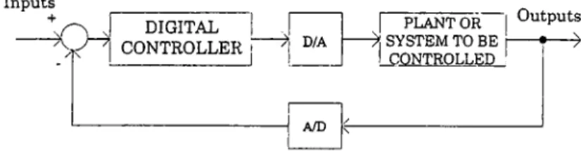
A digital controller is a signal processing system that executes algebraic al gorithms inherent to the control of feedback systems. Together with the plant (system to be controlled) and signal acquisition circuitry, the digital controller makes up a digital control system such as the one shown in Figure ( T l) .
Note that this system requires analog-to-digital (A /D ) converters to trans form the analog output signals of the plant to digital signals for the input of the controller. The system also requires a digital-to-a.nalog (D /A ) converter to
transform the digital output signals of the controller to analog signals for the input of the plant.
Inputs + DIGITAL I , I CONTROLLER i A/D PLANT OR SYSTEM TO BE I
I
CONTROLLED ' ^— I OutputsFigure 1-1; Digital Control Sj'stem
The advantages of the digital control approach over the analog approach are:
1. Abilit)'· to implement advanced control algorithms with software rather than special purpose hardware.
2. Ability to change the design without changing the hardware.
3. Reduced size, weight, and power, along with low cost.
4. Greater reliabilit}^, maintainability, and testability.
5. Increased noise immunit}'.
Choosing an appropriate microprocessor is an important fa.ctor in efficiently implementing a digital control design. A class of special-purpose (as opposed to general purpose) digital signal-processing microprocessors has been developed to enable fast execution of digital control algorithms. The Texas Instruments TMS320C25 provides several beneficial features for implementing digital control system elements through its architecture, speed, and instruction set.
A prominent feature of the TMS320C25 is the on-chip 16 x 16-bit multiplier that performs two’s-complement multiplication and produces a 32-bit product
in a single 100-ns instruction cycle. The TMS320C25 instruction set includes special instructions necessary for fast implementation of sum-of-products com putations encountered in digital filtering/compensation and Fourier transform calculations. Most of the instructions critical to signal processing are executed in one instruction cycle.
In this thesis the requirement is to control the position of a brushless DC motor with a bandwidth of 20 Hz and position accuracy of 0.1 degrees in the range of
±6
·7T
radians. The overshoot of the control system has to be less than 10 %. The block diagram of the system is shown in Figure(l-2).Data & Power Bus Control Logic & Interace Circuits up/down increments Encoder excitaton d Position Controller & Encoder Processing
Position Command Current Command
Figure 1-2; System Overview
This svstem consists of:
• DC-Brushless Motor with incremental Encoder
• Power Amplifier for excitation of DC-Brushless Motor
• Position Control Loops with Encoder Processing implemented with TMS320C25
The primary design goal for the system architecture presented in the following sections is that the controller should provide enough processing power to accom modate advanced control algorithms. A specific statement of that goal is that the system should be able to execute one full loop of position control algorithm within 200/rs. This goal was to be achieved while retaining a feasible single pro cessor architecture. The secondary design goal for the system is an easy and flexible motor drive interface.
The goals of the system design forced the following decisions to be made about specifications for the DSP and the input/output hardware. The instruction cycle of the DSP should be 100-ns or lower. The system should have fast memory to execute program code with no wait-states. The decoding of position encoder outputs .should be implemented in hardware, as the use of the DSP and interrupts for this task would consume a significant portion of the processing time when the motor drive runs at high rotational speeds. For flexibility, the system should easily interface with both major types of position encoder.
The thesis is organized as follows. Chapter 2 contains a discussion of the brushless motors and their amplifiers with their operations. Chapter 3 intro duces a SPICE model for the motor and amplifier as a plant to be controlled. Chapter 4 deals with the design of the control algorithm and simplification of the plant model. Chapter 5 contains a discussion of each major section of the hardware design. Chapter 6 describes and gives examples of software to support all the hardware features of the system. Chapter 7 discusses the experimental verification of the system. Conclusions are presented in Chapter 8.
Chapter 2
B R U SH LESS D C M O T O R S
A N D A M P L IF IE R S
2.1
Introduction to Brushless Systems
The key to understanding and using brushless DC motor and amplifier systems is commutation: applying the power supply bus voltage in the proper sequence and at the proper time and controlling the motor current during motor operation.
Figure 2-1: Conventional DC Motor
A simple conventional DC brush motor (Figure 2-1) consists of a rotor which can turn within a magnetic field provided by the stator. If the coil connections were to be made through slip rings, this motor would behave like a step motor and
reversing the current in the rotor would cause it to flip through 180°. By including the commutator and brushes, the reversal of current is made automatically and the rotor continues to turn in the same direction.
To turn this motor into a brushless design, we must start by eliminating the windings on the rotor. This can be achieved by turning the motor insideout. In other words we make the permanent magnet as the rotating part of the motor and put the windings on the stator poles. However, we need some means of reversing the current automatically. In a servo application we will use an electronic ampli fier or drive, so commutation can be performed b}^ using the low-level signals of an Hall-effect sensor. So unlike the DC brush motor, the brushless version cannot be driven by simply connecting it up to a. source of direct current. The current in external circuit must be reversed at defined rotor positions, and the motor is in fact being driven by an alternating current.
On the surface, the concept is simple: replace the brushes and commutator bars of the familiar brush-type DC torque motor with solid-state sensors and switches. Implementation of a reliable system, however, is a greater challenge.
2.2
Advantages of Brushless DC Motors
Brushless motors offer wide advantages in control applications. The absence of brushes provides an increased reliability for brushless DC motors. High speed op eration of brush tj'pe motors is limited by arcing across commutators. Brushless motors are capable of higher speed operation.
The major advantages of the brushless motors are:
1. Since commutation is performed in circuit elements external to the rotating parts,there are no items which would suffer from mechanical wear. The brushless DC motor will, therefore, have a life expectancy limited only by mechanical bearing wear, and the reliability of the electronic controller.
2. Brushless DC motors provides the absence of brushes which generate Elec tro Magnetic Interface (EMI) noise and spark. In explosive environments or for equipment sensitive to EMI this is a considerable a.dvantage.
3. Since the heating losses are in the shell, the thermal resistance from the windings to ambient in a brushless motor is less than that of a conventional brush-t5'pe DC motor. This means higher currents are possible for the same winding temperature for a brushless motor.
4. The advances of the state-of-the-art magnetical materials have made it possible to design brushless DC motors which have very high torque-to- inertia ratios.
5. The brushless DC motors can be controlled with very efficient amplifier configurations. In cases of severe environmental conditions the controller can be located remotely from the motor. The control system can easily interface with digital and analog inputs, and is therefore well suited for incremental motion.
The brushless DC motor controller has, in general a more conq^lex configu ration than the controller for an equivalent conventional DC motor, but may be similar in size and complexity to a closed-loop step motor controller. Step motors are very useful and economical. The designer only has to specify a given number of steps. Step motors can be used efficiently as long as the load moment of in ertia and friction levels are within design limits, and the step rate is within the capability of the motor and controller. The brushless DC motor has no inherent capability of moving in discrete steps. However, with the addition of very few parts the brushless DC motor can perform better than step motors in incremental motion systems.
2.3
Operation of Brushless DC Motors
A brushless DC motor has three elements: a fixed, wound member (stator), a rotor with permanent magnets attached to it and a means of sensing rotor position. To understand how these elements work as a motor, consider some elementary magnetics.
When a current-carrying wire is placed in a magnetic field such that the cur rent fiow is perpendicular to the direction of the field, a force is exerted between the field producing element (in this case, a permanent magnet) and the wire. This force is the product of the strength of the field, the length of the wire and the current in the wire:
F = IIB (2.1)
The direction of the force will depend on the orientation of the magnetic field and the direction of the current in the wire. If the wire is disconnected from the current source and the field is moved in a direction perpendicular to the wire (so that the lines of magnetic flux cut the wire), a voltage may be measured across the ends of the wire. The magnitude of the voltage, E, depends on the flux density, B, the length of the wire, 1, and the velocity, v, with which the wire is moved through the field, or
E = Blv (2/2)
The force on the conductor in the magnetic field can be controlled by changes in B, 1 or I. In motor design, B is affected by the type of permanent-magnet material and magnetic circuit design, 1 is affected by the length and number of active conductors, and I is the total current. If the current source is removed and the rotor turned, an alternating voltage will appear across the terminals as shown in Figure 2-2. The alternating volta.ge results from the change in magnetic
polarity as the rotor turns. The amplitude and frequency of the voltage depend on the speed of rotation.
Figure 2-2: Alternating voltage appearing on the terminals
The torque produced by a motor with a given winding and physical geometry is directly related to the voltage it produces when the rotor is externally driven, or when the motor is used as a generator. In fact, the motor torque constant, Ky, and the motor voltage or back EMF constant, K^, are equal when K r is expressed in newton-meters per ampere and Kb is expressed in volts per radian
per second:
Kt = KB (2.3)
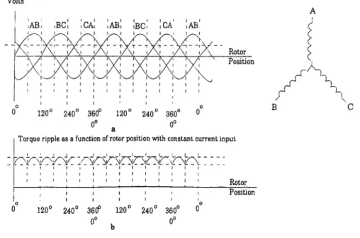
Figure 2-3 schematically shows a typical brushless motor wound with three phases and the voltages seen between the phases when the motor is run as a gen erator at constant speed. Note that the motor is wound to provide overlapping, sinusoidal 3-phase voltages, electrically spaced 120° apart. In this example, since the motor has two poles, the electrical degrees equal to mechanical degrees; that is, the electrical spacing of the phase voltages corresponds to the rotor’s physical position.
Volts
A
Torque ripple as a function of rotor position with constant current input
' : : : :
I I I I Rotor Position
0 120° 240° 360^ 120° 240° 360° 0
0° , 0°
Figure 2-3: Typical Brushless Motor wound with 3 Phases
2.4
Operation of the Amplifier
An amplifier is needed to control the power delivered to the motor and ultimately to control the system. In a brushless amplifier additional circuitry is required to electronically commutate amplifier power to the motor windings so that rotation can occur. Amplifiers coordinate various feedback signals with the command in put signals and adjust the power output level to the motor. A brushless amplifier will provide electronic commutation, feedback and command signal comparison, and the power amplification needed for brushless system control.
Commutation circuitry switches power to the different motor windings in a way analogous to a conventional motor’s brushes and commutators. Commu tation circuitry relies on rotor position information from Hall effect devices or resolvers to switch power between motor windings at the proper time.
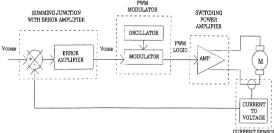
Com-mutation sensors are located about the motor axis of rotation, and the.y are electrically connected to the terminals of the amplifier. A block diagram of a basic pulse width modulation (PW M ) amplifier for a brushless motor configured for current loop operation is shown in Figure 2-4.
SUMMING JUNCTION
PWM
MODULATOR SWITCHING
Figure 2-4: Simplified Block Diagram of the PWM Amplifier
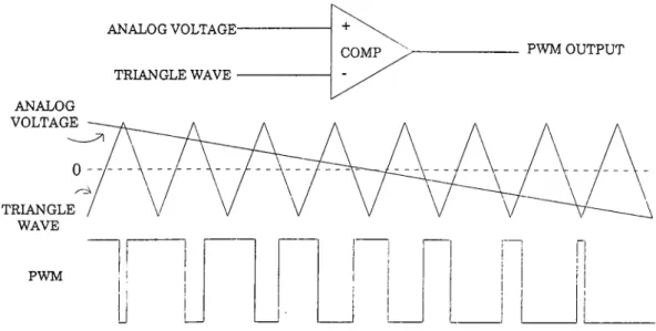
Pulse width modulation is a technique of controlling voltage applied to a load so that the amplifier power transistors always operate in a full on or full off state. The advantage of this technique is that power dissipation in the transistors is minimized. A simplified pulse width modulator is shown in Figure 2-5. The figure includes a voltage comparator which receives the analog correctional voltage on its non-inverting input and a constant frequency triangle wave on its inverting input. In operation, the analog voltage is compared to the constant frequenc}' triangle wave. When the analog voltage exceeds the triangle wave voltage, the output of the comparator is high. But, when the analog voltage is less than the triangle wave voltage, the output of the comparator is low. The result is a constant frequency, variable duty cycle pulse train generated at the output of the comparator.
ANALOG
VOLTAGE-TRIANGLE WAVE ANALOG
PWM
PWM OUTPUT
Figure 2-5; Simplified Pulse Width Modulator
The comparator duty cycle is defined as the percentage of time that the output of the comparator is high with respect to the period. So, the duty cycle is proportional to the analog correctional voltage. As the analog voltage becomes more positive, the duty cycle increases, and as the analog voltage becomes more negative, the duty cycle decreases. The resulting pulse modulation is sent to the switching power amplifier.
The switching power amplifier consists of six MOSFET switches arranged as shown in Figure 2-6. This configuration is commonly referred to as an H bridge. When switches 1 and 5 are on while others are off -f Vsupp/y is applied to phase C. When switches 2 and 4 are on while others are off -Vsupply is applied to the phase C. These switching states are called state 1 and state 2, respectively. This scheme will be applied to other phases as well. The output of the PW M modulator is used to switch the power amplifier between statel and state 2. Switching amplifier between states 1 and 2 regulates the effective voltage and current output to the
motor.
+V supply
SWITCH 1
SWITCH n i SWITCH , ! SWITCH ' ft K-| '~i I V .upply (REF) PHASE C
<
PHASE A PHASE B IFigure 2-6; Configura.tion of the Switching Power Amplifier
In general, the best position for commutation is that point at which the back EMF waveform is centered between commutation points. Commutating at the zero crossing of the back EMF waveform is ineffective since there is no resultant torque no matter how much current is applied to the phase. Peak torque per unit current for a running motor is achieved at the peak of the back EMF wa.veform.
There are two means of commutation: 6-step (or square-wave or trapezoidal) and sinusoidal (or sinewave). Six-step is simpler to implement and is used in this work. Six sequence commutation takes advantage of the three phases as shown in Figure 2-7a. Looking from left to right, a positive or negative pea.k occurs in one of the phases in every 60 electrical degrees: positive peak in phase A, negative peak in phase C, positive peak in phase B, negative peak in phase A, positive peak in phase C, and negative peak in phase B. These 60 degree ranges then repeat as the motor is rotated in the same direction. Each phase has a positive and negative 60 electrical degree operating range containing a peak. Each of the six ranges represents the optimum rotor .position for application of current to that phase to produce torque.
Reversing voltage and current polarity into the three negative ojDerating ranges will produce torque in the same direction. Figure 2-7b illustrates the resulting continuous rotating torque. The correct sequencing of phase current into the six operating ranges to provide continuous rotating torque is called the six sequence commutation method. Current is switched to each phase in this sequence with polarity indicated: A, -C, B, -A, C, -B (repeats).
0“ 60° 120° 180° 240° SOd 360” 60“ 120° 18(i 240°
Rotor position feedback from the Hall effect devices indicates the rotor mag net positions relative to the winding phases. The switching amplifier uses this positional information to control the power switched and reversed to the phase next in sequence.
Figure 2-7c shows the outputs from the three Hall devices labelled sensor A, B, and C. The Hall devices as shown indicate exactly six rotor positions and the
P h ase State 1 State 2 A 1,6 3,4 -C 1,5 2,4 B 3,5 2,6 -A 3,4 1,6 C 2,4 1,5 B 2,6 3,5
Table 2.1: Six Sequence Commutation
optimum switching points. Each Hall device is in phase and centered with the positive and negative operating ranges of one phase.
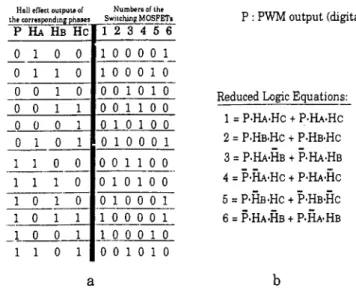
Six MOSFET switches in the switching amplifier provide the voltage and current reversals for rotation. The Hall device feedback and the commutation circuitr}^ determine the switching sequence of the six MOSFETS. Figure 2-6 and Table 2.1 show the MOSFET arrangement
The commutation points in Figure 2-7a center the peak of the back EMF waveform in the commutation zone, and provide equal sharing of the motor phases in the process of producing torque. However, due to the commutation points the variation in the Ky of the motor is approximately 50% for the back EMF waveshape shown. To improve this variation of torque during commutation, called torque ripple, consider the scheme shown in Figure 2-7b. In this case, the motor is commutated twice as often during one revolution by using the negative half of the back EMF waveform as well as the positive half. The torque now falls appro.ximately 13% below the peak. Further improvements can be achieved by modifying the shape of the back EMF waveform so that it is more trapezoidal, so that the back EMF waveform is flat during the period of commutation. The ripple of this type of motor is much less than a motor with a sinusoidal back EMF.
One of the most common forms of brushless DC motor amplifiers is the Cur rent Mode or Current Loop configuration. This type of amplifier uses the PW M technique to control motor current, thereby controlling motor torque output. If
the PW M duty cycle is a function of the difference between the actual and de sired motor current, the loop on motor torque is effectively closed. However, a sensing device to monitor motor current must be introduced. The monitored motor current signal is compared to the desired or commanded current; the erro}· is amplified and compensated, and the result is used to vary the duty cycle of the PW M signal to the power transistors.
Chapter 3
M O D E L L IN G OF T H E
B R U SH LE SS M O T O R A N D
A M P L IF IE R U S IN G SPICE
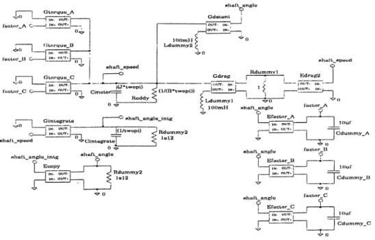
Although SPICE is designed as an electronic circuit simulator, it can also be used to simulate mechanical or electro-mechanical systems. Model of the motor and amplifier will be treated in the sequence.
3.1
Model of the Brushless Motor
The first step in modeling the motor is to develop an electrical equivalent to the mechanical system. The basic equation which describes the mechanical system is:
Tioial =
(IP (3.1)
where
Ttotai is total torque (including friction) applied to the motor shaft from all sources (g · cm)
J is the moment of inertia of the mechanical system {g ■ cm. ■ s^) 6 is the motor shaft angle (radians)
This equation can also be expressed as the following two equations:
Tiotal - 2% J
dt (3.2)
S = — ~
2-K dt (3,3)
where
S is the shaft speed (rev/sec).
Note that the circuit equation for a capacitor is:
- 4
(3.4)Hence, we can implement equation (3.2) by modeling torque as a current and the moment of inertia 27tJ, as a capacitor. This will give the shaft speed as
the voltage across the capacitor. This is convenient because we can model any additional moment of inertia as an additional capacitor in parallel with the first one. Also, we can add various torque and drag forces as parallel current sources. This makes the model easier to use in a system.
We can use equation (3.4) again on equation (3.3) to give the shaft angle as the voltage across a capacitor which has a current equal to the shaft speed applied to it.
To use the model, we apply a current proportional to the shaft torque between nodes SHAFT-SPEED and 0 (1 amp — I g ■ cm) shown in Figure (3-2). The voltage on that node will correspond to the shaft speed (1 volt = 1 rev/sec), and the voltage on SHAFT-ANGLE will be shaft angle (1 volt = 1 radian).
Now we need to model the mechanical losses of the motor. The simplest ones are linear losses: damping and eddy current losses. They are described by the equation:
T,
damping = 27tB - S(3.5)
where
B is the damping and eddy current losses {g ■ cm ■ sec/rad) and is a constant
S is the shaft speed (rev/sec)
We translate into our model units and get:
1{SHAFTSPEED) = 2nB
· V{SHAETSPEED)
(3.6)
This is just the equation for a resistor attached to node SHAFT-SPEED and ground, with a resistance value of
Another mechanical loss is the frictional loss. This loss is a fixed torque which opposes the direction of rotation. To model this loss we use a table to specif}’ the shape of the loss curve and a current source to multiply the loss curve by the loss factor P{g ■ cm)
Another torque is the magnetic detent torque which tends to align the rotor magnetic poles with the stator poles. This torque is periodic, and is described by the equation:
where
T d eten t
=
D ·s'm{Nd
· A - 9 )(3.7)
D is the magnetic detent torque (g ■ cm) and is a constant A is the number of north poles on the rotor and is a constant
Nrf is an integer determined the number of stator slots and the structure of the rotor.
We can translate this directlj' into a current source. Now we need to model the electrical properties of the stator windings. The properties which are required for a first order model are winding inductance, winding resistance, winding ca pacitance, winding mutual inductance, winding back emf, and the torque on the rotor from the winding current. The first four of these are simple electrical prop erties of the winding which are modeled directly by SPICE. For the last two, following [1], we get the following equations for back emf and torque:
Vbn = C k - S - s m { A - 6 - ( N - l ) ^ ) (3.8)
T,n = C f r n - s m { A - e - { N - l ) = p ) (3.9)
where
Vfcn is the back emf voltage for the phase n winding Cb is the back emf voltage constant (volts-sec/rev)
Tdn is the drive torque from the phase n winding Ct is the torque constant (g-cm/amp)
i„ is the current in the phase n winding (amp) S is the shaft speed (rev/sec)
A is the number of north poles on the rotor N is the phase number (1, 2, 3 in our case) P is the number of motor phases
Figure (3-1) shows the electrical part of the motor model drawn using the Schematic Tool of SPICE. Figure (3-2) shows the mechanical part of the motor model drawn using the Schematic Tool of SPICE.
Figure 3-1: Schematic drawing of the electrical jDart of the motor
3.2
Model of the Brushless Amplifier
To model the brushless amplifier, we first need to model the Hall effect device outputs of the motor. Hall effect devices are used to sense the magnetic field of the rotor and produce TTL level outputs. For example, if the backemf voltage waveform of Phase A is positive the sensor output is logic high otherwise low. This can easily be modeled by a voltage controlled voltage source.
In order to model the 6-step commutation strategy we need to design the logic which will implement the desired switching sequence according to the feedback from Hall effect sensors. The PW M input must also be introduced to distinguish between State 1 and State 2, as described in Table2.1. Using logic high to turn on and logic low to turn off the transistors we obtain the following truth table shown in Figure(3-3a)
Hall effect outputs of Numbers of the Switching MOSFETs P Ha Hb H e 1 2 3 4 5 6 0 1 0 0 1 0 0 0 0 1 0 1 1 0 1 0 0 0 1 0 0 0 1 0 0 0 1 0 1 0 0 0 1 1 0 0 1 1 0 0 0 0 0 1 0 1 0 1 0 0 0 1 0 1 0 1 0 0 0 1 1 1 0 0 0 0 1 1 0 0 1 1 1 0 0 1 0 1 0 0 1 0 1 0 0 1 0 0 0 1 1 0 1 1 1 0 0 0 0 1 1 0 0 1 1 0 0 0 1 0 1 1 0 1 0 0 1 0 1 0 P : PWM output (digital)
Reduced Logic Equations:
1 = P.Ha.Hc + P.Ha.Hc 2 = P-Hb-Hc + P-Hb-Hc 3 = P.Ha-Hb + P.Ha.Hb 4 = P‘Ha*Hc + P-Ha-Hc 5 = P-Hb-Hc + P-HB‘Hc 6 = P.Ha.Hb + R Ha-Hb
Figure 3-3: Truth Table and reduced Logic Equations of Switching Amplifier
Taking advantage of the classical method of Karnough maps the truth table can be expressed by the logic equations shown in Figure(3-3b). The implemen tation of the equations in SPICE is made by using the standard TTL AND-OR
gates. To control the current delivered to the motor a PWM model has to be in troduced. This is easily accomplished by using a comparator OP-AM P as shown in Figure(2-5). The spice model is very similar with an 20kHz triangular-wave os cillator connected to the inverting input and the analog feedback signal connected to the noninverting input of the OP-AMP.
3.3
Simulations
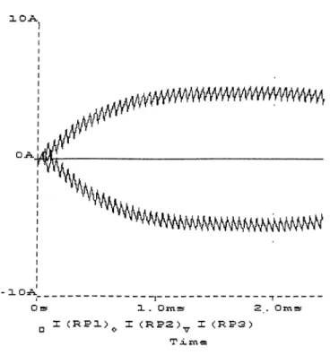
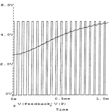
In order to verify the models of the motor and amplifier two sets of simulations are done. First set considers the transient behavior of the system where a step current command of 5 Amps is applied. From the Figure(3-4) and Figure(3-5) it can be seen that the shaft speed of the motor is changing linearly with time, whereas the shaft angle has a parabolic nature. This agrees with our previous discussion. As can be seen from the Figure(3-6) the actual phase currents settle at the commanded current value of 5 Amps. The PWM signal of 20kHz appears as noise and has no effect on the shaft. From the Figure(3-7) it can be seen how the current feedback signal effectively changes the the PWM duty cycle.
As the simulation time is increased the nonlinear behavior of the system can be observed. The shaft speed saturates because of the increased backemf term and the shaft angle changes linearly with time as illustrated in Figure(3-8) and Figure(3-9).
S O Om\7
T i m e
Figure 3-4: Shaft Speed Graph for Short Term Simulations
V ( 3 H j a f '- c _ A n g l = ) T i-mct
lOA
o » 1 . Oiti=f 2 . Oxa»
^ X ( R P l ) ^ I <RP2>^ X <RP3)
T irae
6 . ov
T i-rac
Figure 3-7: PWM and Feedback Signals for Short Term Simulation
£ o v
V __»peesdo
1
. ov
HP T r a e
Chapter 4
D E S IG N OF T H E P O S IT IO N
C O N T R O L L E R
4.1
Simplification of the motor model
In order to design the controller we have to simplify the model described in the previous chapter. Once the brushless motor is properly commutated the normal brush-type motor models can be used for closed loop analysis.
Ra La Ea la
1
E b (fy B-Qj~)
JFigure 4-1: Brush type motor model
As can be seen from the Figure(4-1) the electrical and mechanical equations which describe the behavior of the system are:
Ea = E h R a · la + Ladia
, í ‘ e „ M „ ,
where
Ea : applied voltage (armature voltage) Eb : backemf voltage
Ra : winding resistance La : winding inductance Kt : torque constant
J : total inertia (motor+load) B : friction
Taking Laplace transform of equations (4.1) and (4.2), we obtain:
Ea{s) = Eb{s) + Ia{s) ■ [fía + sLa]
(4.2)
(4.3)
[Js^ + Bs] · ^(s) = Ia{s) ■ Kt (4.4)
In our case the amplifier has a current loop and can be treated as a current source. Hence, the above equations reduce to:
Kt Ojs) ____________ Ia{s) [Js'^ + Bs] (4.5) la r Kt é 1 Js+B 7 s e ■.
Figure 4-2: Simplified motor model Figure(4-2) shows the equation(4.5) in block diagram.
4.2
Simplification of the amplifier model
In order to simplify the current loop, consider the circuit that performs the PWM. Such a circuit is shown in Figure(4-3).
Vin
A A A
aY t t S(t) Comparator with dead bandFigure 4-3: Phase Generating Circuit
The circuit consists of a comparator with a deadband and an input element that sums Vin with a triangular wa.veform S(t). When the combined input is above a threshold, state 1 is chosen. When the combined input is below a negative threshold, state 2 is chosen.
Figure 4-4: Continuous current mode
states are shown in Figure(4-4).
Consider again the H-bridge configuration for one phase in Figure(4-5) The states are defined as follows:
state 1 :
switch 1, switch 4 ON switch 2, switch 3 OFF
state 2 :
switch 2, switch 3 ON switch 1, switch 4 OFF
J +Vb J
© L ^
Vm - I ' ----1 i© SWITCH 4Figure 4-5: H-type PW M amplifier
Accordingly, the output voltage during state 1 is:
Vm = Vs (4,6)
and during state 2 is:
From the Figure(4-3) it can concluded that the times T l and T2 are given by: T - + K ■ Vin 2 (4.8) T - - K - Vm (4.9)
Note that the constant K has a unit of time over voltage. K is given by [3]:
T K =
A F
(4.10)where A F is the peak-to-peak magnitude of S(t). Accordingly, the average value of the output voltage equals to:
Vm, = V s - T l V s - { T - T l )
T T
2 - V s - Tl T
substituting (4.8) we get the following: - l A 2K ■ Fs Vm = ---Vin (4.11) (4.12) current to voltage
Figure 4-6: Block diagram of the simplified amplifier and motor
constant of 4 for the PWM part of the brushless amplifier.
After combining the current feedback device and compensation factor for the current loop we get the complete model of the brushless s5'stem shown in Figure(4- 6).
In the simplified amplifier model the compansator for the current loop is represented by R1 and the current sensor by the feedback gain a.
4.3
Controller Design
The next step in designing a digital control system is to design the controller. Be fore designing the controller, an appropriate structure for the controller must be selected. This will be influenced b}^ the performance requirements of the system and the processing capability of the processor. The controller may be designed in the continuous domain and then converted into discrete form. Alternative!}', the entire design may be carried out in the discrete domain. In our case the design is carried out in continuous domain and then converted to discrete domain.
e
Kp+ Ki +Kd.s Icom PID controller ' r^ , e rr __ l4?_r T.s. A m plifier Motor -> 1e
Figure 4-7: Simplified position control system
The structure of the controller is chosen to be Proportional, Integral and Derivative (PID). The PID controller is by far the most commonly used control algorithm. Although it is of limited complexity it can be used to solve a large number of industrial control problems. The closed loop transfer function of the control system given in Figure(4-6) is as follows:
2 - R l - K ■ K Kt
Icom[s) {L · s -{■ R) ■ T + 2 ■ a ■ Rl ■ K ■ Vs s ■ [J ■ s B)
(4.13)
In order to determine the control gains, further simplification is made on the closed loop transfer function. For our case L=0.54mH, R=0.933n and T=50/r sec, so the first sum term in the denominator can be neglegted when compared to the second. Therefore, for a = l the amplifier gain can be treated as unit.y.
The desired bandwidth of the position control sj^stem is 20Hz, whereas the bandwidth of the amplifier is greater than 2500Hz. The brushless amplifier in current loop mode has therefore a very high bandwidth and can be considered as unity gain. Additionally, friction(B) can be neglected when compared with intertia(J) thus the block diagram shown in Figure(4-7) is the simplified s,ystem which will be considered in the control system design.
It can be seen that the closed loop system is of third order. For design purposes, it is important to sort out the poles that have a dominant effect on the transient response. In design, we can use the dominant poles to control the dynamic performance of the system, whereas the insignificiant poles are used for the purpose of ensuring that the controller transfer function can be realized by physical components.
Figure 4-8: Poles of the Closed Loop System
The characteristic function of the closed loop system is in the form of:
(¿1^ + 2 (u)„5 + wl) · (s + p)
The dominant poles are specified by the w„ (natural frequency) and ( (damp ing ratio) parameters. For w„ = 150 rad/sec and ( = 0.707 we get
Pi - —106 -f 106j
P2 = —106 — 106j
as the complex conjugate dominant poles. From Reference [11] it has been recognized that if the magnitude of the real pole is at least 5 to 10 times tha.t of a pair of complex dominant poles, then the pole may be regarded as insignificant insofar as the transient response is concerned. Selecting the real pole at
рз = -7 0 0
we obtain a third order equation, which is equated to the closed loop char acteristic equation of our system. After some fine tuning the following gains are used:
Kp=9 Kd=0.05 Ki=170
Figure(4-9) shows the closed and open loop system step responses generated using SIMULINK where the plant was the system shown in Figure(4-6). Note that the controller gains (i.e. PID parameters) are found by using the simplified model given in Figure(4-7), while the simulations are performed by using the model given in Figure(4-6). The results are found to have an overshoot of 7.73 % with 9.5 msec rise time and 59 msec 2% settling time.
Figure 4-9: Step Responses of the Open and Closed Loop S3^stem
4.4
Implementation of PID controller on DSP
The algorithm can be implemented in a straightforward wa}' in a DSP with floating point hardware. Implementation using an ordinar)'^ DSP does, however, require special considerations, because all calculations have to be made in integer arithmetic.
4.4.1 Modification and Discretization
The PID algorithm has several drawbacks. Significant modifications of linear and nonlinear behavior are necessary in order to obtain a practically useful algorithm. To obtain equations that can be implemented using computer control it is also necessary to replace continuous time operations like derivation and integration by discrete time operations. The PID algorithm consists of Proportional (P (t)), Integral (I(t)) and Derivative (D (t)) terms which are summed to get the control signal v(t) as:
where
vit) = P{t) + I{t) + D{t)
(4.14)
P(t) = K , ■ e(i) (4.15)
/(«)
= ^ J e(t) (4.16)D(t) = K, - T , · ^ (4.17)
with the error signal as e[t) = r(t) — y{t) and r{t) as reference.
P r o p o r tio n a l T erm
The proportional term P{t) is implemented simpl,y by replacing the continuous time variables with their sampled equivalences. The proportional term then be comes
P{tk) = Kp{r{tk) - y{tk))
where {t^} denotes the sampling instants.
(4.18)
In tegral T erm
To obtain an algorithm that can be implemented on a computer, the integral term I(t) is differentiated
dl{t) _ Kp
; ( i )
dt Ti
Approximating the derivative by a forward difference gives
^(i/r+l)
li'l'k)
Ap . .
----
k----=
1\■
(4.20)
where h is the sampling period. Finallj'^, rearranging terms, we get the following equation to compute the integral term
Htk+i) = I {it) + ^ ■h-e(tk) (4.21)
Derivative Term
A pure derivative should not be implemented, because the controller gain becomes veiy large at high frequencjc This leads to amplification of high frequency noise. The derivative term is therefore approximated in s-domain by
D{s)
= · lU · Ti s · Kp ■ Td (4.22)
E{s) ^ l + s-Td/N
Parameter N is therefore called maximum derivative gain. In analog con trollers N is given a fixed value, from Reference [4] it is typically in the range of 5-20. Notice that the approximation is good for signals whose frequency con tents are significantly below N/T^. Also notice that the approximating transfer function has a maximum gain of N at high frequencies.
Note that e(t)= r(t)-y(t), and r(t) can be considered constant. Hence, for the derivative term, we may replace e(t) by -y(t). It is also advantageous not to let the deriva.tive act on the set point signal r(t). The set point is constant for most of the time and its derivative is therefore zero. A step change in the set point may, however, cause an undesirable jump in the control variable if the derivative acts on the set point. With these modifications 4.22 can be rewritten as
D(s) = - s ■ K , ■ Ti ■ Y{s)
1 + s ■ TilN (4.23)
P ( f ) I - F T
(4.24)
There are several methods to approximate the derivative. Common methods are the forward difference approximation, the backward difference approximation, Tustin’s approximation and ramp equivalence. These approximations all have the same form
D{tk) - a · D{tk--i) - b ■ iy{tk) - y(ik-i)) (4.25)
and are stable onl}' if |a| < 1. The backward difference approximation gives good results for all values of T j. The parameter a goes to zero as T^ goes to zero. Here the backward difference approximation is chosen.
The following is obtained when Equation(4.24) is approximated b}' a backward differerjce:
\
,
D(tk) - D{tk-i)
rp y{h)-y{tk-\)
+ N ---h--- = ' -----h ---Rearranging terms, gives (4.25) with(4.26)
a = Td
Td + N- h (4.27)
b = Kp - Td- N Td + N - h
which is the formula that will be used to compute the derivative term. (4.28)
The PID Algorithm
Summarizing we find that a practical version of the PID algorithm can be de scribed by the following equations:
D[tk) — ad ■ D{tk^i) + hd{y{tk-\) — y{tk)) v{tk) = P(tk) + H^k) "f D(tk)
u(tk) = f{v{tk))
I{tk+i) = I{tk) + bi{r{tk) - y{tk))
The function f describes the nonlinear characteristic of the actuator.
r -> D
1__
I
i-Figure 4-10: Structure of the PID Controller
The parameters aj, bd, b; are related to the primar}' parameters Kp, T;, T,; and N for the PID controller as follows:
ad = Td
Td + N - h (4.29)
bd = KpNTd
Td + N- h (4..30)
bi = Kph/Ti (4.31)
Since the above equations have to be updated only when the controller pa rameters are changed, they can be computed off line. Notice that the algorithm is in parallel form.
4.4.2
Implementation Issues
Implementation of a PID-controller using a DSP using fixed point arithmetic will now be discussed. To perform fixed point calculations it is necessary to know orders of magnitude of all variables. Because of the parallel form, the P, I and D terms can be scaled and computed separatelj'· and then unified.
Selection of Sampling period
There are several rules of thumb for choosing the sampling period for digital controllers. The sampling period should be short enough so that the pole s =
—N/Td, introduced to limit the high frequency gain of the derivative, can be approximated appropriately. This leads to the following rule of thumb (see [5]):
h - N
~tT 0.1 - 0 . 3 (4.32)
Coefficient Scaling
Beca.use of the wide number range of the parameters, some restrictions must be imposed on the magnitude of coefficients. From simulations in MATLAB it follows that b^ is the largest parameter. A limit should therefore be set on the gain Kp, and the high frequency derivative gain N. If Kp and N are limited to 16, we have b^ < KpN=256 and Kp <16. These parameters must therefore be divided by 256 and 16 respectively before they are stored. To restore the magnitude of the signal, the derivative term must be shifted to the left by 8 bits and the proportional term shifted to the left by 4 bits.
The other parameters, a,d and b,· are within the number range and do not need scaling.
Signal Scaling and Saturation Arithmetic
It must be insured that overflow does not occur when computing the states of the controller .With the structure of the PID controller the states are D{tk) and I{t/;+lj· Care must be also taken so that overflow does not occur when the P, I and D terms are added to obtain v.
The proportional term will alwaj^s be within the number range, since the multiplication of a fraction with a fraction gives a fraction. Overflow can occur if Kp is larger than 1 when the magnitude of the signal is restored. It is therefore necessary to use saturation arithmetic when computing the proportional term.
Since the derivative depends only on the process output, it is difficult to use analytic scaling methods effectively. A good engineering approach is therefore to simulate the closed loop sj'stem and store the output of the derivative for a few representative examples. Since b^ can take large values, saturation arithmetic should be used before storing the derivative. A number of simulations were made in order to obtain typical orders of magnitude of the proportional, integral and derivative term. It turns out, that under normal operation conditions, the variables are within the number range. Since we are allowing a gain larger than one, it is very likely that an overflow will occur under some operating condition, for example during start-up. Saturation arithmetic is therefore used on both states and on the control signal v.
Chapter 5
H A R D W A R E D E S IG N
A block diagram of the s^ystem is shown in Figure(5-1). In the following we discuss each major section of the hardware design.
D u a l P o r t M e m o r y I P r o g r a m '
I
M e m o r y \|/I A D C I E n c o d e r P r o c e s s in g Digital Signal *- ProcessorH
T M S 3 2 0 C 2 5 S e ria l P o r t A d r e s s L o g icFigure 5-1: System Block Diagram
5.1
Digital Signal Processor
The DSP chip is the central processing unit for the system. The DSP used is the 40 MHz version of the TMS320C25 by Texas Instruments. A detailed
O u tp u t P o rt F u n ction D efin ition
0 not used not used
1 DAC data A-PAL
2 not used not used
3 not used not used
4 not used not used
5 Transmit Reg. of ACIA H-PAL
6 Control Reg. of ACIA H-PAL
7 Enable Amplifier H-PAL
8-15 not used not used
Table 5.1: Output Port Map
discussion of the architecture and programming of the DSP is given in [2]. The DSP is clocked at exactly 40 MHz and has an instruction cycle time of 100 ns. It has a 16-bit word size with a 32-bit ALU and accumulator. It uses a 16 by 16-bit parallel multiplier with a 32-bit result to perform multiplications in one instruction cycle. It also provides an internal 16-bit timer.
A 40 MHz clock oscillator with a CMOS level output is used to drive the external clock input of the DSP. To cause a reset on power-up, a power monitor chip from Dallas Semiconductor is used. The DS1231 Power Monitor Chip uses a precise temperature-compensated reference circuit which provides an orderly shutdown and an automatic restart of a processor-based system. On power-up, the chip asserts reset in approximately 500 ms, allowing the clock oscillator to stabilize and the DSP to reset.
The DSP has three interrupt inputs which support either level-triggered or edge-triggered interrupts. The DSP has an I/O space of 16 words. These are divided into 16 input and 16 output ports. Input and output port maps are shown in Table(5.1) and Table(5.2)
Input Port Function Definition
0 not used not used
1 Read Encoder A-PAL
2 not used not used
3 not used not used
4 not used not used
5 Receive Reg. of ACIA H-PAL
6 Status Reg. of ACIA H-PAL
7 Status of Amplifier H-PAL
8-15 not used not used
Table 5.2: Input Port Map
5.2
Memory
The DSP has two independent memory spaces, a program space and a data space, each a.ddressing up to 64 K-words of memory, where the word size is 16 bits. The memory hardware provides two external memory units, a 8 K-word EPROM and 1 K-byte of static Dual Port Ram. A block diagram of the memory hardware is shown in Figure(5-2). PS ,1Select I PS — > -l Logic STRB — j R/W— Adress ^ ,_7---16 /fl3 / 1 3 Data 10 __ M/ M/ ...J Dual 8Kx8 8Kx8 Port EPROM EPROM Memory
Hi-Byte Low-Byte lKx8
\/
/8
16
Figure 5-2: Memory Block Diagram
TMS320C25 processor:
• 16-bit address bus (A15-A0)
• 16-bit data bus (D15 - DO)
• PS\DS\IS (program, data, I/O space select)
• R/H^ (read/write) and STRB (strobe)
Throughout this chapter, Q is used to indicate the duration of a quarter phase of the output clock (CLKOU Tl or CLKOUT2). Since speed and max imum throughput is desired, the TMS320C25 is run with no wait states. The TMS320C25 expects data to be valid no later than 2Q-23 ns after STRB goes low. (This takes 27 ns for a TMS320C25 operating at 40 MHz, Q=25ns). The access times of the CY7C26T35 from C3''press Semiconductor EPROMs are 35 ns max imum from address and 20 ns maximum from chip enable. On the TMS320C25, address becomes valid a minimum of Q-12 ns=13 ns before STRB goes low. Therefore, the data appears on the data bus within 27 ns after STRB goes low, as required bj' the TMS320C25.
The Dual-Port RAM interface is the IDT7130SA35P from Integrated Device Technologз^ The IDT7130SA39P is high speed lKx8-bit Dual-Port Static RAM. The RAM has a 35-ns access time from address and a 25-ns access time from chip enable. Note that these access times are fast enough so that a wait-state generator is not required for this interface.
The DSP also has three blocks of on-chip memory (BO, B l, B2) with a total of 544 words. B l and B2 are always mapped into the data space. BO, which is 256 words in length, can be software configured into either data space or program space. BO is mapped into data space upon power-up. The DSP also contains memory mapped registers and reserved locations which are mapped into data space. The memory maps given in Table(5.3) show program and data memory locations.
Type Program Data. Address
OOOOh-0020h-
OOlFh2000h OOOOh- 0006h- 0060h- 0080h- 0200h- 0300h- 0400h-OOOoh OOSFh 007Fh OlFFh 02FFh 03FFh 0800h DescriptionEPROM, Interrupt Vectors EPROM Internal, Registers Internal, Reseiu'ed Internal, Block B2 Internal, Resexu^ed Internal, Block BO Internal, Block B1
External, Dual Port RAM Table 5.3: Memoiy Map: BO as Data Memor}^
The Address Logic is implemented by using Programmable Array Logic (PAL). For this purpose Cypress Semiconductor PAL22V10D-15PC which has a maxi mum pin to pin delay time of 15 ns is used. The PAL22\T0 is a secoixd-generation programmable logic arra}' device. It is implemented with the familiar sum-of- products (AND-OR) logic and a programmable macrocell, which is a new prod uct. The pi'ogrammable macrocell provides the capa.bility of defining the archi tecture of each output individually. Each of the 10 potential outputs may be specified as I'egistered or combinational. Polarity of each output may also be individually selected, allowixig complete flexibility of output configuration. The logic equations are written in VHDL (Very-high-speed-IC Hardwai'e Description Language).
The A-PAL is also responsible for the address decoding of E-PAL (Encoder Processing) and D /A converter which will be described in the following sections.
5.3
Digital to Analog Conversion
The Digital to Analog converter provides the necessary analog interface to the Brushless Power Amplifier. Functional Block Diagram of the DAC section is shown in Figure(5-3).
12
Figure 5-3: DAC Block Diagram
The Digital to Analog interface is implemented using the AD7547 from Analog Devices. The AD7547 is 12-bit current output DAC with level shifters, data reg isters and control logic for eas}· microprocessor interfacing. Two control signals
CS, W R control DAC selection and loading. Data is latched into the DAC regis ters on the rising edge of WR. The device is speed compatible with TMS320C25 and accepts TTL level inputs.
The primary requirement for the current-output DAC is an amplifier with low input bias currents and low input offset voltage. The current to voltage conversion is made around the LF444CN from National Semiconductor. The LF444 is a low power, .JFET input operational amplifier with high gain bandwidth. It has low input bias current of 50pA(max). The DAC is configured in bipolar mode and has the code table shown in Figure(5-4).
B i n a r y N u m b e r in D A C R e g i s t e r M S B L S B A n a l o g O u t p u t 1 111 1 1 1 1 1 11 1 +Vin( 2 0 4 7 \ ^ 2 0 4 8 ’ 1 00 0 0 0 0 0 0 0 0 1 "^'”(T04s) 1 0 0 0 0 0 0 0 0 0 0 0 ov 0 1 1 1 1 1 1 1 1 11 1 0 0 0 0 0 0 0 0 0 0 0 0 /2048^ ■H m a) V in = 10 V
Figure 5-4: Bipolar Code Table
5.4
Encoder Processing
A_
Encoder Output Waveforms Positive Direction
Encoder Output Waveforms Negative Direction
Figure 5-5: Encoder Output Waveforms
The position feedback hardware was designed to decode the three line quadra ture output of a position encoder and maintain position information which the