https://doi.org/10.1007/s10854-019-01379-w
A detailed study on optical properties of InGaN/GaN/Al
2O
3multi
quantum wells
Ahmet Kürşat Bilgili1 · Ömer Akpınar1,2 · Mustafa Kemal Öztürk1,2 · Süleyman Özçelik1,2 · Zekiye Suludere3 · Ekmel Özbay4
Received: 7 March 2019 / Accepted: 19 April 2019 / Published online: 23 April 2019 © Springer Science+Business Media, LLC, part of Springer Nature 2019
Abstract
In this study optical properties of InGaN/GaN/Al2O3 multi-quantum well (MQW) structures are investigated in detail. Three
samples containing InGaN/GaN/Al2O3 MQWs are grown by using metal organic chemical vapor deposition technique.
Sapphire (6H–Al2O3) is used as the substrate. Forbidden energy band gaps (Eg) of these three samples are determined from photoluminescence and absorption spectra. Results gained from these two spectra are compared with each other. It is found that Eg values are between 2 and 3 eV. For determining refraction index, absorption coefficients, extinction coefficients and
thickness of the films a rare method called Swanepoel envelope method is used. It is seen that results gained from this method are consistent with those in literature.
1 Introduction
In recent years, there are many studies for discovering mate-rials to construct high-efficiency optoelectronic devices. As the result of studies done by different researchers, it is noticed that III-group nitride-based materials are convenient for such studies. Nitride-based semiconductors can oper-ate under high pressure and at high temperature. Because of these properties, they are preferred instead of traditional semiconductors [1]. Nitride-based semiconductors such as GaN and InGaN are promising structures for forming solar cells (SCs), light emitting diodes (LEDs) and high electron mobility transistors (HEMTs). It is difficult and expensive to grow GaN on sapphire directly. Because of lattice mismatch and difference in thermal expansion coefficients, there may come out cracks in the layers if GaN is directly grown on sapphire [2]. To prevent this situation a GaN buffer layer
at low temperature is grown over sapphire first. Decreas-ing temperature of this buffer layer is to optimize lattice mismatch. Though this buffer layer is grown over sapphire, for optimizing lattice mismatch, it may still be at 1010–1015
levels [3]. This situation results with high dislocation den-sity. High dislocation density may effect device performance in a negative way. For this reason, they are called threading dislocations (TDs) [4].
Because Egs of InGaN and GaN are different (Eg values
for InN and GaN ranges between 0.7 and 7 eV) [5] when they are grown together a potential step comes out. This structure is called quantum well (QW). Because there are more than one InGaN layers in the structures they are called MQWs [6].
In this study Egs of InGaN and GaN are determined by using PL and absorbance spectra. A material can be excited by using light. When a photon hits an electron of atom of the material that electron is excited to a higher energy level. Because materials want to be stable this excited electron returns back to its previous level naturally. The extra energy is emitted as a different photon. This physical event is called PL. The energy of the emitted photon absolutely equals to the energy gap between two levels [7]. This energy gap can be measured by using PL peaks. Also, Eg of a material can
be measured by using absorbance spectra. If there is absorb-ance it means there is no reflection. Extinction is the sudden decrease of energy of incident photon in the material [8]. Eg values gained from PL and absorbance are compared and
* Ahmet Kürşat Bilgili
1 Physics Department, Gazi University, Teknikokullar,
06500 Ankara, Turkey
2 Photonics Research Center, Gazi University, Teknikokullar,
06500 Ankara, Turkey
3 Biology Department, Gazi University, Teknikokullar,
06500 Ankara, Turkey
4 Physics Department, Bilkent University, Çankaya,
discussed in results and discussion section. For determin-ing optical properties such as refractive index, absorbance coefficient, extinction coefficient and thickness, a method invented by Swanepoel in 1983 is used [9]. For application of this method to InGaN/GaN MQWs, transmission spec-tra is needed. Transmittance is the ratio between intensities of incident and transmitted light from the sample [10]. In Swanepoel method maximum transmission (TM) and
mini-mum transmission (Tm) values are determined and used by
a convenient software. The method used for determining TM and Tm values is called as Swanepoel envelope method.
Results gained from this method are in good accordance with those in literature.
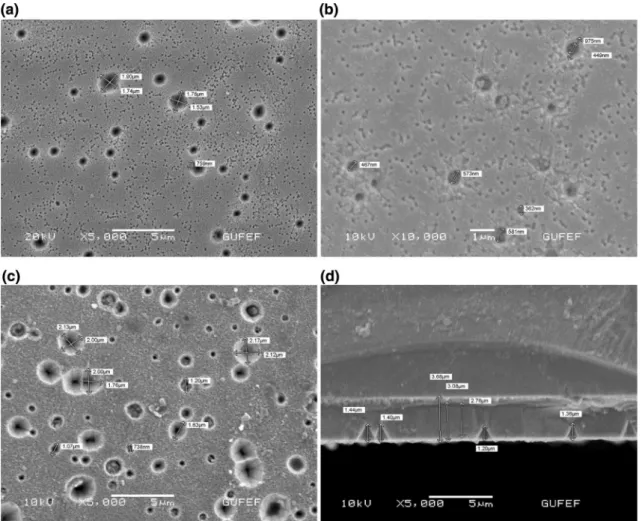
Surface morphology of the samples can be determined by using Scanning Electron Microscope (SEM). SEM has greater resolution and magnification ratio (25 × 103)
accord-ing to optical microscopes. Electrons emitted from electron source are accelerated and they hit the sample surface. Some of these electrons are reflected by elastic collisions and some of them cause secondary electrons by inelastic collisions [11]. These secondary electrons form the image in SEM.
2 Experimental
Trimethylgallium (TMGa), trimethylindium (TMIn) and ammonia are distorted to Ga, In and N, respectively. This distortion is made in Aixtron 200/4 HT-S MOCVD reac-tor. Distortion is separation of Ga, In and N in TMGa and TMIn. GaN (LT-GaN) is grown on Al2O3 substrate under low pressure and at low-temperature condition. InGaN layer is grown on this layer by using TMGa, trimethyla-luminium (TMAl) and ammonia. Transfer of these gasses is maintained by using high-temperature H2 source. Three samples are formed and they are called as sample A (S.A.), sample B (S.B.) and sample C (S.C.), respectively. Sapphire
substrate is cleaned from oxide layer over it by annealing at 1100 °C for 10 min under nitrogen atmosphere. This clean-ing operation is applied before epitaxial growth. LT-GaN layer is grown on substrate to decrease lattice mismatch. All three samples contain LT-GaN buffer layers with different thicknesses (Fig. 1). After growth of LT-GaN buffer layer, five GaN layers are grown on it under 200 mbar constant pressure to decrease dislocations. This operation is applied to all three samples. In S.A. there are LT-GaN layer grown in 2.45 min, five undoped GaN layers (1.9 μm thick in total), 1.9 μm thick n-GaN, 200 nm InGaN, 25 nm graded InGaN, 50 nm p-InGaN and 20 nm thick p-InGaN. In S.C., there are LT-GaN layer grown in 3.30 min, five undoped GaN lay-ers (2.1 μm thick in total), 2.04 μm n-GaN, 20 nm InGaN, 160 nm graded InGaN, 20 nm InGaN, 50 nm p-InGaN and 20 nm thick p-InGaN layers. In S.B. there are similar layers as shown in Fig. 1.
3 Results and discussion
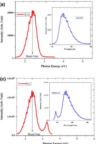
In this study, optical properties of InGaN/GaN/Al2O3 MQWs are characterized by using PL, transmission and absorbance spectra. Jobin-Yvon Fluorolog-550 PL device is used for taking PL data. In this system for excitation 50 mW HeCd (λ = 325 nm) laser source is used. Figure 2 shows PL spectra of three samples. In this figure a, b and c plots show energy dependent PL spectra and inserted plots show wavelength dependency of PL spectra.
It is possible to gain forbidden energy band gaps (Egs) of the samples by using the peak in PL spectra. The peak center in energy versus intensity plot gives directly the Eg value.
Energy values are calculated by the help of wavelengths. To determine energy dependent on wavelength, (E = hc/λ) equation is used. For S.C., in PL spectra there is one more peak on the left of InGaN peak. This peak is estimated to
belong GaN active layer. In literature, Eg of InGaN is in blue
region [12] but here it is found shifted to green region. This situation may be caused by In content. Because of In con-tent, there may be shifts in PL spectra from expected region [13]. In wavelength dependent PL spectra in inserted plots, it is seen that there is a decrease in PL intensity after 600 nm wavelength. This means that there are no other energy levels belong to any component of InGaN. As a result for all three samples, Eg values are found between 2 and 3 eV. Also, there
are many splitting peaks on PL spectra. These maybe caused because of MQW structure of the samples.
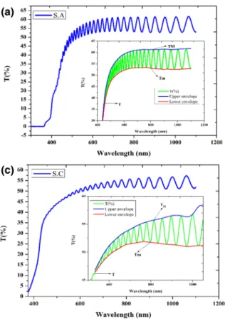
Transmission measurements of InGaN/GaN/Al2O3
MQWs are made. By using optical transmission spectra, thickness of the films, refractive index, extinction coefficient and absorption coefficient can be calculated. In the equations below ns is the refractive index of bottom layer, sapphire. In
Fig. 3, transmission spectra of three samples can be seen. In the inserted plots of Fig. 3 TM and Tm are maximum and
minimum values of transmission interference pattern. They are drawn as upper and lower envelopes as a function of wavelength by using a convenient software [14].
Atomic radius of the elements Ga and N are also effec-tive in transmission spectra. Atomic radius can be cal-culated by using Eq. (3). In this equation r is the atomic radius, r0 is the basic atomic radius and it equals to 1.2
fermi. A is mass number. Results gained from this equa-tion are listed in Table 1.
If TM and Tm are represented with a mathematical model we gain Eq. (1). The equation for refractive index is given in Eq. (2). N in Eq. (2) can be calculated by using Eq. (4). In this equation 1/2 and 2 are calibration coeffi-cients used for nitride based semiconductors.
(1) TM= Ax B− Cx + Dx2 Tm= Ax B+ Cx + Dx2 (2) n= [N + (N2 − n2 s) 1∕2]1∕2 (3) r= r0× A1∕3
Film thickness can be calculated by using adjacent TM
and Tm values in the inserted plots in Fig. 3. The refractive index values n(λ1) and n(λ2) [15] corresponding to these
adjacent TM and Tm values are used in thickness Eq. (5).
t in Eq. (5) is thickness of the film [16].
Variation of refractive index dependent on wavelength is shown in Fig. 4. In S.B. refractive index values show a fluctuated behaviour. The reason for this may be the density of pinholes on the surface or inhomogeneous In content in the structure [17]. Pinholes are described and (4) N= 1 2(1 + n 2 s) + 2ns(TM− Tm) TM× Tm (5) t= 𝜆1× 𝜆2 2[n(𝜆1)𝜆2− n(𝜆2)𝜆1]
shown in Fig. 6 SEM images. For S.A. and S.C. refrac-tive index values and their variation dependent on wave-length are normal and in accordance with literature. For S.A. refractive index is nearly constant at all wavelengths.
Fig. 3 Transmission spectras for InGaN/GaN/Al2O3 MQWs
Table 1 Atomic radius of Ga
and N Element A r (fm)
Ga 31 0.20389
N 7 0.12416
Fig. 4 Variation of refractive index dependent on wavelength for InGaN/GaN/Al2O3 MQWs
This means S.A. has good crystal quality and optimized growth conditions.
For weak and optimum absorption region absorption coefficient α is not equal to zero and x in Eq. (1) is smaller than 1. For this region calculation of refractive index is given in Eq. (2). x in Eq. (1) can be calculated with Eq. (6).
Here EM is given with Eq. (7).
According to Tm, x can be calculated with Eq. (8),
In this equation Em can be calculated with Eq. (9),
In this study, x is calculated by using both methods and they are found in accordance. In Table 2 x values from both methods are shown. One of the x values in Table 2 is calculated by using TM (upper envelope values in Fig. 3)
(6) x= EM− [E2 M− (n 2 − 1)3 (n2 − n4 s)] 1∕2 (n − 1)3(n − n2 s) (7) EM= 8n 2n s TM + (n 2 − 1) (n2− n2s) (8) x= Em− [E2 m− (n 2 − 1)3 (n2 − n4 s)] 1∕2 (n − 1)3 (n − n2 s) (9) Em= 8n 2n s Tm − (n 2 − 1)(n2− n2s)
and the other is calculated by using Tm (lower envelope values in Fig. 3). They are shown on Table 2 to indicate that any of them can be used for calculations because there is very little variation in the values gained from both defi-nitions. EM, Em, N are parameters needed for calculations they have no name.
Absorption coefficient (α) from x value can be gained by using Eq. (10) [18],
and extinction coefficient (k) can be calculated by Eq. (11),
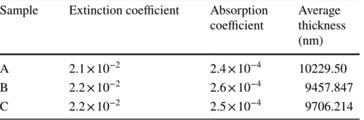
Absorption and extinction coefficients and thicknesses of all three samples are listed in Table 3
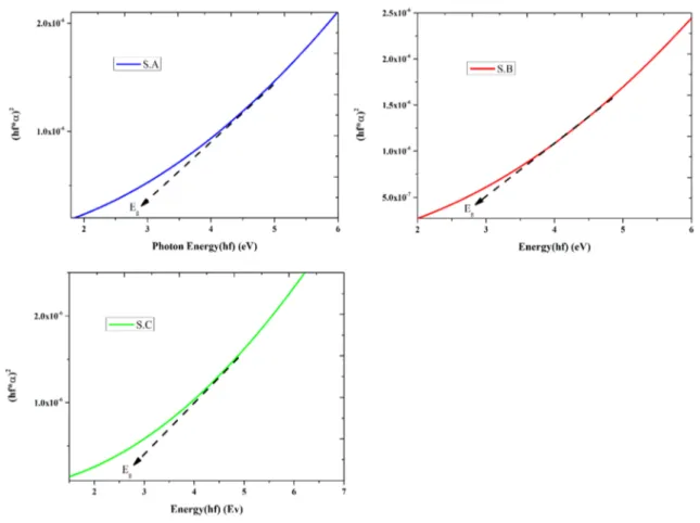
In a semiconductor structure, by measuring the effect of photon energy to absorption coefficient, the forbidden energy band gap of the semiconductor can be gained. For all three samples absorption plots are shown in Fig. 5.
x-axis intercept of high energy region fit in these plots gives forbidden energy gap. As can be seen for all three samples Eg values are between 2 and 3 eV just like the ones
gained from PL spectra. There may be small shifts in meas-ured Eg values from PL and absorbance spectra. The abso-lute values of Eg for these three samples are different from each other but they are all between 2 and 3 eV. For a better approximation this energy range is used.
SEM images for S.A., S.B., and S.C. can be seen in Fig. 6. In these images, pinholes on the surface of the samples can be seen clearly. Because of great lattice mismatch between sapphire and GaN and the difference in thermal expansion coefficients TDs are formed at the interface. These TDs act as micro pipes supporting carrier density in the semicon-ductor structure. At the tip of these micro pipes on the sur-face, there forms holes. Because of their nano, scale they are called as pinholes [19]. Pinholes are not desired in optical and structural terms. For improving electrical properties they may be desired. These structures can also be used as SCs. Pinholes helps increasing carrier density so they are useful in electrical terms.
Dislocation is described as lattice fault. Dislocations may cause even cracking on the surface of crystal. To prevent or minimize dislocations, it is necessary to grow a lattice matched layer on the substrate. To measure dislocation (10) 𝛼= 1 t ln( 1 x) (11) k= 𝛼𝜆 4𝜋
Table 2 X values gained from TM and Tm
Sample X value from TM X value from Tm
A 11.87 11.83
B 11.75 11.70
C 11.82 11.78
Table 3 Optical parameters of the samples A, B, and C Sample Extinction coefficient Absorption
coefficient Average thickness (nm)
A 2.1 × 10⁻² 2.4 × 10⁻⁴ 10229.50
B 2.2 × 10⁻² 2.6 × 10⁻⁴ 9457.847
density there are formulas dependent on XRD data. How-ever, here SEM images are used. Dislocation dots (pinholes) can be counted per cm2 and number of them can be divided
to the area they are found in. Result of this calculation gives dislocation density. In S.A, S.B and S.C dislocation densities are calculated as 108, 2 × 10⁹ and 8 × 109 cm−2, respectively.
These results gained from SEM images are in good accord-ance with one of the previous works done by authors that they calculated dislocation densities from XRD measure-ments [13].
Some lattice spacings in the shape of “V” (Fig. 6d) are determined in SEM images on the cross-section of the sub-strate. Here in local region with statical ion pushing and growing on the sharp side of this inverse “V” deposition of ions with their gravity is seen. This is an interesting and exciting observation.
4 Conclusion
In this paper, optical properties of InGaN/GaN/Al2O3
structures grown by MOCVD are investigated by using PL, transmission, Swanepoel envelope method and absorption spectra. According to PL and absorbance characterization, Eg values of all three samples are found between 2 and 3 eV. By using Swanepoel envelope method thicknesses of the films on sapphire are found around 10,000 nm. This result in accordance with growth conditions. Refractive index values are found around 1.76 and x values needed for absorption and extinction coefficient are found around 11. It is seen that all the results gained in this study are in good accordance with the previous works done by different authors.
Acknowledgements This work was supported by the Presidency Strat-egy and Budget Directorate (Grants Number: 2016K121220).
References
1. S. Nakamura, S. Pearton, G. Fasol, The Blue Laser Diode (Springer, Berlin, 2000). https ://doi.org/10.1007/978-3-662-04156 -7
2. H. Morkoç, Hand Book of Nitride Semiconductors and Devices (Wiley, Berlin, 2008), pp. 1–129. https ://doi.org/10.1002/97835 27628 438
3. S. Nakamura, The roles of structural imperfections in InGaNbased blue light-emitting diodes and laser diodes. Science 281(5379), 956–961 (1998). https ://doi.org/10.1126/scien ce.281.5379.956
4. D.M. Graham, A. Soltani-Vala, P. Dawson, M.J. Godfrey, T.M. Smeeton, J.S. Barnard, M.J. Kappers, C.J. Humphreys, E.J. Thrush, J. Appl. Phys. 97, 103508 (2005). https ://doi. org/10.1063/1.18970 70
5. S.D. Lester, F.A. Ponce, M.G. Crawford, D.A. Steigerwald, High dislocation densities in high-efficiency Gan-based light-emitting diodes. Appl. Phys. Lett. 66(10), 1249–1251 (1995).
https ://doi.org/10.1063/1.11325 2
6. S. Chichibu, T. Azuhata, T. Sota, S. Nakamura, Spontaneous emission of localized excitons in InGaN single and multi-quantum well structures. Appl. Phys. Lett. 69(27), 4188–4190 (1996). https ://doi.org/10.1063/1.11698 1
7. J.R. Taylor, C.D. Zafiratos, M.A. Dubson, Modern Physics for Scientists and Engineers (Colorado University, Boulder, 2004), pp. 101–115
8. X. Liu, M. Atwater, J. Wang, Q. Huo, Extinction coefficient of gold nanoparticles with different sizes and different cap-ping ligands. Colloids Surf. B 58(1), 3–7 (2007). https ://doi. org/10.1016/j.colsu rfb.2006.08.005
9. Y. Jin, B. Song, Z. Jia, Y. Zhang, C. Lin, X. Wang, S. Dai, Improvement of Swanepoel method for deriving the thick-ness and the optical properties of chalcogenide thin films. Opt. Express 25(1), 440–451 (2017)
10. I. Cekic-Naga, F. Egilmez, G. Ergun, Comparison of light trans-mittance in different thicknesses of zirconia under various light curing units. J. Adv. Prosthodont. 4(2), 93–96 (2012). https :// doi.org/10.4047/jap.2012.4.2.93
11. J.I. Goldstein, D.E. Newbury, P. Echlin, D.C. Joy, C. Fiori, E. Lifshin, Scanning Electron Microscopy and X-Ray Micro Analysis (Plenum Press, New York, 1981). https ://doi. org/10.1007/978-1-4615-0215-9
12. S.T. Bayrak, InGaN/GaN multi quantum well light emitting diodes. Doctora thesis Balıkesir University Science Institude, Balıkesir, 7–11 (2011)
13. A.K. Bilgili, Ö. Akpınar, M.K. Öztürk, C. Başköse, S. Özçelik, E. Özbay, Investigation of structural, optical and morphological properties of InGaN/GaN structure. Appl. Phys. A 125(1), 36 (2019). https ://doi.org/10.1007/s0033 9-018-2338-2
14. J. Sánchez-González, A. Díaz-Parralejo, A.L. Ortiz, Determina-tion of optical properties in nanostructured thin films using the Swanepoel method. Appl. Surf. Sci. 252(17), 6013–6017 (2006) 15. J.C. Manifacier, J. Gasiot, J.P. Fillard, A simple method for the
determination of the optical constants n, k and the thickness of a weakly absorbing thin film. J. Phys. E 9, 1002 (1976)
16. D. Poelman, P.F. Smet, Methods for the determination of the opti-cal constants of thin films from single transmission measurements: a critical review. J. Phys. D 36(15), 1850 (2003)
17. M.Y.L. Mandy, B.D. Aleksandra, E. Herbert Li, Refractive index of InGaN/GaN quantum well. J. Appl. Phys. 84, 6312 (1998).
https ://doi.org/10.1063/1.36895 4
18. R. Swanepoel, Determination of the thickness and optical con-stants of amorphous silicon. J. Phys. E 16(12), 1214–1222 (1983).
https ://doi.org/10.1088/0022-3735/16/12/023
19. A.K. Bilgili, T. Güzel, M. Özer, Current-voltage characteristics of Ag/TiO2/n-InP/Au Schottky barrier diodes. J. Appl. Phys. (2018). https ://doi.org/10.1063/1.50646 37
Publisher’s Note Springer Nature remains neutral with regard to jurisdictional claims in published maps and institutional affiliations.