Nanometer-scale patterning and individual current-controlled lithography
using multiple scanning probes
Kathryn Wilder, Hyongsok T. Soh, Abdullah Atalar, and Calvin F. Quate
Citation: Rev. Sci. Instrum. 70, 2822 (1999); doi: 10.1063/1.1149802 View online: http://dx.doi.org/10.1063/1.1149802
View Table of Contents: http://rsi.aip.org/resource/1/RSINAK/v70/i6
Published by the American Institute of Physics.
Additional information on Rev. Sci. Instrum.
Journal Homepage: http://rsi.aip.org
Journal Information: http://rsi.aip.org/about/about_the_journal
Top downloads: http://rsi.aip.org/features/most_downloaded
the tip-sample voltage bias is varied to maintain a fixed emission current during exposure. We have introduced a capacitance compensation scheme to ensure continuous resist exposure of SAL601 polymer resist at scan speeds up to 1 mm/s. We also demonstrate parallel resist exposure with two tips, where the emission current from each tip is individually controlled. Simultaneous patterning with multiple tips may make SPL a viable technology for high resolution lithography. © 1999
American Institute of Physics. @S0034-6748~99!04906-0#
I. INTRODUCTION
Scanning probe lithography ~SPL! may be used to pat-tern nanometer-scale features on a variety of substrates.1–3In fact, scanning probes have been used to manipulate indi-vidual atoms, achieving perhaps the ultimate lithographic resolution.4,5 However, the serial nature of SPL makes this technology much slower than ‘‘mask’’ techniques such as photolithography, x-ray lithography, or extreme ultraviolet
~EUV! lithography. A potential advantage of a direct write
approach is that it does not require expensive and time-consuming mask fabrication. SPL may also have superior alignment capabilities. Nevertheless, in order for SPL to be-come a viable technique for high resolution lithography, the throughput must be dramatically increased. We believe SPL throughput can be increased by attacking the issue on two fronts: ~1! by increasing the writing speed with a single tip and~2! by patterning simultaneously with multiple probes.
We have previously shown that operating in the hybrid atomic force microscope ~AFM!/scanning tunneling micro-scope ~STM! lithography mode has several advantages over other SPL techniques.6 In this mode, both the tip-sample force and the emission current are independently controlled for resist exposure. The tip is held in contact with the resist surface to minimize beam spreading for enhanced patterning resolution. A voltage bias between the probe and the sample generates the field emission of electrons from the sharp probe tip. The voltage is varied to maintain a constant emis-sion current. The current feedback ensures that a constant dose of electrons is delivered to the resist, yielding uniform lithography even when the resist thickness varies as a func-tion of posifunc-tion. This method has since been adopted by
other groups because of the improved performance and reliability.7,8 The lithographic speed is limited primarily by the bandwidth of the feedback loops used to control force and current. In Sec. II we demonstrate increased patterning speed where electrons emitted from the tip are used to ex-pose the resist.
Further increases in patterning throughput require simul-taneous writing with multiple probes. Minne et al. performed parallel oxidation lithography with an array of cantilevers.9 Since the electric-field-enhanced oxidation process is inher-ently slow, it may not be suitable for high throughput pat-terning. In Sec. III we address the challenges encountered when the resist exposure scheme is extended to multiple tips with individual control of the current from each tip.
II. HIGH SPEED PATTERNING WITH A SINGLE TIP A. Control of the tip-sample force
The mechanical response of the actuator that moves the probe up and down limits the scan speed with constant force maintained. Generally, the piezotube scanner is used as the actuator. This large device typically has a resonance below 1 kHz, limiting the scan speed to below 200 mm/s. Manalis
et al. demonstrated that the tip velocity can be increased by
at least an order of magnitude by using a piezoelectric actua-tor integrated onto the cantilever.10 Minne et al. have used such cantilevers for high speed imaging with multiple tips where the tip-sample force was maintained simultaneously and independently by each cantilever.11,12
As a simpler alternative, we have investigated the feasi-bility of performing exposure lithography in the constant-height AFM mode, where the tip is scanned in contact with the sample without controling the tip-sample force. Minne
et al. found that the quality of oxidation lithography was
a!Electronic mail: [email protected]
b!Present address: Bilkent University, Ankara, Turkey 06533.
2822
higher with constant force maintained. The higher forces be-tween the tip and hard silicon sample apparently damaged the tip and degraded patterning fidelity.13 Because the sur-face of an organic resist is soft and pliable, we do not expect small variations in the applied force to damage the tip. How-ever, excessive force between the tip and sample could cause the tip to penetrate~or scratch! the resist.
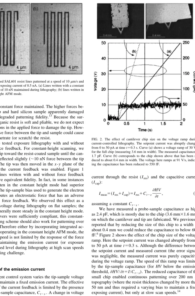
We have tested exposure lithography with and without real-time force feedback. For constant-height scanning, we lowered the tip toward the resist-coated sample until the can-tilever was deflected slightly~;10 nN force between the tip and resist!. The tip was then moved in the x-y plane of the sample and the current feedback was enabled. Figure 1 shows that lines written with and without force feedback appear to have equivalent fidelity. In fact, in some instances patterns written in the constant height mode had superior uniformity. The tip-sample bias used to generate the electron beam contributes an electrostatic force that has an adverse effect on the force feedback. We observed this effect as a variation in voltage during lithography on flat samples; the voltage is generally more steady in the constant height mode. If the cantilevers were sufficiently compliant, this constant-height scanning scheme should also work for patterning over topography. Therefore either by incorporating integrated ac-tuators or by operating in the constant height AFM mode, the lithography speed is not limited by the response of the force feedback. Maintaining the emission current ~or exposure dose! at a fixed level during lithography at high scan speeds is the remaining challenge.
B. Control of the emission current
Our current control system varies the tip-sample voltage bias~HV! to maintain a fixed emission current. The effective bandwidth of the current feedback is limited by the presence of a finite tip-sample capacitance, Ct2s. A change in voltage generates a displacement current proportional to Ct2s. Therefore the total measured current (Imeas)—which the
feedback ties to keep constant—is a sum of the exposing
current through the resist (Ires) and the capacitive current (Icap):
Imeas5~Ires1Icap!5Ires1Ct2s
]HV
]t , ~1!
assuming a constant Ct2s.
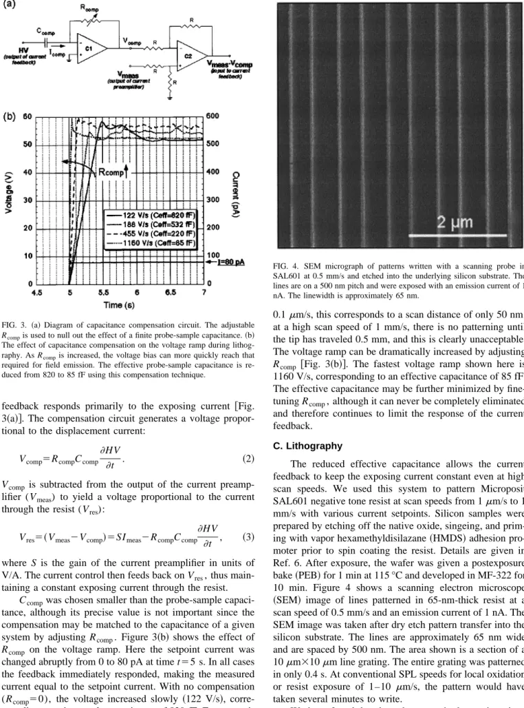
We have measured a probe-sample capacitance as high as 2.4 pF, which is mostly due to the chip~3.6 mm31.6 mm! on which the cantilever and tip are fabricated. We previously reported that by reducing the size of this chip to a width of about 0.4 mm we could reduce the capacitance to below 600 fF.6Figure 2 shows the effect of the chip size of the voltage ramp. Here the setpoint current was changed abruptly from 0 to 50 pA at time t50.3 s. Although the difference between the setpoint current and measured current ~the error signal! was negligible, the measured current was purely capacitive during the voltage ramp. The speed of this ramp was limited by the tip-sample capacitance ~for HV below the emission threshold,]HV/]t5I/Ct2s). The reduced capacitance of the small chip enabled continuous patterning over 200 nm of topography~where the resist thickness changed by more than 50 nm and thus required a varying bias to maintain a fixed exposing current!, but only at slow scan speeds.14
In order to further reduce the influence of the probe-sample capacitance, we build a circuit that compensates for the capacitive component of the current and ensures that the FIG. 1. Developed SAL601 resist lines patterned at a speed of 10mm/s and
with a constant exposing current of 0.5 nA.~a! Lines written with a constant tip-sample force of 10 nN maintained during lithography;~b! lines written in the constant height AFM mode.
FIG. 2. The effect of cantilever chip size on the voltage ramp during current-controlled lithography. The setpoint current was abruptly changed from 0 to 50 pA at time t50.3 s. Curve ~a! shows a voltage ramp of 30 V/s for the full chip~measuring 3.6 mm in width!. The measured capacitance is 1.7 pF. Curve ~b! corresponds to the chip shown above that has been re-duced to about 0.4 mm in width. The voltage here ramps at 91 V/s, indicat-ing the capacitance has been reduced to 550 fF.
2823
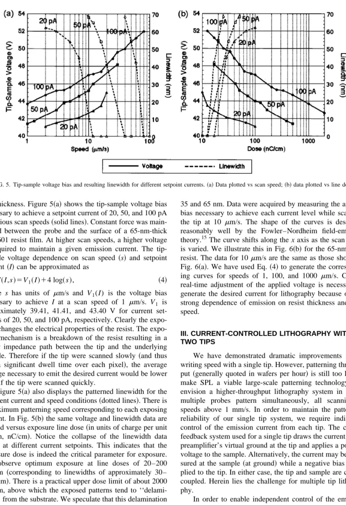
feedback responds primarily to the exposing current @Fig. 3~a!#. The compensation circuit generates a voltage propor-tional to the displacement current:
Vcomp5RcompCcomp]HV
]t . ~2!
Vcomp is subtracted from the output of the current
preamp-lifier (Vmeas) to yield a voltage proportional to the current
through the resist (Vres):
Vres5~Vmeas2Vcomp!5SImeas2RcompCcomp ]HV
]t , ~3!
where S is the gain of the current preamplifier in units of V/A. The current control then feeds back on Vres, thus main-taining a constant exposing current through the resist.
Ccompwas chosen smaller than the probe-sample capaci-tance, although its precise value is not important since the compensation may be matched to the capacitance of a given system by adjusting Rcomp. Figure 3~b! shows the effect of
Rcomp on the voltage ramp. Here the setpoint current was
changed abruptly from 0 to 80 pA at time t55 s. In all cases the feedback immediately responded, making the measured current equal to the setpoint current. With no compensation (Rcomp50), the voltage increased slowly ~122 V/s!,
corre-sponding to a tip-sample capacitance of 820 fF. For approxi-mately 0.5 s there was no exposure. At a slow scan speed of
0.1mm/s, this corresponds to a scan distance of only 50 nm; at a high scan speed of 1 mm/s, there is no patterning until the tip has traveled 0.5 mm, and this is clearly unacceptable. The voltage ramp can be dramatically increased by adjusting
Rcomp @Fig. 3~b!#. The fastest voltage ramp shown here is
1160 V/s, corresponding to an effective capacitance of 85 fF. The effective capacitance may be further minimized by fine-tuning Rcomp, although it can never be completely eliminated
and therefore continues to limit the response of the current feedback.
C. Lithography
The reduced effective capacitance allows the current feedback to keep the exposing current constant even at high scan speeds. We used this system to pattern Microposit SAL601 negative tone resist at scan speeds from 1mm/s to 1 mm/s with various current setpoints. Silicon samples were prepared by etching off the native oxide, singeing, and prim-ing with vapor hexamethyldisilazane~HMDS! adhesion pro-moter prior to spin coating the resist. Details are given in Ref. 6. After exposure, the wafer was given a postexposure bake~PEB! for 1 min at 115 °C and developed in MF-322 for 10 min. Figure 4 shows a scanning electron microscope
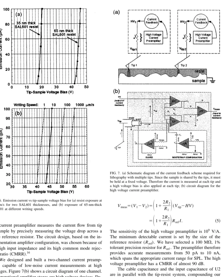
~SEM! image of lines patterned in 65-nm-thick resist at a
scan speed of 0.5 mm/s and an emission current of 1 nA. The SEM image was taken after dry etch pattern transfer into the silicon substrate. The lines are approximately 65 nm wide and are spaced by 500 nm. The area shown is a section of a 10mm310mm line grating. The entire grating was patterned in only 0.4 s. At conventional SPL speeds for local oxidation or resist exposure of 1–10 mm/s, the pattern would have taken several minutes to write.
We have found that the voltage required to emit a given current depends strongly on both the scan speed and the re-FIG. 3. ~a! Diagram of capacitance compensation circuit. The adjustable
Rcompis used to null out the effect of a finite probe-sample capacitance.~b!
The effect of capacitance compensation on the voltage ramp during lithog-raphy. As Rcompis increased, the voltage bias can more quickly reach that
required for field emission. The effective probe-sample capacitance is re-duced from 820 to 85 fF using this compensation technique.
FIG. 4. SEM micrograph of patterns written with a scanning probe in SAL601 at 0.5 mm/s and etched into the underlying silicon substrate. The lines are on a 500 nm pitch and were exposed with an emission current of 1 nA. The linewidth is approximately 65 nm.
sist thickness. Figure 5~a! shows the tip-sample voltage bias necessary to achieve a setpoint current of 20, 50, and 100 pA at various scan speeds~solid lines!. Constant force was main-tained between the probe and the surface of a 65-nm-thick SAL601 resist film. At higher scan speeds, a higher voltage is required to maintain a given emission current. The tip-sample voltage dependence on scan speed ~s! and setpoint current ~I! can be approximated as
V~I,s!5V1~I!14 log~s!, ~4!
where s has units of mm/s and V1(I) is the voltage bias
necessary to achieve I at a scan speed of 1 mm/s. V1 is
approximately 39.41, 41.41, and 43.40 V for current set-points of 20, 50, and 100 pA, respectively. Clearly the sure changes the electrical properties of the resist. The expo-sure mechanism is a breakdown of the resist resulting in a lower impedance path between the tip and the underlying sample. Therefore if the tip were scanned slowly ~and thus had a significant dwell time over each pixel!, the average voltage necessary to emit the desired current would be lower than if the tip were scanned quickly.
Figure 5~a! also displays the patterned linewidth for the different current and speed conditions~dotted lines!. There is a maximum patterning speed corresponding to each exposing current. In Fig. 5~b! the same voltage and linewidth data are plotted versus exposure line dose~in units of charge per unit length, nC/cm!. Notice the collapse of the linewidth data taken at different current setpoints. This indicates that the exposure dose is indeed the critical parameter for exposure. We observe optimum exposure at line doses of 20–200 nC/cm ~corresponding to linewidths of approximately 30– 120 nm!. There is a practical upper dose limit of about 2000 nC/cm, above which the exposed patterns tend to ‘‘delami-nate’’ from the substrate. We speculate that this delamination is due to stress in the resist film resulting from the high dose delivered.
Figure 6~a! shows the current–voltage relationship for electron emission through a SAL601 resist film of thickness
35 and 65 nm. Data were acquired by measuring the applied bias necessary to achieve each current level while scanning the tip at 10 mm/s. The shape of the curves is described reasonably well by the Fowler–Nordheim field-emission theory.15 The curve shifts along the x axis as the scan speed is varied. We illustrate this in Fig. 6~b! for the 65-nm-thick resist. The data for 10 mm/s are the same as those shown in Fig. 6~a!. We have used Eq. ~4! to generate the correspond-ing curves for speeds of 1, 100, and 1000 mm/s. Careful real-time adjustment of the applied voltage is necessary to generate the desired current for lithography because of this strong dependence of emission on resist thickness and scan speed.
III. CURRENT-CONTROLLED LITHOGRAPHY WITH TWO TIPS
We have demonstrated dramatic improvements in the writing speed with a single tip. However, patterning through-put ~generally quoted in wafers per hour! is still too low to make SPL a viable large-scale patterning technology. We envision a higher-throughput lithography system in which multiple probes pattern simultaneously, all scanning at speeds above 1 mm/s. In order to maintain the patterning reliability of our single tip system, we require individual control of the emission current from each tip. The current feedback system used for a single tip draws the current to the preamplifier’s virtual ground at the tip and applies a positive voltage to the sample. Alternatively, the current may be mea-sured at the sample~at ground! while a negative bias is ap-plied to the tip. In either case, the tip and sample are clearly coupled. Herein lies the challenge for multiple tip lithogra-phy.
In order to enable independent control of the emission current from multiple tips, we need a system capable of mea-suring the current at each tip and applying a high voltage to each tip. The sample, shared by all tips, must be held at a fixed voltage. Figure 7~a! depicts this scheme. The high volt-FIG. 5. Tip-sample voltage bias and resulting linewidth for different setpoint currents.~a! Data plotted vs scan speed; ~b! data plotted vs line dose.
2825
age current preamplifier measures the current flow from tip to sample by precisely measuring the voltage drop across a large reference resistor. The circuit design, based on the in-strumentation amplifier configuration, was chosen because of its high input impedance and its high common mode rejec-tion ratio~CMRR!.16
We designed and built a two-channel current preamp-lifier capable of low-noise current measurements at high voltages. Figure 7~b! shows a circuit diagram of one channel. All operational amplifier stages are high voltage devices. De-vice U2 in particular must have an extremely high input impedance and low bias currents since its noninverting input is in parallel with the tip/resist system. We use the Apex Microtechnology high power FET input amplifier PA85 for U1 and U2, and Apex’s PA87A for U3, U4, and U5. The circuit gain is controlled by the ratio R1/R2 and can be
var-ied without affecting the input impedance or the circuit CMRR: Vmeas5~V12V2!5
S
11 2R2 R1D
~Vtip2HV! 5S
112R2 R1D
RrefI. ~5!The sensitivity of the high voltage preamplifier is 109 V/A. The minimum detectable current is set by the size of the reference resistor (Rref). We have selected a 100 MV, 1%
tolerant precision resistor for Rref. The preamplifier therefore
provides accurate measurements from 50 pA to 10 nA, which spans the appropriate current range for SPL. The high voltage preamplifier has a CMRR of almost 90 dB.
The cable capacitance and the input capacitance of U2 are in parallel with the tip-resist system, compounding our previous capacitance problem. We could compensate for these additional capacitances as described in Sec. II. How-ever, since their magnitude far exceeds the original tip-sample capacitance, we cannot expect to reduce the effective capacitance to tolerable levels in this way. Here we show an alternative technique for minimizing the effect of these ca-pacitances. First, we use a triaxial cable between the tip and the preamplifier, where a guard driver is used to raise the cable guard to the tip voltage. Second, we employ a boot-FIG. 6. Emission current vs tip-sample voltage bias for~a! resist exposure at
10 mm/s for two SAL601 thicknesses, and ~b! exposure of 65-nm-thick SAL601 at different writing speeds.
FIG. 7. ~a! Schematic diagram of the current feedback scheme required for lithography with multiple tips. Since the sample is shared by the tips, it must be held at a fixed voltage. Therefore the current is measured at each tip and a high voltage bias is also applied at each tip; ~b! circuit diagram for the high voltage current preamplifier.
strap technique to minimize the 4 pF input capacitance of U2.16The potentiometer is varied to force the current across an external capacitor (Cc) to be equal~and opposite! to the current across the op amp internal input capacitance. Since the input capacitance is somewhat nonlinear, its influence could not be completely eliminated. This capacitance most limits the bandwidth of the current feedback system.
The two-channel current preamplifier was used in con-junction with two identical analog feedback circuits to per-form independent current-controlled lithography with two tips. The integral feedback circuit compares the measured current to the setpoint current and varies HV to minimize the error signal. The current setpoint was enabled with a voltage signal from the computer that controls the movement of the probe in order to synchronize the lithography with the tip motion. The current setpoint can be specified independently for each tip.
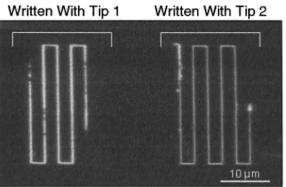
The cantilevers used were 231 arrays of micromachined silicon tips fabricated by Minne and described in Ref. 11. It is important that the two cantilevers are electrically isolated so that the high voltage applied to each tip does not cause significant current flow between the tips. The tips were scanned as a unit along the designated path in the constant height AFM mode. A result of parallel lithography with two tips is shown in Fig. 8, where the pattern on the left was written with tip 1 while the pattern on the right was written simultaneously with tip 2. This current control scheme may be extended to additional tips operating in parallel.
IV. DISCUSSION
We report progress towards higher throughput nano-lithography using scanning probes. A compensation circuit was used to minimize the effect of the tip-sample capaci-tance that limited the effective bandwidth of the current feed-back. This allowed us to demonstrate current-controlled
li-thography of SAL601 resist at speeds up to 1 mm/s. We found that the voltage required to generate the exposing cur-rent depends on the tip scan speed and the resist thickness. The exposure line dose was found to be the critical parameter for lithography.
We also extended the current feedback scheme to two tips, where the exposing current from each tip was indepen-dently controlled. The independent current feedback allows different setpoint currents to be applied to each tip for indi-vidual dose and/or linewidth control. Multiple tip control re-quired a new current preamplifier design with internal ca-pacitance compensation in order to measure currents at high voltages. We demonstrated parallel, current-controlled li-thography of SAL601 resist with two tips.
ACKNOWLEDGMENTS
The authors would like to acknowledge the technical contribution of Stanford Professor Tom Lee with respect to the high voltage preamplifier design. K. W. is pleased to acknowledge the financial support of Advanced Micro De-vices. This work was supported in part by DARPA under Contract. No. MDA972-97-1-0010, by the SRC under Con-tract No. LC-460, and by ONR.
1C. R. K. Marrian, E. A. Dobisz, and R. J. Colton, J. Vac. Sci. Technol. A 8, 3563~1990!.
2E. S. Snow and P. M. Campbell, Appl. Phys. Lett. 64, 1932~1994!. 3J. W. Lyding, T.-C. Shen, J. S. Hubaek, J. R. Tucker, and G. C. Abeln,
Appl. Phys. Lett. 64, 2010~1994!.
4
M. T. Cuberes, R. R. Schlittler, and J. K. Gimzewski, Appl. Phys. Lett. 69, 3016~1996!.
5M. M. Crommie, C. P. Lutz, and D. M. Eigler, Science 262, 218~1993!. 6K. Wilder, H. T. Soh, A. Atalar, and C. F. Quate, J. Vac. Sci. Technol. B
15, 1811~1997!. 7
H. Sugimura and N. Nakagiri, Nanotechnology 8, A15~1997!.
8M. Ishibashi, S. Heike, H. Kajiyama, Y. Wada, and T. Hashizume, Appl.
Phys. Lett. 12, 1581~1998!.
9S. C. Minne, J. D. Adams, G. Yaralioglu, S. R. Manalis, A. Atalar, and C.
F. Quate, Appl. Phys. Lett. 73, 10~1998!.
10
S. R. Manalis, S. C. Minne, A. Atalar, and C. F. Quate, Rev. Sci. Instrum. 67, 3294~1996!.
11S. C. Minne, S. R. Manalis, and C. F. Quate, Appl. Phys. Lett. 67, 3918
~1995!.
12
S. C. Minne, G. Yaralioglu, S. R. Manalis, J. D. Adams, J. Zesch, A. Atalar, and C. F. Quate, Appl. Phys. Lett. 72, 2340~1998!.
13S. C. Minne, P. Flueckiger, H. T. Soh, and C. F. Quate, J. Vac. Sci.
Technol. B 13, 1380~1995!.
14H. T. Soh, K. Wilder, A. Atalar, and C. F. Quate, Proceedings of the 1997
Symposium on VLSI Technology (1997)~Japan Society of Applied Phys-ics, 1997!, p. 129.
15R. H. Fowler and L. Nordheim, Proc. R. Soc. London Ser. A 119, 173
~1928!.
16
A. J. Peyton and V. Walsh, Analog Electronics with Op Amps~Cambridge University Press, New York, 1993!.
FIG. 8. Developed resist lines patterned by two tips simultaneously. The exposing current from each tip was independently controlled.
2827