https://doi.org/10.1007/s10854-019-01233-z
On the possible conduction mechanisms in Rhenium/n‑GaAs Schottky
barrier diodes fabricated by pulsed laser deposition in temperature
range of 60–400 K
Haziret Durmuş1 · Mert Yıldırım2 · Şemsettin Altındal3
Received: 11 January 2019 / Accepted: 26 March 2019 / Published online: 1 April 2019 © Springer Science+Business Media, LLC, part of Springer Nature 2019
Abstarct
This study presents electrical characteristics of n-GaAs based Schottky barrier diodes (SBDs) with Rhenium (Re) rectifier contacts. The electrical characteristics of the Re/n-GaAs SBDs were investigated utilizing the forward bias current–voltage (IF–VF) data collected in temperature range of 60–400 K. The values of ideality factor (n) and zero-bias barrier height (ΦBo)
were found as 9.10 and 0.11 eV for 60 K, and 1.384 and 0.624 eV for 400 K, respectively, on the basis of thermionic-emission theory. The conventional Richardson plot deviated from linearity at low temperatures and the Richardson constant value (A*) was obtained quite lower than the theoretical value for this semiconductor (8.16 A cm−2 K−2). nkT/q–kT/q plot shows
that the field-emission may be dominant mechanism at low temperatures as a result of tunneling via surface states since the studied n-GaAs’s doping concentration is on the order of 1018 cm−3, i.e. at high values so leads to tunneling. On the other
hand, ΦBo–n, ΦBo–q/2kT and (n−1 − 1)–q/2kT plots exhibit linearity but this linearity is observed for two temperature regions
(60–160 K and 180–400 K) due the presence of double Gaussian distribution (GD) of the barrier height. Therefore, the standard deviation value was obtained from the plot of ΦBo–q/2kT and it was used for modifying the conventional Richardson
plot into the modified Richardson plot by which the values of mean barrier height and A* were obtained as 0.386 eV and
15.55 A cm−2 K−2 and 0.878 eV and 8.35 A cm−2 K−2 for the low and high temperature regions, respectively. As a result,
IF–VF–T characteristics of the Re/n-GaAs SBDs were successfully elucidated by double-GD of barrier height.
1 Introduction
It is well known that many semiconductor based electronic and optoelectronic devices; such as transistors, photodiodes and solar cells, are comprised of metal–semiconductor (MS) type Schottky diodes/structures. The quality, reliability and performance of these structures depend on several factors some of which can be listed as the sample temperature, applied bias voltage, the nature of barrier height (BH) at M/S interface, series resistance (Rs), the doping concentration of
donor or acceptors atoms, and so on [1–5]. In addition, a
thin native insulator layer and many surface states (Nss) or
defects can be formed between metal and semiconductor and this strongly influences the performance and conduction mechanisms of MS structures unless particular attention is given during fabrication process to prevent these. Usually, the value of zero-bias BH (ΦBo) for these structures extracted
from the linear part of the semi-logarithmic forward bias I–V plot based on thermionic-emission (TE) theory increases with increasing temperature while the value of ideality factor (n) decreases. A negative temperature coefficient is reported for the forbidden band gap of semiconductor or ideal diodes in the literature [1–4, 6–13], so temperature dependent behavior of BH and n is in consistency with this. In some cases, the conventional Richardson plot may also deviate from the linearity especially at low temperatures and so the obtained value of Richardson constant (A*) from its
intercept point may be much lower than its theoretical value [14–19]. Surface defects and dislocations in semiconduc-tor, roughness of wafer and so its interface with metal, and contaminations at the interface during fabrication process would lead to an effective diode area that is much smaller * Mert Yıldırım
1 Department of Physics, Faculty of Science, Selçuk
University, Konya, Turkey
2 Department of Mechatronics Engineering, Faculty
of Engineering, Düzce University, Düzce, Turkey
3 Department of Physics, Faculty of Science, Gazi University,
than the diodes rectifier contact area, therefore it is expected to find low values for A* and Φ
Bo especially below room
temperatures [6–10, 13–15].
The values of n obtained from the linear part of the Ln(I)–V plot at forward bias region at low and intermedi-ate temperatures are usually much higher than unity due to native or deposited interlayer at M/S interface, the image-force induced BH lowering, inhomogeneous BH distribution at M/S interface, Nss, carrier recombination and generation,
tunneling of charge carriers through BH [19–21]. Recently, the opposite behavior (increase vs decrease) of ΦBo and n
obtained with TE theory during temperature changes was associated with BH’s Gaussian distribution (GD) around a mean value [6–18]. In such case, charge carriers flow through the lower barriers/patches when device operates at low temperatures therefore TE theory reveals high n val-ues. On the other hand, several other conduction mecha-nisms such as field emission (FE), thermionic field emis-sion (TFE), generation-recombination (GR), space-charge limited current, Schottky emission (SE), tunneling and multistep-tunneling (MT) through traps and GD of BH also make contribution to current flow. A specific one of these may become the dominant mechanism for a certain tem-perature and forward bias voltage range [1–3, 22–25]. This brings about the need for conducting measurements in wide temperature range because forward bias I–V characteristics of Schottky type structures at room temperature or narrow temperature range would not provide enough on the possible conduction mechanisms, temperature dependence of elec-trical parameters and the form of barrier at M/S interface. This can be avoided through performing the measurements in wide range of temperature and bias voltage. Thus reliable information on current transport mechanisms or conduction mechanisms, nature of BH at M/S interface and other device parameters can be obtained [16–24, 26–29].
GaAs is a semiconductor which has large and direct band gap, high saturation velocity and high carrier mobility [10,
21, 30]. These features make GaAs quite suitable for fab-rication of MS type Schottky barrier diodes (SBDs) hence GaAs is preferred for high power devices operating at high frequencies. Rhenium (Re) is a shiny metal which is highly corrosion resistant. This material belongs to the class of refractory metals. For the conditions that the samples are exposed to radiation and temperature fluctuations such as metal–semiconductor based electronic devices on satel-lites, durability and resilience of materials become impor-tant. Therefore, high melting point and thermal stability of Re make it quite interesting for its usage as metal contact. Several methods can be utilized for deposition of Re such as chemical vapor deposition [31], sputtering [32] and pulsed laser deposition. There are several studies in which Re was utilized as rectifier [32] or ohmic [33] contact material as well as interlayer material [31]. However, there is only a
scarce number of studies in which Re is used as rectifier contact. To the best of our knowledge, Re/n-GaAs Schottky barrier diodes (SBDs) were not reported previously. There-fore, this study focuses on electrical characteristics of Re/n-GaAs SBDs. For this purpose, forward bias I-V character-istics were investigated between 60 and 400 K for a better interpretation of the possible conduction mechanisms in the SBDs. Experimental results show that temperature depend-ence of ΦBo is opposite to that of n, the former increases
whereas the latter decreases with temperature. Also, devia-tion from linearity was observed for the convendevia-tional Rich-ardson plot especially at low temperatures and so it revealed quite low value for A* compared to its theoretical value. Such
behavior of electrical parameters of Re/n-GaAs SBDs was successfully explained with the existence of GD of BHs at Re/n-GaAs interface.
2 Experimental
Re/n-GaAs SBDs were fabricated using double side pol-ished (DSP) n-type single crystal n-GaAs wafer with (100) surface orientation, having 625 µm thickness. The car-rier concentration was provided between 2.23 × 10¹⁸ and
3.10 × 1018 cm−3 by the supplier. The GaAs wafer was first
degreased in an organic solvent mixture of methyl alcohol, acetone and trichloroethylene for about 5–7 min. Later, it was etched in a sequence of H2SO4 and H2O2, 20% HF, a
solution of 6HNO3:1HF:35H2O, 20% HF. After each step
of the cleaning procedure, the wafer was quenched in de-ionized water with resistivity of 18 MΩ cm. Then, highly pure (99.999%) Au was thermally evaporated on n-GaAs in high vacuum system (10−6 Torr) so that Au ohmic contact
with ~ 200 nm thickness was formed. Then, the sample was annealed at 450 °C for 5 min to ensure low resistivity for the contact [34].
Rectifying contacts were deposited on n-GaAs at room temperature under high vacuum. Before starting material deposition, vacuum level was first dropped down to a base level of 7.5 × 10⁻⁸ Torr using a DUO 20M Rotary Vane
Pump connected to a HiPace 700 turbo molecular pump, both of which were supplied by Pfeiffer Vacuum. When deposition was started, the chamber pressure was about 7.5 × 10⁻⁷ Torr. Rhenium (Re) target material with 99.99%
purity supplied by Goodfellow was utilized to form Re rec-tifying contacts using Pulsed Laser Deposition (PLD) tech-nique. The target’s distance to the substrate was arranged as 40 mm during the deposition. The target and wafer were both rotated at a speed of 10–15 rev/min to increase the homogeneity of the contacts. During the deposition, a metal shadow mask was utilized to obtain rectifying contacts with diameter or 1.5 mm diameter. Finally, Re rectifying contacts with 200–250 nm thickness were formed after a deposition
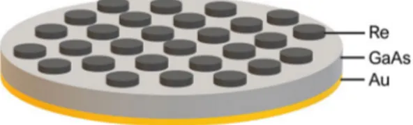
duration of about 2 h. 3D Schematic representation of the fabricated Re/n-GaAs SBDs is given in Fig. 1. Once the fabrication is completed, the current–voltage (I–V) meas-urements in the voltage range of (− 1 V)–(+ 2 V) with 5 mV steps were conducted using a Keithley 2410 source meter in the temperature range of 60–400 K.
3 Results and discussion
The typical forward and reverse bias I–V data of the Re/n-GaAs SBD were plotted in the wide temperature (60–400 K) and voltage [(− 1 V)–(+ 2 V)] ranges and given in Fig. 2. As shown in Fig. 2, each forward bias I–V plot has a fine linear region with varying slopes in the intermediate bias region. The forward bias current keeps increasing with increasing forward bias voltage however deviation from the linearity occurs because of increasing voltage drop due to Rs towards
higher biases. The reverse bias current as well keeps increas-ing. Such non-saturating reverse bias I–V characteristics is believed to stem from the contribution of recombination current and the contribution due to lowered BH induced by image-force [26, 27]. Although leakage current is increased with bias, it is clear in Fig. 2 that reverse bias I–V saturation ability of the device at 400 K is better than that at 60 K. Such kind of better saturation performance at high temperatures is because space-charge region expands as the temperature is increased, thus saturation of leakage current occurs at lower reverse bias voltage.
According to TE theory, when a SBD was applied with a forward bias voltage larger than 3kT/q, the current passing through the BH is given by [1–4];
where Io, q, V, k and T are well-known diode parameters
given elsewhere [1–3]. The values of Io are obtained through
y-intercept of the linear part of Ln(I)–V plot whereas n can be extracted using slope of this linear part in the following relations [1–3];
Io is also given by the following relation [1–3];
where A is the area of rectifier contact and A* is the effective
Richardson constant, which is 8.16 A cm−2 K−2 for n-GaAs.
Thus Io value obtained on the basis TE theory can be used to calculate ΦBo value by converting Eq. (3) into the following
form [1–4, 6–15];
These electrical parameters of the Re/n-GaAs SBD were obtained for each temperature level and tabulated in Table 1. It is clear that these parameters are strong func-tions of temperature. As seen in the table, the values of Io, n,
ΦBo change from 3.60 × 10⁻⁷ A, 9.10, 0.109 eV (at 60 K) to
3.20 × 10⁻⁴ A, 1.384, and 0.624 eV (at 400 K), respectively.
Figure 3 shows opposite response of ΦBo and n to
increas-ing temperature. Observed behavior in Fig. 3 and particu-larly high values of n especially at low temperatures can be partly explained by the existence of a native interlayer, spatial distribution of Nss at M/S interface, barrier lowering
due to image-force, inhomogeneous barrier at M/S inter-face and TE theory’s becoming less dominant [2–4, 19–22,
35]. In addition, Saad and Kassis [36] attributes high values of n in solar cell to current’s being dominated by interface (1) I= Io [ exp( qV nkT ) − 1 ] (2) n= q kT ( dV d(ln I) ) (3) Io= AA∗T2 exp ( −q𝛷Bo kT ) (4) 𝛷Bo= kT q ln [ AA∗T2 Io ]
Fig. 1 3D schematic representation of the Re/n-GaAs SBDs
Fig. 2 I–V characteristics of the Re/n-GaAs SBD in the temperature
recombination. However, we believe the main reason of high values of n at low temperatures is the barrier inhomogeneity at M/S interface [9–22].
Table 1 also shows temperature dependent series resist-ance, Rs, of Re/n-GaAs SBD. Rs is an important device
parameter which considerably affects the forward bias I–V characteristics of Schotky type MS and MIS struc-tures especially at sufficiently high forward bias voltages since the value of voltage drop, IRs, becomes larger and
less amount of bias voltage is felt by the structure. The value of Rs of the Re/n-GaAs SBD was also calculated
at 2 V using Ohm’s law for each temperature level. Rs is
decreased with increasing temperature because (1) forbid-den bandgap of semiconductor is shrunk and (2) carriers’ thermal energy is increased. More importantly, low values of Rs were obtained for Re/n-GaAs. This result is believed
to be an advantage of Re contacts’ being grown with Laser Deposition (PLD) technique. This technique is promising for future of MS structures and encourages researchers to utilize it because of its advantage of being more functional and controllable. Moreover, this technique makes it pos-sible to deposit Re contacts considering very high melting point of Re. Therefore, recently, high-resistance interfaces barriers, high corrosion resistance and its potential for thermoelectric applications make Re-semiconductor (MS) type SBDs gain more attention of researchers [37–40]. It is well known that some metallic materials for the formation of rectifier contacts on the semiconductor have high melt-ing temperature. In this study, rectifier contacts (Re) were performed at 3180 °C/5627 °C, on n-GaAs semiconduc-tor. Such temperature value is sufficiently high regarding temperature-resistant contacts needed by high temperature applications. Experimental results show that the PLD nique appears to be the most appropriate production tech-nique for Re-semiconductor (MS) type SBDs. Therefore, the obtained value of Rs by Ohm’s was found as 15.62 Ω
even at 60 K which is very suitable for MS type structures. In addition the value of n is closer to unity (ideal case) above room temperatures.
Equation (3) can be further useful through modification as below;
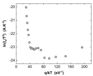
According to this equation, plot of ln(Io/T2) vs q/kT (the
Richardson plot) could be used for the evaluation of ΦBo
or activation energy (Ea) as a second way because slope of
this plot simply reveals ΦBo whereas A* can be extracted
from the y-intercept value. Therefore, Richardson plot of the Re/n-GaAs SBD was given in Fig. 4. However, this plot is not employable because it considerably deviates from the linearity at low temperatures (below room tem-perature in our case). Moreover, the value of Richard-son constant (A*) is obtained much lower than its
theo-retical value (8.16 A cm−2 K−2) although only the linear
section of the Richardson plot is utilized. It is believed that the temperature dependent behavior of ΦBo and n
depicted in Fig. 3 leads to non-linearity in the Richard-son plot (Fig. 4) and very low value of A*. The
behav-ior of ΦBo and n in Fig. 3 and that of Richardson plot in
Fig. 4 point out an anomalous behavior. These show that (5) ln( I0 T2 ) = ln (AA∗) − q kT𝛷Bo
Table 1 The experimental values of Io, n, ΦBo, nT and Rs obtained
using the forward bias I–V data of the Re/n-GaAs SBD in the tem-perature range of 60–400 K
T (K) Io (A) n ΦBo (eV) nT (K) Rs (at 2 V) (Ω)
60 3.6 × 10⁻⁷ 9.100 0.109 546 15.61 80 3.3 × 10⁻⁷ 6.605 0.150 528 15.52 100 4.9 × 10⁻⁷ 5.263 0.188 526 15.40 120 6.3 × 10⁻⁷ 4.220 0.227 506 15.23 140 9.0 × 10⁻⁷ 3.623 0.264 507 15.00 160 2.1 × 10⁻⁶ 3.300 0.294 528 14.85 180 3.1 × 10⁻⁶ 3.050 0.328 549 14.60 200 3.7 × 10⁻⁶ 2.730 0.365 546 14.36 220 4.1 × 10⁻⁶ 2.520 0.403 554 14.12 240 5.3 × 10⁻⁶ 2.346 0.438 563 13.91 260 6.2 × 10⁻⁶ 2.181 0.475 566 13.64 280 7.9 × 10⁻⁶ 1.975 0.509 552 13.40 300 1.3 × 10⁻⁵ 1.787 0.536 536 13.13 320 2.6 × 10⁻⁵ 1.646 0.556 526 12.86 340 4.3 × 10⁻⁵ 1.540 0.580 523 12.62 360 8.1 × 10⁻⁵ 1.482 0.598 533 12.33 380 1.5 × 10⁻⁴ 1.446 0.615 549 12.06 400 3.2 × 10⁻⁴ 1.384 0.624 553 11.82
Fig. 3 The variation of ΦBo and n with temperature for the
the current-transport/conduction mechanism at low and intermediate temperatures is considerably different from that at high temperatures thus other mechanisms such as TFE, FE, multistep tunneling via traps, and Gaussian dis-tribution of BH at M/S interface may be dominant rather than TE [7–17]. Therefore, recently, many researchers have focused on the temperature and voltage dependence of BH, n, and A* through experimental data taken in wide
range of temperature and voltage in order to reach detailed information on the possible conduction mechanisms and the form of BH [18–30].
Observed behavior for ΦBo and n with temperature, low
value for A* and non-linearity of the conventional
Richard-son plot were recently associated with inhomogeneous bar-rier height. It is believed that the barbar-rier has potential fluc-tuations and is a combination of lower and higher patches therefore carriers preferably pass through the barrier sec-tions that have lower potential [19–30]. Therefore, even at low temperatures, carriers can pass over the barrier through its lower patches and in this case current conduction is domi-nated by these carriers’ contribution thus large values of n is obtained when the structure operates at low temperatures. As the temperature is increased, the number of carriers which have enough energy for passing through higher patches of barrier increases as a result current contribution of lower patches of barrier becomes negligible and the value of n approaches to unity.
Considering the discussions above, current conduction is not solely governed by TE. For non-uniform highly doped semiconductors, various current-conduction mechanisms may make contribution to current conduction. Although TE would still be dominant at high temperatures, mechanisms such as TFE, FE, Schottky emission, space-charge limited current, multistep-tunneling via traps, and Gaussian distri-bution of BH become dominant below room temperatures
rather than TE theory [7–17, 35, 41–45]. For example, TFE and FE becomes dominant at low temperatures for the structures fabricated with high doping concentration of donor or accepter atoms. It needs to be noted that concen-tration of donor atoms for n-GaAs of this study is given as 2.23 × 10¹⁸–3.10 × 1018 cm−3 by the manufacturer. Arslan
et al. [20], Padovani et al. [23], Crowell et al. [42], Ravi-mendan et al. [43], Çınar et al. [44], Al-Dharob et al. [45] and Taşçığlu et al. [26, 46] showed that both the TFE and FE theories (Quantum mechanical tunneling) will be domi-nant for moderate or highly doped semiconductor devices at low temperatures. Therefore, FE and TFE mechanisms need to be taken into account when the device operates below room temperatures. On the other hand, the requirement of these two conduction mechanisms depends on the relation between the tunneling current parameter Eoo and kT/q. When
FE or TFE is considered, current–voltage relation is given by [23, 41, 42];
Here Eo is a parameter whose relationship with tunneling
parameter, Eoo, is given by;
where ntun is the ideality factor in the case of tunneling. As
mentioned earlier, tunneling depends on the doping concen-tration. Its relation to doping concentration is given by the following equation;
Here h is Planck constant, me* is effective mass of
elec-tron, and ɛs is the permittivity semiconductor and equals to
9.7ɛo for GaAs where ɛo (= 8.85 × 10⁻¹² F/m) is the
permit-tivity of vacuum.
Figure 5 shows the plot of nkT/q–kT/q. This plot provides information on current conduction mechanisms. It is seen that linear fit of nkT/q is almost temperature independent. Such behavior of nkT/q is consistent with the nT values in Table 1. In this case, Eo becomes equal to Eoo whose
theo-retical value was obtained as 45.40 meV using Eq. (6c). However, as seen in Fig. 5, it is clear that the experimental value is considerably higher than the theoretical value of Eoo
(= 45.40 meV). These results show that TFE and FE, both, can be possibly dominant current conduction mechanisms rather than TE theory. Considering that the value of Eoo is
considerably higher than the thermal energy (kT/q) particu-larly in the low temperature region, it can be said that FE is
(6a) I= Itun [ exp ( q(V − IRs ) Eo ) − 1 ] (6b) ntun= Eoo kT coth ( Eoo kT ) = Eo kT (6c) Eoo= h 4𝜋 ( ND m∗ e𝜀s )1∕2
Fig. 4 The Richardson plot of the Re/n-GaAs SBD in the temperature range of 60–400 K
the dominant current mechanism in this region. Nevertheless TFE/FE’s becoming dominant and the existence of native interlayer and surface states at M/S interface alone are not sufficient to explain lower values of ΦBo and higher values of
n at low temperatures. Hence, observed non-ideal forward-bias I–V characteristics of the Re/n-GaAs SBD was further explored on the basis of a TE mechanism with a Gaussian distribution (GD) of barrier height [9–22].
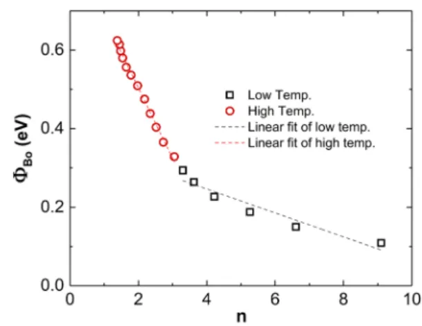
In the literature, an increment in ΦBo and a decrement in n
with increasing temperature is observed for various Schottky devices and such behavior of device parameters was success-fully interpreted through a modified version of TE theory which assumes there exists single or double Gaussian distri-bution (SGD or DGD) for barrier potential [12–30, 45, 46]. Tung [9] and Mönch [14] introduced an approach which con-siders a linear correlation between ΦBo and n to explore an
evidence on GD of BH. Recently, several researchers showed that the plot of ΦBo–n has more than one linear region [17,
21, 22, 28, 30, 46]. Therefore, ΦBo–n plot was drawn for
further investigation on GD and given in Fig. 6. This plot reveals two linear regions suggesting the distribution is in the form of DGD. As proposed by Werner and Güttler [15], in the case of barrier inhomogeneity, the calculated n and
ΦBo values from Eqs. (1) and (3), respectively, are indeed their apparent values which depend on temperature and volt-age. In this case, Eqs. (1) and (3), can be rewritten as [15];
(7a) I= AA∗T2exp ( −q𝛷ap kT )[ exp ( qV napkT ) − 1 ] (7b) I0= AA∗T2 exp ( −q𝛷ap kT )
Thus, GD of the BHs with a mean BH ( 𝛷Bo ) and standard
deviation (σs) based on TE theory is expressed with
follow-ing relations;
In Eq. (8b), ρ2 and ρ3 are voltage coefficients which
quan-tify deformation of BH distribution. Hence, Φap and nap
val-ues were plotted against q/2kT and given in Figs. 7 and 8, respectively, to acquire more information on GD of BH.
As it is clearly seen in Fig. 6, ΦBo–n plot has two
dis-tinct linear regions which are inversely proportional to n in the whole temperature range. Thus, the extrapolation of Φap–n plot (Fig. 6) to n = 1 (for ideal case), the value
(8a) 𝛷ap= 𝛷Bo− q 2kT𝜎 2 s (8b) ( n−1ap − 1 ) = 𝜌2− q 2kT𝜌3
Fig. 5 nkT/q–q/kT plot of the Re/n-GaAs SBD in the temperature
range of 60–400 K
Fig. 6 ΦBo–n plot of the Re/n-GaAs SBD in the temperature range of
60–400 K
Fig. 7 ΦBo–q/2kT plot of the Re/n-GaAs SBD in the in the
of 𝛷B0 was found as 0.356 eV for low temperature region
(60–160 K) and 1.13 eV for high temperature region (180–400 K). Moreover, it is seen that Figs. 7 and 8 also have two linear parts with different slopes. This supports Fig. 6 and strengthens the idea that barrier potential dis-tribution is in the form of DGD. Furthermore, the values of 𝛷B0 and σs were extracted as 0.382 eV and 0.0055 V
for low temperature region, and 0.876 eV and 0.132 V for high temperature region, respectively, through the intercept and slope of Φap–q/2kT plot (Fig. 7)
accord-ing to Eq. (8a). Similarly, the values of ρ2 and ρ3 were extracted as − 0.601 V and − 0.0032 V for low temperature region, and 0.0317 V and − 0.0235 V for high temperature region, respectively, through the intercept and slope of (n−1 − 1)–q/2kT plot (Fig. 8), according to Eq. (8b).
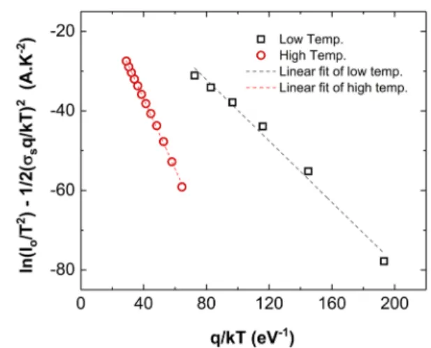
Similar to the extraction of the equation of the conven-tional Richardson plot, Eqs. (7b) and (8a) can be combined together as the following;
This equations shows the importance of 𝛷Bo and σs
because these parameters need to be used while modify-ing the conventional Richardson plot. Now, Eq. (9) can be used to draw a plot of [ln(Io/T2) − ½(qσs/kT)2]–q/kT (i.e.
the modified Richardson plot). Thus, the modified Rich-ardson plot was drawn and given in Fig. 9. The values of A*
and 𝛷Bo were extracted from the intercept and slope of the
modified Richardson plot (Fig. 9) as 15.55 A cm−2 K−2 and
0.36 eV for low temperature region and 8.35 A cm−2 K−2
and 0.878 eV for high temperature region, respectively. It is clear that the effective value of A* obtained from the
modified Richardson plot (Fig. 9) is very close to the theo-retical value of A* for n-GaAs for high temperature region.
(9) ln( I0 T2 ) − 1 2 (q𝜎 s kT )2 = ln (AA∗) − q kT𝛷B0
Moreover, the values of 𝛷Bo are in very good agreement
with those shown in Figs. 6 and 7.
4 Conclusion
In this study, the forward bias IF–VF characteristics of the
Re/n-GaAs SBD were investigated in wide temperature range (60–400 K). I–V characteristics were utilized to obtain in-depth information regarding possible conduction mechanisms, the nature of BH at M/S interface, the origin of high n values at low temperatures and positive temperature coefficient of ΦBo, and the origin of very low value of A*
compared to its theoretical value. When TE theory is con-sidered, ΦBo and n changed from 9.100 and 0.109 eV (60 K)
to 1.384 and 0.624 eV (400 K), respectively. Such behavior of ΦBo and n with temperature is the reason for non-linearity
in the Richardson plot and very low experimental value of
A*. nkT/q–kT/q plot show that the TFE and FE conduction
mechanisms may be dominant at low temperatures because of tunneling via surface states since n-GaAs has high level of doping concentration (ND = 2.23–3.10 × 1018 cm−3). On
the other hand, high values of n at low temperatures can-not be explained by these theories or by the possibility of a native insulator layer and surface states. Therefore, this non-ideal behavior of I–V characteristics in the Re/n-GaAs SBD was associated with a modified version of TE assum-ing a Gaussian distribution (GD) for the barrier potential. Plots of nkT/q–kT/q, ΦBo–n, ΦBo–q/2kT and (n−1 − 1)–q/2kT
revealed two distinct linear regions for the two temperature regions; i.e. low and high temperature results with tem-perature range of 60–160 K and 180–400 K, respectively. This suggested the distribution is of the form double GD. When the Richardson plot was modified, BH and A* were
Fig. 8 (n−1 − 1) versus q/2kT plot of the Re/n-GaAs SBD in the
found as 0.386 eV and 15.55 A cm−2 K−2 for low
tempera-ture region and 0.878 eV and 8.35 A cm−2 K−2 for high
temperature region, respectively. It is clear that this value of A* (= 8.35 A cm−2 K−2) for high temperature region is
quite close to the theoretical value of 8.16 A cm−2 K−2 for
n-GaAs. As a result, it is shown that IF-VF–T characteristics
of the Re/n-GaAs SBDs can be successfully explained by TE theory with the double-GD of BH.
References
1. S.M. Sze, Physics of Semiconductor Devices (Wiley, New York, 1981)
2. B.L. Sharma, Metal-Semiconductor Schottky Barrier Junctions
and Their Applications (Plenum Press, New York and London,
1984)
3. E.H. Rhoderick, Metal-Semiconductor Contacts (Clarendon Press, Oxford, 1978)
4. H.C. Card, E.H. Rhoderick, Studies of tunnel MOS diodes I. Inter-face effects in silicon Schottky diodes. J. Phys. D Appl. Phys. 4, 1589–1601 (1971)
5. E.H. Nicollian, J.R. Brews, MOS (Metal Oxide Semiconductor)
Physics and Technology (Wiley, New York, 1982), pp. 117–129
6. H.H. Güttler, J.H. Werner, Influence of barrier inhomogeneities on noise at Schottky contacts. Appl. Phys. Lett. 56, 1113–1115 (1990)
7. R.T. Tung, J.P. Sullivan, F. Schrey, On the inhomogeneity of Schottky barriers. Mater. Sci. Eng., B 14, 266–280 (1992) 8. R.F. Schmitsdorf, T.U. Kampen, W. Mönch, Correlation between
barrier height and interface structure of Ag/Si (111) Schottky diodes. Surf. Sci. 324, 249–256 (1995)
9. R.T. Tung, Recent advances in Schottky barrier concepts. Mater. Sci. Eng., R 35, 1–138 (2001)
10. M.K. Hudait, K.P. Venkateswarlu, S.B. Krupanidhi, Electrical transport characteristics of Au/n-GaAs Schottky diodes on n-Ge at low temperatures. Solid State Electron. 45, 133–141 (2001) 11. R.T. Tung, Electron transport at metal-semiconductor interfaces:
general theory. Phys. Rev. B 45, 13509 (1992)
12. J.P. Sullivan, R.T. Tung, M.R. Pinto, W.R. Graham, Electron transport of inhomogeneous Schottky barriers: a numerical study. J. Appl. Phys. 70, 7403–7424 (1991)
13. Y.P. Song, R.L. Van Meirhaeghe, W.H. Laflere, F. Cardon, On the difference in apparent barrier height as obtained from capacitance-voltage and current-capacitance-voltage-temperature measurements on Al/p-InP Schottky barriers. Solid States Electron 29, 633–638 (1986) 14. W. Mönch, Barrier heights of real Schottky contacts explained by
metal-induced gap states and lateral inhomogeneities. J. Vac. Sci. Technol., B 17, 1867–1876 (1999)
15. J.H. Werner, H.H. Güttler, Barrier inhomogeneities at Schottky contacts. J. Appl. Phys. 69, 1522–1533 (1991)
16. M.S.P. Reddy, H.S. Kang, J.H. Lee, V.R. Reddy, J.S. Jang, Electrical properties and the role of inhomogeneities at the polyvinylalcohol/n-InP Schottky barrier interface. J. Appl. Polym. Sci. 131, 39773 (2014)
17. V.R. Reddy, V. Janardhanam, C.H. Leem, C.J. Choi, Electrical properties and the double Gaussian distribution of inhomogeneous barrier heights in Se/n-GaN Schottky barrier diode. Superlattices Microstruct. 67, 242–255 (2014)
18. V. Janardhanam, A.A. Kumar, V.R. Reddy, P.N. Reddy, Study of current–voltage–temperature (I–V–T) and capacitance–voltage– temperature (C–V–T) characteristics of molybdenum Schottky contacts on n-InP (100). J. Alloy. Compd. 485, 467–472 (2009)
19. S. Alialy, A. Kaya, E. Marıl, Ş. Altındal, İ. Uslu, Electronic transport of Au/(Ca1.9Pr0.1Co4Ox)/n-Si structures analysed over
a wide temperature range. Philos. Mag. 95, 1448–1461 (2015) 20. E. Arslan, Ş. Altındal, S. Özçelik, E. Özbay, Tunneling current
via dislocations in Schottky diodes on AlInN/AlN/GaN hetero-structures. Semicond. Sci. Technol. 24, 075003 (2009) 21. E. Özavcı, S. Demirezen, U. Aydemir, Ş. Altındal, A detailed
study on current–voltage characteristics of Au/n-GaAs in wide temperature range. Sens. Actuators, A 194, 259–268 (2013) 22. S. Alialy, Ş. Altındal, E.E. Tanrıkulu, D.E. Yıldız, Analysis of
temperature dependent current-conduction mechanisms in Au/ TiO2/n-4H-SiC (metal/insulator/semiconductor) type Schottky
barrier diodes. J. Appl. Phys. 116, 083709 (2014)
23. F.A. Padovani, R. Stratton, Field and thermionic-field emission in Schottky barriers. Solid State Electron. 9, 695–707 (1966) 24. S. Boughdachi, Y. Badali, Y. Azizian-Kalandaragh, Ş.
Altındal, Current–transport mechanisms of the Al/(Bi2S3-PVA
Nanocomposite)/p-Si Schottky diodes in the temperature range between 220 K and 380 K. J. Electron. Mater. 47, 6945–6953 (2018)
25. C. Bilkan, Y. Badali, S. Fotouhi-Shablou, Y. Azizian-Kaland-aragh, Ş. Altındal, On the temperature dependent current transport mechanisms and barrier inhomogeneity in Au/SnO2
-PVA/n-Si Schottky barrier diodes. Appl. Phys. A Mater. 123, 560 (2017)
26. İ. Taşçıoğlu, S.O. Tan, F. Yakuphanoğlu, Ş. Altındal, Effectual-ity of barrier height inhomogeneEffectual-ity on the current–voltage–tem-perature characteristics of metal-semiconductor structures with CdZnO interlayer. J. Electron. Mater. 47, 6059–6066 (2018) 27. S.A. Yerişkin, M. Balbaşı, S. Demirezen, Temperature and
volt-age dependence of barrier height and ideality factor in Au/0.07 graphene-doped PVA/n-Si structures. Indian J. Phys. 91, 421– 430 (2017)
28. S. Chand, J. Kumar, Evidence for the double distribution of barrier heights in Pd2Si/n-Si Schottky diodes from I–V–T
meas-urements. Semicond. Sci. Technol. 11, 1203–1208 (1996) 29. A.B. Uluşan, A. Tataroğlu, Y. Azizian-Kalandaragh, Ş. Altındal,
On the conduction mechanisms of Au/(Cu2O–CuO–PVA)/n-Si
(MPS) Schottky barrier diodes (SBDs) using current–voltage– temperature (I–V–T) characteristics. J. Mater. Sci.: Mater. Elec-tron. 29, 159–170 (2018)
30. Ç.Ş. Güçlü, A.F. Özdemir, Ş. Altındal, Double exponential I–V characteristics and double Gaussian distribution of barrier heights in (Au/Ti)/Al2O3/n-GaAs (MIS)-type Schottky barrier
diodes in wide temperature range. Appl. Phys. A 122, 1032 (2016)
31. L. Zhu, S. Bai, H. Zhang, Y. Ye, W. Gao, Rhenium used as an interlayer between carbon–carbon composites and iridium coat-ing: adhesion and wettability. Surf. Coat. Technol. 235, 68–74 (2013)
32. H.S. Venugopalan, S.E. Mohney, Thermally stable rhenium Schottky contacts to n-GaN. Appl. Phys. Lett. 73, 1242–1244 (1998)
33. G.Y. McDaniel, S.T. Fenstermaker, W.V. Lampert, P.H. Hol-loway, Rhenium ohmic contacts on 6H-SiC. J. Appl. Phys. 96, 5357–5364 (2004)
34. N. Şimşir, H. Şafak, Ö.F. Yüksel, M. Kuş, Investigation of cur-rent–voltage and capacitance–voltage characteristics of Ag/per-ylene-monoimide/n-GaAs Schottky diode. Curr. Appl. Phys. 12, 1510–1514 (2012)
35. M. Soylu, M. Gülen, S. Sönmezoğlu, Temperature-dependent model for hole transport mechanism in a poly(1.8-diaminocarba-zole)/Si structure. Philos. Mag. 96, 2600–2614 (2016)
36. M. Saad, A. Kassis, Analysis of illumination-intensity-depend-ent j–V characteristics of ZnO/CdS/CuGaSe2 single crystal solar
37. T. Giaddui, L.G. Earwaker, K.S. Forcey, B.J. Aylett, I.S. Harding, A study on the metallisation and stabilisation of porous silicon. Nucl. Instrum. Methods B 113, 201–204 (1996)
38. J. Thomas, J. Schumann, W. Pitschke, Characterization of rhe-nium-silicon thin films. Fresenius J. Anal. Chem. 358, 325–328 (1997)
39. V. Petrovich, M. Haurylau, S. Volchek, Rhenium deposition on a silicon surface at the room temperature for application in microsystems. Sens. Actuators A Phys. 99, 45–48 (2002) 40. R. Schrebler, T.P. Cury, C. Suarez, E. Munoz, F. Vera, R. Cordova,
H. Gomez, J.R. Ramos-Barrado, D. Leinen, E.A. Dalchiele, Study of the electrodeposition of rhenium thin films by electrochemical quartz microbalance and X-ray photoelectron spectroscopy. Thin Solid Films 483, 50–59 (2005)
41. A.N. Saxena, Forward current-voltage characteristics of Schottky barriers on n-type silicon. Surf. Sci. 13, 151–171 (1969) 42. C.R. Crowell, V.L. Rideout, Normalized thermionic-field (T-F)
emission in metal-semiconductor (Schottky) barriers. Solid State Electron. 12, 89–105 (1969)
43. M. Ravinandan, P. Koteswara, V.R. Reddy, Analysis of the cur-rent–voltage characteristics of the Pd/Au Schottky structure on
n-type GaN in a wide temperature range. Semicond. Sci. Technol.
24, 035004 (2009)
44. K. Çınar, N. Yıldırım, C. Coşkun, A. Türüt, Temperature depend-ence of current-voltage characteristics in highly doped Ag/p-GaN/ In Schottky diodes. J. Appl. Phys. 106, 073717 (2009)
45. M.H. Al-Dharob, H.E. Lapa, A. Kökce, A.F. Özdemir, D.A. Aldemir, S. Altındal, The investigation of current-conduction mechanisms (CCMs) in Au/(0.07Zn-PVA)/n-4H-SiC (MPS) type Schottky diodes (SDs) by using (I–V–T) measurements. Mater. Sci. Semicond. Proces. 85, 98–105 (2018)
46. İ. Taşçıoğlu, U. Aydemir, Ş. Altındal, B. Kınacı, S. Özçelik, Anal-ysis of the forward and reverse bias I–V characteristics on Au/ (PVA:Zn)/n-Si Schottky barrier diodes in the wide temperature range. J. Appl. Phys. 109, 054502 (2011)
Publisher’s Note Springer Nature remains neutral with regard to