As Cleaved
280
K,
n
1.2 1.3 Wavelength (pm) 0 50 100 150 200
Current Density
(A/cm2)
JFA4 Fig. 2. Light versus current density curve for a QD laser (Lc = 5.46 mm) with cleaved facets operating under pulsed conditions at 280 K. Spectral data shows switching from ground state to first excited state with increasing drive current. 1.2 1.3 1.4 Wavelength(vrn)
*’
1
300 2509
2004
150 100 50 0 T=79 K Wavelength (ym)I
’
!
T=200 K 1.2 1.3 I. Wavelength (urn) .1(d
b,.
...
1....*
.... m....=- I I I I I 50 100 150 200 250 300 Temperature (K)JFA4 Fig. 3. Lasing threshold current density as a function oftemperature for the 2.76 mm long cavity with HR-coatings.
lasing is inhibited due to edge loss, have been studied in spontaneous emission and show spontaneous linewidths of -40 meV.3 Figure 1 shows room-temperature pulsed-operation from 2.76 mm laser with high reflectivity (HR) coated facets. A low threshold current density of 90 A/cm* is achieved at the 1.31 p m lasing wavelength. With HR coatings, this laser will operate from the ground state transition throughout the range of operation (up to 325
K). Figure 2 shows 280 K operation of a longer laser cavity (5.46 mm) with as-cleaved facets. Below 280 K, lasing occurs from the ground state transition while above 280 K lasing occurs from the first excited state. This switching be- havior is due to increased population of the upper energy levels with increasing tempera- ture.
The temperature dependence of threshold and spectra for the HR-coated laser is shown in
Fig. 3. From 77 K to -200 K the threshold current density is <20 A/cmZ. At these tem- peratures the carriers occupy the ground states of dots where the nonradiative recombination rate is low. At higher temperatures, increased carrier occupation of the higher energy levels and the wetting layer cause increased nonra-
0 50 150 250 350 Temperature (K) 100 80 60 40
:4
20-
8 c5
JFA4 Fig. 4. Threshold current density versus temperature (solid curve) for the 5.46 mm long cavity with uncoated facets. The dashed curve plots spontaneous efficiency versus temperature for a shorter cavity. The dashed curve with open symbols is the estimated threshold current den- sity versus temperature if nonradiative recombi- nation could be eliminated.
diative recombination. A similar trend in las- ing operation is shown for the longer uncoated laser in Fig. 4. Spontaneous emission effi- ciency, qsp, from a shorter cavity is superim- posed (dashed line) along with a calculated radiative threshold current (dashed line). We have assumed that the measured 4.2% cou- pling efficiency at 79 K represents an internal quantum efficiency of 100%. In calculating the radiative threshold current density we define the measured threshold current as having two components,
Jth
=JRad
+
JNRad where JRad = qSpJth. We have also performed extensive mod- eling of the carrier scattering, radiative and non-radiative recombination rates in the 1.3 p m QD based on a 2-D harmonic oscillator density of states. This model accounts for the temperature dependence of the spontaneous emission and lasing characteristics, and will be discussed in detail.1. D.L. Huffaker, G. Park, Z. %U, 0. Shchekin,
and D.G. Deppe, “1.3 p m room- temperature GaAs-based quantum-dot la- sers,” Appl. Phys. Lett., 73,1998.
D.L. Huffaker and D.G. Deppe, “Elec- troluminescence efficiency of 1.3 pm
wavelength InGaAsjGaAs Quantum
Dots,”Appl. Phys. Lett., vol. 73, 1998. 3. Z. Zou, D.L. Huffaker, G. Park, 0.
Shchekin, and D.G. Deppe, “Spontaneous Emission Characteristics of InGaAs/GaAs Quantum Dots for 1.3 p m GaAs-based Lasers” submitted to Journal of Electronic Materials, QD-311.
2.
JFA5 9:15 am
Photoluminescence from a VCSEL structure aSiN,:H microcavity Ali Serpengiizel, Yesim Darici,* Bilkent University, Physics Department, Bilkent, Ankara 06533, Turkey; E-mail: serpen@fen. bilkent.edu. tr
Microcavity effects on the photoluminescence (PL) of porous Si has already been reported.’ Recently, we have observed visible and near infrared (IR) PL from hydrogenated amor- phous Si nitride (a-SiNx:H) grown by low tem-
FRIDAY MORNING
/
C L E O 9 9
/
527
perature PECVD.2 We have also reported the enhancement and inhibition of PL in an a- SiNx:H microcavity formed with metallic mir- rors.3 The a-SiNx:H used in the microcavity was grown both with and without ammonia (NH,). For the Si rich a-SiNx:H grown without NH,, the PL is in the red-near IR. For the N rich a-SiNx:H grown with NH,, the PL is in the blue-green.4 In this paper, we report on the bright and spectrally pure PL of a-SiNx:H in a VCSEL structure microcavity.
Figure 1 shows the PL of the a-SiNx:H grown without NH,. The PL has a broad line- width (240 nm) with a gain maximum at 740 nm. This broad linewidth of the a-SiNx:H shows that, a-SiNx:H has potential as a novel photonic gain medium. The a-SiNx:H gain medium was deposited by PECVD using a flow rate of 180 sccm for 2% SiH, in N,, a W power 10 W, at a deposition chamber pressure of 1 Torr.
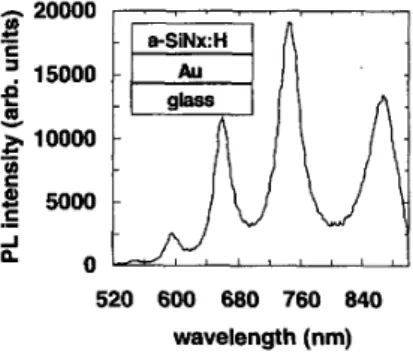
Figure 2 depicts the PL of an a-SiNx:H mi- crocavity formed with a metallic Au back mir- ror. The PL is modulated by the strong Fabry- Perot resonances, which have linewidths of AA
= 25 nm and quality factors of Q = 30. The mode number of these resonances were found to range from m = 11 ( A l l = 558 nm) to m = 7 (A, = 874 nm). Although the metallic mirror microcavity reduces the gain linewidth from 240 nm to 25 nm for an individual resonance, there are still multiple resonances within the gain region.
In order to reduce the linewidth further and increase spectral purity, we decided to use a VCSEL structure a-SiNx:H microcavity with
5000 0 CI
-
5
4000 n Y3
3000E
-2
2000-
E
1000 a, 4 520 600 680 760 840 wavelength(nm)
JFA5 Fig. 1. PL spectrum of the 1400 nm thick Si rich a-SiN,:H grown on a glass substrate.
h 20000 15000
.-
3
@
2
10000 CJ
.-
(R5
5000-
4n
o
520 600 680 760 840 wavelength(nm)
JFA5 Fig. 2. PL spectrum of the 1400 nm thick Si rich a-SiN,:H grown on the 100 nm thick Au mirror.
528
/
CLEO’99
/
FRIDAY
MORNING
4-.-
5
4000d
v 3000E
-9
2000.-
c
1000 Ai
520 600 680 760 840 wavelength (nm) JFA5 Fig. 3. PL spectrum of the Si rich a- SiN,:H grown in between the top and bottom DBRs.dielectric DBRmirrors. The DBR mirrors were fabricated using 4 pairs of quarter wavelength thick (A/4n) Si rich a-SiNx:H (with n1 = 2.1) and N rich a-SiNx:H with (with n2 = 1.6) at A
= 740 nm (gain maximum). The thickness of the Si rich a-SiNx:H microcavity (in between the DBR’s) is equal to A/2n,. Figure 3 depicts the PL of the a-SiNx:H microcavity formed with the dielectric DBR mirrors. The strong Fabry-Perot resonance has AA = 6 nm and Q = 123. The width of the rejection band is 200 nm.
‘Florida International University, Physics De- partment, University Park, Miami, Florida
331 99 USA; E-mail: [email protected]
1. L. Pavesi, R. Guardini, and C. Mazolleni,
Solid State Commun. 97, 1051 (1996). 2. A. Aydinli, A. Serpengiizel, and D. Vardar,
Solid State Commun. 98,273 (1996). 3. A. Serpenghzel, A. Aydinli, and A. Bek,
OpticsExpress 1, 108 (1997).
4. A. Serpengiizel, A. Aydinli, A. Bek, and M.
Giire,
I.
Opt. Soc. A m . B 15,2706 (1998).JFA6 9:30 am
Enhanced light amplification due to groupvelocity anomaly in
two-
dimensional photonic crystals Kazuaki Sakoda, Research Institute for Electronic Science, Hokkaido University, Kita
12-jo Nishi &home, Kita-ku, Sapporo 060-
0812, Japan
Photonic crystals can control the nature of radia- tion field.’ In addition to their peculiar optical properties such as suppression of spontaneous emission due to photonic band gaps, the small group velocity at band edges and so on, which
will be called group-velocity anomaly hereafter,
brings about the enhancement ofsun-frequency generation* and stimulated emi~sion.~.~ In this paper, we will derive an analytical expression for the enhancement of light amplification and evaluate it numerically for two-dimensional crystals with finite thickness to show that an ex- tremely large enhancement can be observed even for very
thin
samples.We assume that impurity atoms with in- verted population are embedded in a photonic crystal. By means of the Green’s-function method,* we can show that the amplitude am- plification factor of light in a unit lengthfk, is
w a 2 n c
-
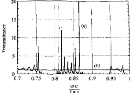
JFA6 Fig. 1. The transmission spectra of (a) the two-dimensional triangular photonic crystal and (b) a uniform plate with the spatially averaged dielectric constant and the same thickness. We should note that the transmittance may be larger than unity because of the stimulated emission accompanied by the negative imaginary part of the dielectric constant.
inversely proportional to the group velocity of
the radiation mode ug(kp):
where
k
and p denote the wave vector in the first Brillouin zone and the band index, wkP is the eigen-angular-frequency of the radiation mode, a is the polarizability of the impurity atoms, and F(kp) is given by the following equation.In Eq. (2), V,, denotes the unit cell, n(r) is the density of the impurity atoms, and Ekp(r) is the normalized eigenfunction of the electric field. On the other hand, fkb can be evaluated by calculating the transmission spectra of the as- sumed sample. Figure 1 shows an example of the transmission spectrum of a two- dimensional triangular photonic crystal com- posed of eight layers of cylindrical air holes formed in PbO glass, which was calculated by the plane-wave expansion method.5 In Fig. 1,
w, a, and c denote the angular frequency, the lattice constant, and the light velocity in vacuum. Following parameters were used for the numerical calculation: R / a = 0.42 and E = 2.72-0.01i, where R is the radius of the cylin- drical holes and E is the dielectric constant of PbO. The negative imaginary part of the di- electric constant was assumed to model the inverted population of the impurity atoms dis- persed uniformly in PbO. A large enhance- ment of transmittance with interference pat- terns is clearly observed in Fig. 1. We will show that this enhancement is really related to the group-velocity anomaly.
1. J.D. Joannopoulos, R.D. Meade, and J.N.
Winn, Photonic Crystals (Princeton Uni- versity Press, Princeton, 1995).
K. Sakoda and K. Ohtaka, Phys. Rev. B 54, 5732 (1996); ibid. 5742.
J.P. Dowling etaL, J. Appl. Phys. 75, 1896 (1994).
S . Nojima, Jpn. J. Appl. Phys. 2, Lett. 37, L565 (1998).
2. 3.
4.
5. K. Sakoda, J. Opt. SOC. Am. B 14, 1961 (1997).
JFA7 9:45 am
Semiconductor quantum-dot photonic crystals
Yu. A. Vlasov, Nan Yao,* D.J. Norris,** NEC Research Institute, 4 Independence Way, Princeton, New Jersey 08540 USA; E-mail: vlasov@research. nj. nec.com
Here we show how to use self-organization to make three-dimensional semiconductor pho- tonic crystals operating at optical wavelengths. Our approach combines colloidal chemistry with two steps of hierarchical self-assembly. First monodisperse submicron silica spheres slowly settle onto a flat substrate and self- organize as a (mostly) face-centered cubic (fcc)
lattice that is periodic on an optical length scale. Second, this template serves as a three- dimensional scaffolding for the self-assembly of nanometer-scale CdSe colloidal quantum dots. Subsequently, the silica template is re- moved by selective etching and a three- dimensionally patterned material consisting solely of densely-packed semiconductor quan- tum dots is obtained. Therefore, the exact three-dimensional structure of the template is imprinted in the final material.
The resulting material is particularly inter- esting as a photonic crystal since we control several key parameters, which determine its final behavior. First, we control the unique optical properties of individual semiconductor quantum dots. They have discrete optical tran- sitions, efficient luminescence, high gain and optical nonlinearities, which are tunable with the size of the nanocrystal. Second, we control
how the individual nanocrystals interact with each other. When quantum dots self-assemble into densely-packed arrays, referred to as quantum-dot solids, the collective electronic and optical behavior of the solid strongly de- pends on the spacing and arrangement of the nanocrystals. By modifying this secondary structure of the nanocrystals, we can optimize this collective behavior in the macroporous solid. Finally, we control the structure of the silica template. By adjusting the size, spacing, and arrangement of the silica spheres, we de- termine how the quantum-dot solid is pat- terned on an optical-length scale. This tertiary structure modifies the internal electro- magnetic environment and influences the propagation of photons through the material. Furthermore, due to the melting point de- pression of nanometer-scale particles, the densely-packed nanocrystals can be sintered to form a bulk semiconductor solid at relatively low temperatures. This opens a general and inexpensive route to three-dimensional semi- conductor photonic crystals that possess ex- tremely high refractive index contrast. Here we demonstrate our method by preparing three- dimensionally patterned bulk CdSe. Accord- ing to theory, obtained refractive index con- trast (2.86 at 720 nm) is sufficient to open a small, but complete, photonic bandgap at op- tical wavelengths. Future work will explore this intriguing possibility.