1. Introduction
Integrated circuits (ICs) have witnessed a unique improve-ment in functionality and performance through downscaling, while significant challenges lie ahead for keeping up the pace of miniaturization [1]. Semiconductor manufacturing is marching toward three-dimensional (3D) ICs to over-come complexity of miniaturization in conventional planar devices [2], where batch fabrication of multiple length scales is the immediate challenge. A similar development is taking place in micro electromechanical systems (MEMS), where
new-generation physical sensors exploit the mechanical sen-sitivity brought by the introduction of piezoresistive silicon nanowire (Si NW) gages into conventional MEMS architec-ture [3, 4]. With a two-order-of-magnitude difference between the MEMS layer thickness and the critical dimension (CD) of the Si NW, the associated setting is inherently 3D. In addi-tion to their role as stress concentraaddi-tion elements leading to elevated mechanical sensitivity in MEMS, Si NWs have fur-ther significant advantages such as overcoming signal losses and increasing resonance frequency, two features already widely used in nano electromechanical systems (NEMS). Si NWs obtained via bottom-up techniques provide a high mechanical quality factor, Q, and are also reported to exhibit
Journal of Micromechanics and Microengineering
Piezoresistive silicon nanowire resonators
as embedded building blocks in thick SOI
Mohammad Nasr Esfahani1,5 , Yasin Kilinc1,5, M Çagatay Karakan2,Ezgi Orhan2, M Selim Hanay2, Yusuf Leblebici3 and B Erdem Alaca1,4
1 Department of Mechanical Engineering, Koç University, Rumelifeneri Yolu, 34450 Sariyer, Istanbul, Turkey 2 Department of Mechanical Engineering and UNAM, Bilkent University, 06800 Bilkent, Ankara, Turkey 3 Microelectronic Systems Laboratory, EPFL, Bldg ELD, Station 11, CH-1015 Lausanne, Switzerland 4 Surface Science and Technology Center, Koç University, Rumelifeneri Yolu, 34450 Sariyer, Istanbul, Turkey
E-mail: [email protected]
Received 2 November 2017, revised 26 December 2017 Accepted for publication 29 January 2018
Published 15 February 2018 Abstract
The use of silicon nanowire resonators in nanoelectromechanical systems for new-generation sensing and communication devices faces integration challenges with higher-order structures. Monolithic and deterministic integration of such nanowires with the surrounding microscale architecture within the same thick crystal is a critical aspect for the improvement of
throughput, reliability and device functionality. A monolithic and IC-compatible technology based on a tuned combination of etching and protection processes was recently introduced yielding silicon nanowires within a 10 µm-thick device layer. Motivated by its success, the implications of the technology regarding the electromechanical resonance are studied within a particular setting, where the resonator is co-fabricated with all terminals and tuning electrodes. Frequency response is measured via piezoresistive readout with frequency down-mixing. Measurements indicate mechanical resonance with frequencies as high as 100 MHz exhibiting a Lorentzian behavior with proper transition to nonlinearity, while Allan deviation on the order of 3–8 ppm is achieved. Enabling the fabrication of silicon nanowires in thick silicon crystals using conventional semiconductor manufacturing, the present study thus demonstrates an alternative pathway to bottom-up and thin silicon-on-insulator approaches for silicon nanowire resonators.
Keywords: silicon nanowire, nanowire resonator, piezoresistive readout, top-down fabrication, semiconductor manufacturing, NEMS
(Some figures may appear in colour only in the online journal)
M N Esfahani et al
Piezoresistive silicon nanowire resonators as embedded building blocks in thick SOI
Printed in the UK 045006 JMMIEZ © 2018 IOP Publishing Ltd 28 J. Micromech. Microeng. JMM 10.1088/1361-6439/aaab2f
Paper
4Journal of Micromechanics and Microengineering IOP
5 These authors contributed equally to this work 2018
1361-6439
https://doi.org/10.1088/1361-6439/aaab2f
[14–16]. For the cases where the Si NW has to be attached to a much thicker MEMS device, a similar approach is adopted, where the nanoscale component is fabricated in thin silicon on insulator (SOI) first. This is then followed by the deposition of a 10 µm-thick structural Si layer dedicated to MEMS fabrica-tion [4]. This multiscale technique is shown to work well in applications such as 3D inertial sensors [4], magnetometers [17] and gyroscopes [18].
Si NWs can also be obtained within the same thick Si crystal as the rest of microscale device. For example, Si NWs can be obtained in bulk Si through using an oxide encapsulation around a nanoscale protrusion followed by a plasma etching process for release [19]. An alternative approach employs Ga+ doping by focused ion beam (FIB) imparting etch selectivity to the doped region. A subsequent etching process releases Si NWs attached to microscale terminals [20, 21]. A more recent study reports the co-fabrication of Si NWs with MEMS by tuning the involved deep etch (DRIE) process such that fine scallops define a nanoscale beam, while subsequent coarse scallops release it and simultaneously generate MEMS [22].
Although top-down techniques based on semiconductor manufacturing provide the most promising pathway for on-chip integration with parallel processing capability and dimensional control [23], the following disadvantages associ-ated with the aforementioned technologies remain:
(i) In the early example of oxide protection, intensive etch rate in the protective layer limits the etch depth to a very shallow trench. Therefore, the challenges of preserving Si NWs in plasma etching impose thickness uniformity issues via RIE [19]. Although isotropic release is reported recently with sidewall passivation through C4H8 as well, a similar difficulty to retain the Si NW in plasma etching confines the ultimate etch depth for a minimum Si NW thickness. An ultimate trench depth of 3 µm for a released Si NW with a CD of about 500 nm is reported [24]. (ii) A more recent example employs a much thicker initial
protrusion instead of sidewall passivation defined in etch cycles with fine scallops. This is then followed by etching with coarse scallops for an isotropic release. While a subsequent oxide thinning reduces the sidewall roughness and the Si NW cross-section, preserving sub-micron trench width—specially in MEMS devices—and inducing residual stresses at high temperatures are the
co-fabricated [26–29]. This is achieved through a combina-tion of high-resolucombina-tion lithography and a two-step etching process. The first shallow etch creates a nanoscale protrusion on the surface, which is then released through the isotropic etch comp onent of the following DRIE. Although this final etch depth is very large compared to the CD of the Si NW, protective layers around the Si NW in addition to the appro-priate DRIE recipe proved to work well. Si NWs are not attacked along their unprotected bottom surface. In the first demonstration, the technique delivers Si NWs with a CD of 35-nm spanning at least 10 µm-deep trenches [28]. Recently, this monolithic technology is improved for the integration of Si NWs with microscale architectures with an extreme trench depth of 40 µm [26].
Although the applicability of this new technology to the piezoresistive measurement of small forces was also recently demonstrated utilizing MEMS [3], it was realized only under quasistatic conditions. The present study is the first report of the resonance behavior of such piezoresistive Si NWs obtained in thick SOI substrates. Electrostatic actuation and piezoresistive readout are utilized. Resonance behavior is characterized for a NW geometry embedded within a 10 µm-thick device layer. In the remainder of the paper, architecture and preparation of suspended Si NWs between microscale ports are introduced first. The device is intended to operate as a mechanical reso-nator with piezoresisive transduction. Frequency response for first and second modes is analyzed using frequency down-mixing technique. The electromechanical characterization is followed by studying nonlinearity and frequency stability. The work is concluded by introducing the applications of the technique for new-generation sensors and power-efficient ICs through addressing the shortcomings associated with avail-able bottom-up and thin-SOI technologies.
2. Device architecture and sample preparation
The device is designed based on a suspended piezoresistive Si NW electromechanical resonator spanned between microscale electrodes. One lateral gate induces a mechanical vibration in the double-clamped Si NW. The piezoresistive behavior of the highly-doped Si NW provides the transduction between mechanical and electrical domains. Fabrication technique is developed on a 100 mm-diameter, highly doped 1 0 0 SOI wafer with a 10 µm-thick device layer, a 1 µm-thick
buried oxide (BOX), and a 380 µm-thick handle layer. The wafer is doped with phosphorous to a mean resistivity of
5 × 10⁻⁴Ω· cm. A high-resolution lithography defines the Si NW width, while the subsequent reactive ion etching (RIE) process sets the Si NW thickness. Fabrication details can be found elsewhere [26, 28, 29]. It should be emphasized that this technique yields Si NWs on the top surface of the SOI device layer, in which other microscale features are generated in the same batch by preserving an up to two-order-of-magnitude scale difference. This scale-up integration has been possible thanks to a combination of different etching steps while pro-tecting the rather fragile Si NW.
One such Si NW between two lateral electrodes is shown in figure 1(a). A gap of 400 nm between the Si NW and electrodes is achieved corresponding to a trench aspect (depth-to-width) ratio of 25. Frequency response of the device is characterized based on the frequency down-mixing approach. The high-frequency signal from the mechanical motion, ωc,
of the resonator is converted to a lower frequency, ωL, to be detected by a lock-in amplifier. The frequency response is measured based on the two source-1ω detection mechanism, having resistance changes proportional to the Si NW deflec-tion [30]. In this technique, Si NW is at excitation frequency,
VNW,1ω=VNWAC cos(ωc),while the gate has a small offset,
Vgate,1ω=VgateAC cos(ωc+ ωL), (figure 1(b)). Measurement is carried out at different pressure levels to verify the mechan-ical nature of the resonance, further facilitating an appropriate Figure 1. (a) Si NW resonator along 1 0 0 with a 5 µm length,
100 nm width and 200 nm thickness surrounded by two electrostatic gates with a gap of 400 nm. False color in yellow represent metal pads. (b) Schematic diagram of the measurement circuit. LIA: lock-in amplifier, BT: bias tee, LPF: low-pass filter, HPF: high-pass filter.
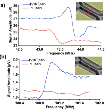
Figure 2. (a) First-mode frequency response of the device at drive NW voltage VAC
NW=0.4 V and driving bias voltage VgateAC =6 V at a DC level of VDC
gate=6 V at the atmospheric pressure and a pressure of 4 × 10⁻³ bar, (b) Second-mode frequency response of the device at drive NW voltage VAC
NW=0.4 V and driving bias voltage VAC
gate=10 V at a DC level of VgateDC =15 V at the atmospheric pressure and a pressure of 4 × 10⁻³ bar. (All AC voltages are expressed in terms of the peak-to-peak magnitude).
Figure 3. (a) First-mode, and (b) Second-mode electromechanical resonance for various bias voltages, VDC
gate, at a drive voltage of VAC
NW=0.4 V and a driving bias voltage of VgateAC =6 V measured at a pressure of 4 × 10⁻³ bar and room temperature. (All AC voltages are expressed in terms of the peak-to-peak magnitude).
comparison with the literature. A vacuum chamber is used, where one can work at the minimum pressure level smaller than 10−9 bar. Furthermore, the temperature of the sample
holder can be decreased to 100 K. Dice with Si NW resonators are wire-bonded to PCB for further electrical connections.
3. Results and discussion
Measurements are first taken at two different pressure levels of 1 bar and 4 × 10⁻³ bar. Frequency sweeps around the first and second modes of the Si NW are shown in figures 2(a) and (b), respectively. Curve fitting is carried out based on the Lorentzian function. The resonance peak is detected at 43.69 MHz for the first mode and 101.03 MHz for the second mode. Q values of approximatley 100 and 250 are obtained for the first mode at the atmospheric pressure and in vacuum, respec-tively. Q obtained at the atmospheric pressure is comparable to those reported for other top-down Si NWs on thin SOI [31]. The increase of Q obtained through the reduction of the pres-sure verifies the mechanical nature of the signal. Considering the oxide encapsulation around the Si NW with a trapezoidal cross-section [26, 28, 29], a finite element analysis for the frequency response of the resonator architecture yields a reso-nance frequency of 47.09 MHz and 100.98 MHz for the first and second modes, respectively. Vibration directions are also indicated by arrows in the insets in figure 2.
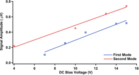
Frequency response for different gate bias voltages, VDC gate, is obtained through sweeping VDC
gate. Results are depicted in figure 3. For the first mode, increasing the bias voltage from 9 V to 15 V changes the signal amplitude from 0.25 µV to 0.51
µV improving Q from 290 to 340 at the pressure of 4 × 10⁻³ bar (figure 3(a)). Second-mode peaks for the same device can be seen in figure 3(b). An increase in signal amplitude from 0.21 µV to 0.74 µV is observed by sweeping VDC
gate from 4 V to 15 V changing Q from 280 to 330. While Q values are com-parable to those of some of the Si NW resonators obtained on thin substrates [25, 32], it also exhibits deviations, sometimes up to one order of magnitude, with the rest of the top-down [11–13, 19] and bottom-up [8, 30] technologies. At this point it is important to note that the measurement pressure
is considerably higher compared to high-vacuum condi-tions. Finally, a linear dependence of the signal amplitude on the bias voltage is observed for both modes as depicted in figure 4. This observation is a sign of the Lorentzian nature of the mechanical resonance, as the linear piezoresistive trans-duction in 1ω-detection technique yields a resistance change
proportional to the Si NW deformation [8, 33].
Furthermore, a nonlinear transition in the first mode is achieved by increasing VDC
gate up to 10 V at a sample holder temperature of 100 K and pressure <1 × 10⁻⁹ bar (figure 5). Increasing bias voltage from 3 V to 10 V changes the signal amplitude from 2 µV to 8.4 µV with a shift in the resonance frequency from 45.43 MHz to 45.65 MHz. This transition changes Q from 700 to more than 1000. A nonlinear behavior in Si NW resonator with mechanical hardening similar to those reported on thin SOI [34] is achieved providing a large dynamic motion for high-resolution sensing and signal pro-cessing applications. The nonlinearity can be characterized through using the critical response amplitude [34]. The solid red line shows the fitting peaks of resonant curves based on the obtained resonance frequency and Q in linear regime. The Lorentzian fits in linear vibration are demonstrated as dashed lines in the inset to figure 5. Further studies on the role of the readout scheme involving down-mixing in addition to the semiconductor nature of the resonator can shed light on the deviation present in the background fit. We also note that the field effect arising from the electrostatic actuation could mod-ulate the resistance, while this effect for the highly-doped Si NW of this work is negligible [3, 26]. Hence, the modulated resistance in the Si NW is a direct result of the mechanical strain induced during resonance.
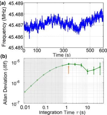
Frequency stability (Allan deviation) measurement is car-ried out as well for the first-mode (figure 6). A fractional frequency fluctuation on the order of 3–8 ppm is achieved. As a mass sensor this resonator with an effective mass in the order of Meff≈ 170 fg would offer a mass resolution of δM ≈ 1.0 ag. The Allan deviation obtained in this study is comparable to those reported by previous top-down techniques for high-resolution detection [11, 12]. This stability can be improved through further size reduction in cross-section and surface improvement of Si NWs for achieving higher Q [35].
Figure 4. The linear variation of the signal amplitude with DC bias voltage, VDC gate.
The proposed monolithic integration of the Si NW with the surrounding microscale architecture within the same Si crystal eliminates assembly drawbacks related to bottom-up approaches. As discussed earlier in Introduction it also elimi-nates a series of complications and restrictions associated with available top-down techniques. In this work this point is demonstrated for the case of electromechanical resonators. Based on standard IC-compatible processes, the fabrication technology is shown to deliver Si NW electromechanical reso-nators within a thick substrate with a two-order-of-magnitude scale difference between the Si NW and the surrounding archi-tecture. Operation frequencies demonstrated are in the order of
those reported in thin SOI [11–13], trench etching [14, 19, 25] and bottom-up [8, 30] studies. The obtained Q for embedded Si NW resonator in thick SOI is also found to be comparable to those of several top-down reports [25, 31, 32]. This approach provides a frequency stability in a similar range to that reported by thin-SOI work [11, 12]. Furthermore, the presented tech-nology demonstrates the tuning to nonlinearity by electrostatic mechanism similar to available approaches [8, 32, 34] facili-tating large dynamic motion in Si NW resonators embedded in thick substrates for new-generation sensing and communica-tion devices. The essential features of the suspended Si NW resonator in thick SOI is summarized in table 1.
The present study addresses the integration of Si NW resona-tors with higher-order structures in modern electronic devices [17, 36]. Implementation of in situ actuation and readout in electromechanical resonators can also enable the incorpora-tion of large resonator arrays in very-large scale integraincorpora-tion (VLSI) [9, 11]. Resonance can further be improved through downscaling the Si NW cross-section, controlling doping level for higher piezoresistive gage factors [5, 6] and reducing the surface roughness [35]. The e-beam lithography step imposes a sidewall and line edge roughness that can be reduced through proximity effect correction technique [26]. In the present tech-nology, the size reduction can be carried out by the definition of initial protrusions via lithography and shallow etch steps to decrease the width and the thickness of the Si NW, respectively [3, 28, 29]. A diffusion technique is utilized to dope the Si top surface to a mean resistivity of 5 × 10⁻⁴ Ω· cm to prevent any electrical contact issues [3, 26]. However, a higher level of resistivity is required to yield the optimum gage factor [5]. Figure 5. Linear to nonlinear transition in the first mode for a series of bias voltages, VDC
gate, between 3 V to 10 V at a drive voltage of VAC
NW=0.4 V and a driving bias voltage of VgateAC =10 V measured at a pressure of 2 × 10⁻¹² bar and stage temperature of 100 K. (All AC voltages are expressed in terms of the peak-to-peak magnitude). The solid red line indicates the mechanical nonlinearity response. Linear resonance is shown in the inset. The red dashed line in the inset is a Lorentzian fit.
Figure 6. (a) Frequency versus time, (b) Allan deviation as a function of the integration time taken at 100 K stage temperature, under a pressure of 2 × 10⁻¹² bar. With the arrow in (b) indicating the response time of the PLL, values for shorter time scales do not reflect the actual unstability.
Table 1. Features of the Si NW resonator embedded in thick SOI.
Q f (MHz) (fg)Meff δM(ag) δf /f(ppm) 1 (bar) 4 × 10 −3 (bar) <1 × 10⁻⁹ (bar) First- mode
Second-mode 170 1.0 3–8
preserved. While a nearby gate is used for electrostatic actua-tion, the piezoresistivity of the Si NW resonators is utilized for the readout, resulting in an on-chip, 3D resonator architec-ture. Using frequency down-mixing technique the mechanical nature of resonance with frequencies as high as 100 MHz is verified through both pressure damping and the transition to nonlinearity. The overall operation of suspended Si NW resonators in thick substrate is comparable to those reported through available top-down, including thin SOI and trench etching, technologies. By addressing deficiencies related to the available bottom-up and top-down SOI technologies for delivering similar electromechanical resonators, the present work provides a monolithic technology for new-generation sensors and 3D-ICs in modern electronic devices.
Acknowledgment
The authors gratefully acknowledge the support by Tubitak under Grant no. 112E058. MNE was supported by the Tubitak- BIDEB 2216. This work was also supported by ISTKA under Grant TR10/16/YNY/0103 ‘Nanotechnology Platform for the Accessible and Sustainable Pilot Fabrication of High-Added-Value Products’.
ORCID iDs
Mohammad Nasr Esfahani https://orcid.org/0000-0002- 6973-2205
B Erdem Alaca https://orcid.org/0000-0001-5931-8134 References
[1] Thompson S E and Parthasarathy S 2006 Mater. Today 9 20–5
[2] Lau J H 2014 J. Electron. Packag. 136 040801
[3] Esfahani M N, Leblebici Y and Alaca B E 2017 J. Microelectromech. Syst.26 624–31
[4] Robert P, Nguyen V, Hentz S, Duraffourg L, Jourdan G, Arcamone J and Harrisson S 2009 M&NEMS: a new approach for ultra-low cost 3d inertial sensor IEEE Sensors (IEEE) pp 963–6
[5] He R and Yang P 2006 Nat. Nanotechnol. 1 42–6
[6] Schmidt V, Wittemann J V, Senz S and Gösele U 2009 Adv. Mater.21 2681–702
[7] He R, Gao D, Fan R, Hochbaum A I, Carraro C, Maboudian R and Yang P 2005 Adv. Mater. 17 2098–102
[8] He R, Feng X, Roukes M and Yang P 2008 Nano Lett.
8 1756–61
[15] Boodhoo L, Crudgington L, Chong H M, Tsuchiya Y,
Moktadir Z, Hasegawa T and Mizuta H 2015 Microelectron. Eng.145 66–70
[16] Rahman S, Yusof N, Hamidon M, Zawawi R and Hashim U 2014 Top-down fabrication of silicon nanowire sensor using electron beam and optical mixed lithography IEEE Int. Conf. on Semiconductor Electronics (IEEE) pp 64–7
[17] Ettelt D, Rey P, Jourdan G, Walther A, Robert P and Delamare J 2014 J. Microelectromech. Syst. 23 324–33
[18] Walther A, Savoye M, Jourdan G, Renaux P, Souchon F, Robert P, Le Blanc C, Delorme N, Gigan O and Lejuste C 2012 3-axis gyroscope with si nanogage piezo-resistive detection IEEE 25th Int. Conf. on Micro Electro Mechanical Systems (IEEE) pp 480–3
[19] Cleland A N and Roukes M L 1996 Appl. Phys. Lett.
69 2653–5
[20] Chekurov N 2011 Fabrication process development for silicon micro and nanosystems PhD Thesis Aalto Univeristy, Helsinki
[21] Henry M D, Shearn M and Scherer A 2010 J. Vac. Sci. Technol. B 28 C6F26–30
[22] Tsuchiya T, Hemmi T, Suzuki J Y, Hirai Y and Tabata O 2016 Proc. Struct. Integrity2 1405–12
[23] Singh R 2015 IEEE Electron Devices Soc. Newsl. 22 13–4 [24] Wei J, Magnani S and Sarro P M 2012 Sensors Actuators A
186 80–5
[25] Llobet J, Sansa M, Gerbolés M, Mestres N, Arbiol J, Borrisé X and Pérez-Murano F 2014 Nanotechnology
25 135302
[26] Esfahani M N, Yilmaz M, Wollschläger N, Rangelow I W, Leblebici Y and Alaca B E 2017 Microelectron. Eng. 183
42–7
[27] Tasdemir Z, Peric O, Sacchetto D, Fantner G E, Leblebici Y and Alaca B E 2015 IEEE Nanotechnol. Express 1 2–5
[28] Tasdemir Z, Wollschläger N, Österle W, Leblebici Y and Alaca B E 2016 Nanotechnology 27 095303
[29] Yilmaz M, Kilinc Y, Nadar G, Tasdemir Z, Wollschläger N, Österle W, Leblebici Y and Alaca B E 2017 J. Vac. Sci. Technol. B 35 022001
[30] Sansa M, Fernández-Regúlez M, San Paulo Á and Pérez-Murano F 2012 Appl. Phys. Lett. 101 243115
[31] Ollier E et al 2012 Ultra-scaled high-frequency single-crystal si nems resonators and their front-end co-integration with cmos for high sensitivity applications IEEE 25th Int. Conf. on Micro Electro Mechanical Systems (IEEE) pp 1368–71
[32] Bartsch S T, Arp M and Ionescu A M 2014 IEEE J. Electron Devices Soc.2 8–15
[33] Sansa M, Fernández-Regúlez M, Llobet J, San Paulo Á and Pérez-Murano F 2014 Nat. Commun. 5 4313
[34] Kozinsky I, Postma H C, Bargatin I and Roukes M 2006 Appl. Phys. Lett.88 253101
[35] Ekinci K and Roukes M 2005 Rev. Sci. Instrum. 76 061101
[36] Choudhury D 2010 3d integration technologies for emerging microsystems IEEE MTT-S Int. Microwave Symp. Digest (IEEE) pp 1–4