ί г i
D E S
íQ
tí a n d t e s t i n g o f aQ PñO C E SSO ñ COIV
îP
âT İB L
c1·2β-8ΙΤ
C O K ñH LA TO R C H IP
іЛ. TD ·. ¿ D T.-А А .D JÍAwiK
Vs
5 S- CV.-ir·'/·
DESIGN AND TESTING OE A
MICROPROCESSOR COMPATIBLE
128
-BIT
CORRELATOR CHIP
A T H E S I S S U B M I T T E D T O T H E D E P A R T M E N T O F E L E C T R I C A L A N D E L E C T R O N I C S E N G I N E E R I N G A N D T H E I N S T I T U T E O F E N G I N E E R I N G A N D S C I E N C E S O F B I L K E N T U N I V E R S I T Y IN P A R T I A L F U L F I L L M E N T O F T H E R E Q U I R E M E N T S F O R T H E D E G R E E O F M A S T E R O F S C I E N C EBy
Satılmış Topçu
July 1989
'TVíti^ 'ΎΥ.
I certify that I have read this thesis and that in my opinion it is fully adequate, in scope and in quality, as a thesis for the degree of Master of Science.
Assoc. Prof. Dr. Abdullah Atalar(Principal Advisor)
I certify that I have read this thesis and that in my opinion it is fully adequate, in scope and in quality, as a thesis for the degree of Master of Sconce.
Assoc. Prof. Dr. Levent Onural
I certify that I have read this thesis and that in my opinion it is fully adequate, in scope and in quality, as a thesis for the degree of Master of Science.
4 ^ / i l l
Asst. Prof. Dr. Mehm' an
Approved for the Institute of Engineering and Sciences:
ABSTRACT
DESIGN AN D TESTING OF A MICROPROCESSOR
COMPATIBLE 128-BIT CORRELATOR CHIP
Satılmış Topçu
M.S. in Electrical and Electronics Engineering
Supervisor: Assoc, Prof. Dr. Abdullali Atalar
July 1989
In digital synchronous data transmission, synchronization (sync) words are used to mark the beginning of the incoming data stream. Detection of the sync word received from a noisy channel is a difficult problem. One of the optimum solutions to this problem is to use a correlator. A correlator could be implemented with SSI and MSI components on a printed circuit board with the disadvantage of bulkiness. To use it in light-weight equipment such as portable data terminals, it is designed to be implemented as a full-custom single VLSI chip. It can be used for the 128-bit sync word detection and PRBS generation. Two chips can be cascaded for 256-bit correlation as well as distributed sync words, and inverted or non-inverted sync words can be detected. It is fully programmable by a microprocessor to set the number of tolerable errors in detection and to select the bits of the 128-bit (or 256-bit) input data stream to be used in the correlation and hence, it can be directly connected to a microprocessor as a peripheral device.
In designing the correlator chip some Design For Testability methods are used to improve the testability. Especially, scan design and partitioning tech niques are applied resulting in a significant decrease in the number of test patterns although these techniques involve an overhead in the overall tran sistor count only by 1 percent.
For functional and timing simulations E S IM and R N L simulators are used, respectively. Test patterns for the registers are generated manually
and for testing of the combinational part two programs, gen and check, are written in C programming language. The simulation programs and test pattern generation programs are run on SUN workstations under 4.3 BSD UNIX^ operating system.
Keywords: Digital synchronous data transmission, correlator, chip, VLSI, IC testing, design for testability.
ÖZET
b i r
MIKROİŞLEMCI
u y u m l u128-BIT
k o r e l a t ö rYONGASININ TASARIM I V E TEST EDİLMESİ
Satılmış Topçu
Elektrik ve Elektronik Mühendisliği Bölümü Yüksek Lisans
Tez Yöneticisi: Doç. Dr. Abdullah Atalar
Temmuz 1989
Eş zamanlı sayısal veri iletişiminde, senkron (sync) sözcüğü gelen verinin başlangıcını belirler. Gürültülü bir kanaldan alman senkron sözcüğün sezil mesi zor bir problemdir ve bu problemin en uygun çözümlerinden biri ko relatör kullanmaktır. Bir korelatör düşük ve orta yoğunluklu tümleşik dev reler kullanılarak baskılı devre üzerinde gerçekleştirilebilir, fakat büyük bir alan kaplaması olumsuz yanıdır. Bu çalışmada, taşınabilir veri terminalleri gibi hafif donanımlarda kullanılabilecek, mikroişlemci uyumlu, çok yüksek yoğunluklu tümleşik (VLSI) 128-bit programlanabilir sayısal korelatör yon gası tasarlandı. Bu korelatör yongası 128-bit uzunluğa kadar olan senkron sözcüklerini sezebilir. Ayrıca iki yonganın birbirine kademeli olarak bağlan masıyla 256-bitlik korelatör elde edilebilmektedir. Senkron sözcük, gelen verinin düz yada tersine çevrilmiş olduğu her iki durumda da sezilebilir. Ko relatör bir mikroişlemci tarafından bütünüyle programlanabilir ve bu nedenle mikroişlemciye bir çevre birimi olarak doğrudan bağlanabilir. Korelasyonda kullanılacak bitleri seçme özelliğine sahip olan korelatör, dağıtılmış senkron sözcüğü seziminde ve yalancı rasgele ikili seri (PRBS) üretiminde kullanılabi lir.
Korelatörün tasarımında bazı “test edilebilirlik tasarımı” metodları kul lanıldı. Özellikle tarama tasarımı (scan design) ve parçalama (partition ing) yöntemleri kullanılarak test vektör sayısı önemli ölçüde azaltıldı. Buna
rağmen test edilebilirlik tasarım metodları yonga tasarımına yalnızca % 1 ek transistor artışı getirdi.
Yonganın işlevsel ve zamanlama simülasyonları E S İM ve R N L simülas- yon programları kullanılarak yapıldı. Yazmaçlar için kullanılacak olan test vektörleri doğrudan elle bilgisayarda üretilmiş olup kombine mantık devreleri nin test edilmesi için de, C programlama dilinde gen ve check adlı iki prog ram yazıldı. Bu test vektörü üreten programlar ve simülasyon programları 4.3 BSD UNIX^ işletim sistemi altında SUN bilgisayar sistemlerinde çalıştırıldı.
Anahtar kelimeler : Eş zamanlı sajusal veri iletişimi, korelatör, yonga, VLSI, tümleşik devre testi, test edilebilirlik tasarımı.
ACKNOWLEDGEMENT
I would like to thank to Assoc. Prof. Dr. Abdullah Atalar for his supervision, guidance, suggestions, and encouragement throughout the development of this thesis. I am also indebted to the members of my thesis committee: Assoc. Prof. Dr. Levent Onural, Asst. Prof. Dr. M. Ali Tan, and Asst. Prof. Dr. Gürhan Şaplakoğlu for their advice and support.
A special note of thanks is due to the research assistants in VLSI group: I. Enis Ungan and Mustafa Karaman for their valuable remarks, comments, and helps. Many thanks also to Şenol Toygar who is the original designer of the correlator, to Nesip Aral, Tuncay Ergün, Oğuz Şener (all from ASELSAN) who gave their time for the improvement of the correlator system design.
I am grateful to my wife for providing morale support during this study.
TABLE OF CONTENTS
1 INTRODUCTION
1.1 Detection of Digital Signals 1.2 PRBS Generation...
1
4 1.3 The Digital Correlator2 THE ARCHITECTURE DESIGN AND OPERATION OF
THE CHIP
7
2.1 General IC Design Process... 7 2.2 S pecification s... 10 2.2.1 Specification of the F u n ction s... 10
2.2.2 Performance Requirements 11
2.2.3 System Environment and Interface D efin ition ... 11 2.3 The Architecture D esign ... 12 2.3.1 General D e s c rip tio n ... 12
2.3.2 Block Representation
12
2.3.3 Pin Description... 22 2.4 Modes of Operation 2.4.1 Correlator Mode 23 232.4.2 PRBS Generator Mode 29
3 THE LOGIC AND CIRCUIT DESIGN
31
3.1 The Logic D e sig n ... 31 3.2 The Circuit D e sig n ... 40
4 DESIGN FOR TESTABILITY
42
4.1 Ad Hoc DFT M e th o d s ... 43
4.2 Structured DFT Approaches 45
5 SIMULATIONS AND TESTING OF THE CHIP
51
5.1 Functional V erification... 51 5.2 Timing Verification... 53 5.3 Test Pattern Generation (TPG ) and Fault Simulation . . . . 55
6 CONCLUSION
63
REFERENCES
65
APPENDIX A
68
APPENDIX B
75
LIST OF FIGURES
1.1 Basic digital correlator. 3
1.2 Maximal-length linear feedback shift register... 5
2.1 The linear design process not including iterative loops... 8
2.2 Block diagram of the correlator in the beginning... 13
2.3 Simplified block diagram of the correlator... 15
2.4 Block diagram of the mask and reference registers... 16
2.5 Timing diagram of the write and read cycles... 17
2.6 Block diagram of the integrator. 20 2.7 Block diagram of the decision maker... 20
2.8 Pin diagram of the correlator... 22
2.9 Timing diagram of the sync detection... 25
2.10 128-bit correlation scheme. 26 2.11 256-bit correlator... 27
2.12 256-bit correlation scheme in the master chip... 28
2.13 The configuration for PRBS generator... 29
3.3 Decoder circuit used in the controller... 34
3.4 Logic diagram of the status register... 34
3.5 Master-slave flip-flop... 35
3.6 Schematic of the 128-bit shift register... 36
3.7 Logic diagram of the reference and mask registers... 37
3.8 Logic diagram of the threshold register... 37
3.9 Logic diagram of the comparator... 37
3.10 Logic diagram of the I ’s counter... 38
3.11 The circuit of an n-bit full-adder... 38
3.12 The 9-bit full adder circuit... 39
3.13 Transistor circuit of a compare cell... 41
4.1 Symbolic representation of a shift register latch... 46
4.2 Level sensitive scan design of the reference/mask registers. . . 47 4.3 Level sensitive scan design of the threshold register. 47 4.4 Level sensitive scan design of the status register. 48
4.5 LSSD configuration of the registers. 49
LIST OF TABLES
2.1 Function of a compare cell. 18
2.2 Function table of the controller block. 21
2.3 Selecting inodes of the correlator... 23
2.4 Decision table for the sync detection... 27
2.5 Decision table for 256-bit sync detection... 29
3.1 Function table of the buffer... 32
3.2 Truth table of a carry cell... 39
5.1 Timing simulation of the reference register... 54
5.2 Timing simulation of the sync detection... 56
5.3 Test vectors for two-bit full-adders... 60
5.4 Test vectors for three-bit full-adders... 61
1. INTRODUCTION
1.1
Detection of Digital Signals
Synchronous data transmission is more complicated than asynchronous data transmission. Because it requires a higher level of coordination between the data source and user data terminal equipment than does asynchronous data communication. In return for this inconvenience, synchronous data transfer largely eliminates the overhead of the start/stop pulses of the asynchronous method and therefore provides for more efficient data transfer.
On a synchronous data link, there are two levels of synchronization to be achieved: bit synchronization and character synchronization. Bit syn chronization refers to the adjustment of the receiving data communications equipment timing so that it “knows” at what point in time to make the de cision as to whether a 1 bit or a 0 bit is currently being received. Character or frame synchronization allows the receiving equipment to determine which bit of the received bit stream actually is the first bit in a received character or which bit actually begins the data in a data frame. Frame synchroniza tion technique is useful in situations where the data transmission (bit) rate is known and invariant, where the receiver’s clock is triggered by the clock of the transmitter or where the “receiver and transmitter” are part of the same system [1].
In general, a system can achieve and maintain frame synchronization only if the incoming data stream is interrupted periodically by a specific “start- of-frame” pattern. This pattern, transmitted at the beginning of each new frame, tells the receiver that a new frame will immediately enter the input register and must be handled accordingly.
In digital synchronous data transmission, frame synchronization is ob tained by transmitting a synchronization (sync) word to define the beginning
of the incoming data frame. Detection of the sync word received from a noisy channel is an important problem. Because, in practice, due to the noise in the channel, some bits of the incoming data stream will be altered. That is why error detection and correction techniques are used in digital data transmis sion systems. Especially, the sync word, which determines the beginning of the incoming data stream, can be lost if the channel noise is high. A powerful technique for detecting the sync word is to use a correlator [2].
Correlation techniques are used widely in communications, instrumenta tion, computers, telemetry, sonar, radar, medical and other signal processing systems. Correlation has several desirable properties, inchiding:
• The ability to detect a desired signal in the presence of noise or other signals,
• The ability to recognize specific patterns within analog or digital sig nals,
• The ability to measure time delays of known signals through various media, such as materials, the human body, RF paths, electronic circuits, etc..
Probably we use correlation daily when we compare sounds, images, or other sensations relative to other sounds, images or sensations stored in our brain. As these properties indicate, the correlation between two functions is a measure of their similarity; loosely termed, it is a comparison process. This comparison can be expressed mathematically as the correlation between two functions ui(t) and 1^2(i) [2]:
1 /■ + ^ /2
R n{T) = lim Tf; I , M t ) M i + T-+00 1 J-Tf2 dt
Here , R\2{t) refers to the coi'relation between two signals, Vi and v^. It is determined by multiplying one signal, vi(t), by the other signal shifted in time, V2{t + T), and then taking the integral of the product. Thus, correlation
involves multiplication, time shifting (or delay) and integration. Inspection of the arguments of functions v\ and V2 shows that correlation handles two
represented in discrete form, where the time scale and amplitude are quan tized into discrete steps. So, in a digital system, each signal may be a series of single bit samples where the two bit values 1 and 0 are generally interpreted as positive and negative respectively and the correlation integral is changed into a finite sum. The correlation equation in discrete form becomes [2];
= X ]
vi{k) V2(n + к)
k=—oo
Here, the indices “ i;” and “n” measure out the variables denoted by “t” and “r ” in the earlier discussion. In practice, the summation will cover finite range of values of ‘Ч·” , rather than the infinite range shown here. The range depends on the durations of the two functions and of their sampled portions.
In applications involving single bit reference and single bit data streams, multiplication is actually implemented with the exclusive-NOR (EX-NOR) function, which yields positive results (1) if the two bits (polarities) coincide and negative results (0) if they differ. If these I ’s and O’s are then summed (i.e. if the number of I ’s is calculated), then the result is a correlation score ranging from 0 (for perfect anticorrelation) to N (for perfect correlation, where N is the number of taps in the system).
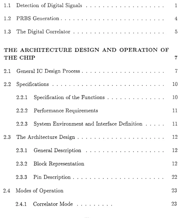
A digital correlator can perform correlation, operating according to the discrete summation equation. The major functions of a digital correlator are shown in Fig. 1.1. A reference shift register is pre-loaded with the standard synchronization pattern, while the incoming data stream is shifted serially through the input shift register. Both shift registers are n-bit long. The respective bits of the two shift registers are connected to individual exclusive- NOR gates, whose outputs are applied to a summing circuit [2].
INPUT SHIFT REGISTER
■ OUTPUT
REFERENCE SHIFT REGISTER
Figure 1.1: Basic digital correlator. 3
In operation, the correlator output is obtained by aligning the input word relative to the reference word. The respective bits in the two shift registers are compared by the exclusive-NOR gates, whose outputs are summed. The shift registers, the exclusive-NOR gates, and the summer fulfill the three functions of the correlation: time delay, multiplication, and integration, respectively. When a frame sync pattern embedded in the incoming data stream aligns exactly with the stored sync pattern, the correlator produces a sync pulse at the output, which in turn tells the receiver to start handling a new frame of data. The special start-of-frame pattern must be long and unusual to prevent false synchronization, which occurs when the correlator finds and locks onto a portion of the data stream resembling the desired synchronization pattern. The longer the sync pattern, the lower the chance of a false synchroniza tion, but the larger the percentage of the total data stream that must be dedicated to synchronization and hence is unavailable for transmitting useful information.
The receiver-correlator system operates continuously, with the correlator producing a sync pulse as it receives each successive frame sync pattern in the incoming data stream. The rate at which these pulses are generated is the frame rate of the incoming data. The correlator mainly compares the incoming data stream with a predetermined reference data and then decides whether the sync word is received or not. But, since there is a noise in the channel, the correlator must be modified in such a way that it may tolerate some number of errors in the data stream.
1.2
PR BS Generation
A pseudo-random binary sequence (PRBS) consists of a sequence of ones and zeros that possess certain specific autocorrelation properties. Such sequences play an important role in almost all types of spread-spectrum systems. One method of producing pseudo-random binary sequence is the use of feedback shift registers. These are simple to implement, are very fast in operation, and can be made to generate statistically very good sequences, provided the registers are long enough. In general, such a shift register consists of n locations labeled from 1 on the left to n on the right, which holds a binary n-string as shown in Fig. 1.2. Here, modulo 2 addition can be achieved by using exclusive-OR gates. The shift register is stepped on by shifting all the
Figure 1.2: Maximal-length linear feedback shift register.
It can be shown that the output sequence must eventually repeat with a period which is at most 2" —1. If the feedback connections have been chosen to give this maximal period, the output sequence depends on the initial contents only for its starting point (provided the initial contents are not the string of all zeros). Since the output sequences can be shown to have good quasi random properties, it seems reasonable to use them as sync words, provided n is chosen large enough and provided that the feedback is chosen to give the maximal period 2^^ — 1. The key would be to specify the feedback connections and the initial contents of the feedback shift register. In this case, the output sequence is known as a maximal-length feedback shift-register sequence.
In the correlator chip, a 128-bit shift register is used for PRBS genera tion and a single feedback line obtained from it modulo 2 summation of the selected shift register taps is applied to the serial input on the left hand side. The PRBS output is also taken serially from this feedback line instead of the output of the last stage. Here, it n is equal to 128 and it is large enough to generate very good pseudo-random binary sequences.
1.3
The Digital Correlator
Electronic systems that perform correlation have been around for years, but they have been bulky and inefficient. The development of VLSI (Very Large Scale Integration) has changed this; now correlation can be performed effi ciently with a digital correlator chip [4]. In fact, a digital correlator could be implemented with SSI and MSI components on a printed circuit board with the disadvantage of bulkiness. The continued progress in increasing the performance, speed, reliability, and the simultaneous reduction in size and cost of IC’s has made the solution easier. To use it in light-weight equip ment, such as portable data terminals, this correlator and PRBS generator was designed to be implemented as a full-custom VLSI chip. Actually, it is seen that as levels of integration go towards VLSI, the design time and design
effort needed for full-custom design technology is likely to grow exponentially. But, on the other hand, full-custom design technology offers great flexibility to the designer and it reduces circuit complexity per function and improves system performance. Also, this design technique may provide the designer an easy way of testing the chip.
The design of full-custom VLSI correlator chip was jointly carried out with I. Enis Ungan. At the beginning, we had a correlator circuit at the logic level designed by M. Şenol Toygar. Then this circuit was modified to give it some important properties such as cascade connectibility, PRBS generation, etc.. One of the main improvement is the added circuitry for testability. For this purpose, special Design For Testability (DFT) methods were used. Especially, scan design technique was applied to conti’ol the states of the registers and observe the contents of them easily by forming a scan path. Another important DFT technique used is the partitioning which reduces the problem of testing into dealing with the smaller modules. As a result, testability was improved considerably. Circuit and layout designs were done by I. Enis Ungan and so details of the circuit and layout designs can be found in [5,6].
2. THE ARCHITECTURE DESIGN AND
OPERATION OF THE CHIP
2.1
General IC Design Process
The design description for an integrated circuit may be described in terms of three domains, namely; 1) the behavioral domain, 2) the structural domain, and 3) the physical domain. A good VLSI design system should provide for consistent descriptions in all description domains and at all relevant levels of abstraction. The means by which this is accomplished may be measured in various terms that differ in importance based on the application. These design parameters may be summarized in terms of [7,8,9]
• performance - speed, power, function, • size of die,
• time to design - ease of use, and • ease of test generation and testability.
Design is a continuous trade-off to achieve adequate results for all of the above parameters. As such, the tools and methodologies used for a particular chip will be a function of these parameters. Certain end results have to be met (i.e. the chip must conform to performance specifications), but other constraints may be a function of economics or even subjectivity [10,11].
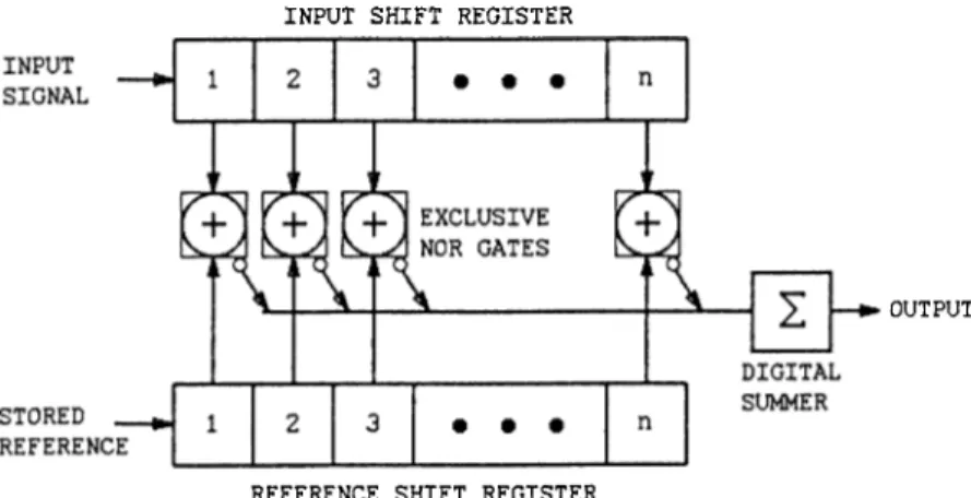
The general IC design process includes all individual steps required for designing an integrated circuit, starting with specification and ending with the generation of production control and test data. The linear design process, not including iterative loops, is shown in Fig.2.1 [12].
Mask tape Test program
It is divided in four segments, namely
1. system design, 2. logic design,
3. circuit design, and 4. layout design.
The first two segments are also often termed “logical design” , the last two “physical design” .
The system design includes the architecture and module design which, in several detailing steps, leads to logic design on the gate level. Next come the logic verification and the testability analysis. The electrical circuit design initiates the physical design with realization of logic by means of transistor circuits and subsequent verification. Finally, the layout design includes ge ometric design (i.e. the design of all masks required for production of all levels), corresponding steps of verification and, in order to establish a path to production, generation of the mask tapes. The generation of test data is based upon the logic design which results in executable test programs.
This segmentation in various levels is characteristic for IC development and shows the process from the abstract representation on a conceptual level in step-by-step realization to the mask tapes which describe in detail the manufacturing process. Each higher level constitutes an abstract represen tation of the next lower level. Vice versa, moving from a higher to a lower level requires special design know-how corresponding to the design method and technology chosen. Thus, the circuit designer has to know, for example, a way to realize the logic function of a D-fiipfiop by means of transistors and their interconnection utilizing CMOS technology.
However, it is obvious that if certain rules (design rules) have to be fol lowed, errors can be made. So, a sequence of the “implementation” and
“integration and test” steps is formed which is repeated on the various de sign levels. The repetition of the “implementation” and “integration and test” phases is required because, for each design realization, compliance with two correctness conditions has to be examined:
• Compliance with the requirements of the previous design levels, i.e. ensuring that the given target function is met by the design result obtained to that point.
• Compliance with the design rules for the actual draft of the design object on each level of representation, across the whole of the design object.
Rules pertaining to point 1 ensure vertical consistency, and rules pertaining to point 2 ensure horizontal consistency. In the case of the “layout design” step, for example, the result has to be examined with regard to consistency with the given electrical circuit design. In addition, a check of the layout design rules must be done [12].
In designing the correlator and PRBS generator chip, the general top- down method has been used following the design steps shown in Fig. 2.1. Basically, the design process includes eleven individual steps starting with specification and ending with the generation of production and test data. In the following sections, these basic design steps are presented in detail.
2.2
Specifications
Based upon a study of the requirements, the specification or performance de scription is developed by applying available techniques for problem solving. The specification includes the solution concept, functional concept, perfor mance concept and the structure concept. For the development of subsys tems, their arrangement in the main system plays a crucial role. The interface between subsystem and main system is defined by criteria such as type, for mat and range of data and command flow. For object specification including the solution concept, the performance requirements are also defined. These are, in most cases, the determination of critical time conditions, or of maxi mum values, such as the maximum current supply or the size of the memory. In the specification phase for the correlator and PRBS generator chip, af ter the specification of functions and performance requirements, the system environment and interface definition has been done [12].
2.2.1
Specification of the Functions
The correlator and PRBS generator executes the following functions:
• Two chips can be cascaded to increase the length to 256-bit.
• It allows detection of the sync regardless of the polarity of the incoming data stream.
• It can also detect distributed sync words.
• It has error tolerance utility by means of which a number of errors in the data stream can be tolerated.
• It can generate PRBS (Pseudo Random Binary Sequence).
2.2.2
Performance Requirements
Basically, the performance requirements for the correlator and PRBS gener ator chip have included the following:
• clock rate for correlation greater than 25 KHz,
• time to decide whether the sync is detected or not less than 20 /US, • clock rate for PRBS generation greater than 500 KHz,
• supply current less than 20 mA, supply voltage : 5 V.
2.2.3
System Environment and Interface Definition
The correlator and PRBS chip functions as a programmable microprocessor peripheral. So, it has an 8-bit data bus and a 3-bit address bus with chip select (CS), write (W R ), and read (RD) inputs controlled by microprocessor. Thus, its internal registers can be programmed directly through data bus of the microprocessor. The incoming data entering from the serial input (SIN) is taken inside the chip serially by using the clock (CLK) supplied by phase lock loop (PLL) and go out from the serial output (SOUT). When the sync is detected, the chip informs microprocessor by sending an interrupt signal’, which we call the sync pulse, through sync (SYN) output. In addition, the chip has an 8-bit bidirectional bus making possible 256-bit correlation by means of cascade connection of two chips.
2.3
The Architecture Design
2.3.1
General Description
The architecture design is a first approach to meet the specification require ments. The realization or actual development begins with this design phase. As usual, a top-down method is applied. The system function is divided into hierarchical levels from top to bottom. It is divided into single functions which are placed in a static connection structure, and whose interactions are controlled by means of a dynamic cooperation structure. Connection and cooperation structures are called function structures. The cooperation struc ture consists in turn of two components: one for the information flow, and one for the control flow.
In the architecture design phase, far-reaching assessments are made, such as the formal representation of system functions (target functions), division into subfunctions by hierarchically layered resolution, design of interface ar chitecture, connection structure and functional structure. For complex prob lems such decisions cannot, in general, be made with certainty. Wrong de cisions and design errors in this phase cause especially undesirable effects. So, on the various levels of the architecture design, verification steps are per formed repeatedly (architecture verification). These steps have been carried out manually for the first design outlines, as design reviews or walk-throughs
[
12
].2.3.2
Block Representation
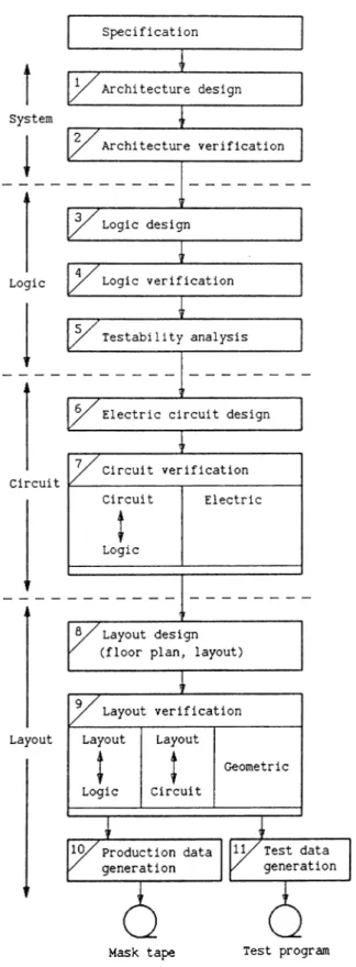
In the beginning of the architecture design, the correlator circuit designed by M. Şenol Toygar was used [13]. The block diagram of this circuit is shown in Fig. 2.2. It has some unnecessary features as well as some missing and important properties. For example, it has a PW O (Power Okey) input which will put the data bus in high-Z state when the power supply of the microprocessor is down. It has also lACS and SACS bits which control the active position of INV and SYN outputs, respectively. In addition, it has an SYN output pin. These features were thought as unnecessary and they were omitted from the design. Afterwards, the design was changed to have some important properties. For this purpose, firstly, cascade connection property was added to it in order to have the ability of performing 256-bit correlation.
Figure 2.2: Block diagram of the correlator in the beginning.
Due to this cascade connection property, 8 pins were added to be able to transfer the intermediate 128-bit correlation score at the I ’s counter output from one chip to the other. Later, PRBS generation was made possible by forming a synchronous feedback loop from the I ’s counter output to the serial input of the 128-bit shift register. In addition, some other useful features were added such as reading the I ’s counter output through 8-bit data bus and loading the 128-bit shift register using data bus in 16 write cycles of the microprocessor. Also, the first 8-bit of the shift register can be read again through data bus. In parallel with doing these changes, control and status blocks were modified [14].
The most important feature that the first design does not have is the testability. So, aiming to improve the testability of the chip, some design for testability techniques were used in the architecture design. First, the registers were modified to make them easily testable since they can be used to control many other signals going to the inputs of other modules. The 128-bit shift register was easily testable because it has a serial input and a serial output
which enable us to control and observe the register contents. Then comes the reference, mask, threshold, and status registers. These registers can be easily controlled, i.e. they can be loaded directly by using data bus. But, after loading, their contents cannot be observed in any way. Therefore, the scan design technique is used for these registers such that by means of a test signal, they are connected serially to form a single shift register, called the scan path. This scan path has a serial input and output, SCIN and SCOUT, respectively. Thus, the contents of these registers may be easily observed at SCOUT by shifting the bits towards the serial output. The comparator and I ’s counter blocks are tested together because there is a 128-bit bus between them and it is not suitable to control and observe this bus. The inputs to the comparator block are controlled indirectly by loading the shift, reference, and mask registers. The I ’s counter output can be read from the 8-bit output pins used for cascade connection. Consequently, the design was brought into a position that it is efficiently testable at the expense of minimum additional logic. Actually, details of the modifications to make the design testable are given in a subsequent chapter. A detailed block representation of the circuit after all changes is given in the following paragraphs.
This correlator chip can detect sync words of length up to 128-bits. That is, the maximum correlation length that can be done using only one chip is 128-bits. However, two chips can be cascaded in a master-slave configuration to increase the length to 256-bits. The sync word can be detected for either inverted or non-inverted input data streams. This means that the sync word can also be detected if every bit of the input data is inverted. The correlator is fully programmable by a microprocessor to set the number of tolerable errors in sync detection and to select the bits of the 128-bit (or 256-bit) data stream to be used in correlation. The latter feature makes the correlator capable for use in detection of distributed sync words and PRBS (Pseudo- Random Binary Sequence) generation.
The correlator chip is beisically composed of five registers, a comparator, an integrator, a decision maher, a buffer, and a controller block. It has also an internal 8-bit data bus and a 3-bit address bus. A simplified block diagram of the correlator is shown in Fig.2.3. Buffer is an 8-bit tristate bidirectional buffer controlled by chip select (CS), read (RD), and write (W R ) signals. It is bidirectional because the 8-bit data bus is used for both read and write purposes. When the CS is low, it is in the read mode if the RD signal is also low, but it is in the write mode if the W R signal is low and it goes into high impedance state when the chip is not selected (i.e. CS is high).
SIN ■ CLK · PRBS D0-D7
C=^
cs WR RD A2 A1 A0 BUFFER < = 0 CONTROL WREF WM VT tfS RS INT RSH TEST128-BIT SHIFT REGISTER
Q0 ... Q127 j ....) " ( f t WSH RSH ___________ iz. “ T SOE -sour
0-BIT DATA BUS
0
REFERENCE Q0 Q127 128/
/ 128 HREF 8 INT THRESHOLD D0 THREl D7 THRE2T
>rr -h c = > STATUS INVOUr SYNOUT CLK PRBS M/S WSH SOE CLRI T
WS RS 128/
COMPARATOR MASK Q0 Q127 00 D7 /^128 INTEGRATOR / 9 DECISION - INV SYNT
WM 8 M/S ■ M/S ■ CLK ■ CLR C0-C7 SYNFigure 2.3: Simplified block diagram of the correlator.
DO
D1
D7
WREF
or WM
Figure 2.4: Block diagram of the mask and reference registers.
One of the five registers is the serial 128-bit shift register which has a serial input and a serial output. It passes the serial data input (SIN) to serial data output (SOUT) and it holds 128 consecutive data bits for correlation. While doing correlation, in order to ensure synchronization, its clock is supplied by a phase-locked loop (PLL) which sends the serial incoming data stream to the correlator. In addition to serial loading, it can be loaded through the data bus in 16 write cycles of the yuP and the first 8-bits beginning from the serial input of it can be read by microprocessor using data bus. It is also used for holding the binary sequence in PRBS generation.
The reference and mask registers which are the 128-bit write-only registers have the same structure as shown in Fig. 2.4. Each of these registers consists of eight 16-bit shift registers and so they can be loaded through the data bus in 16 write cycles of the microprocessor. The reference register must be loaded with the sync word and the I ’s in the mask register show the corresponding bits in the 128-bit shift register to be masked. The presence of the mask register allows the detection of distributed sync words and PRBS generation, because it provides the capability of selecting any bit in the 128- bit shift register to be included in the correlation. The clock signals of these registers come from the controller block during write operation. While the data and address are valid at the data and address busses respectively, data is latched at high-to-low transition of W R signal of fxF as shown in Fig. 2.5.
The threshold register is very similar to the reference and mask registers in structure and it consists of two 8-bit write-only registers which are named as TH REl and THRE2. In the same way as the reference and mask registers are loaded, the threshold register can be loaded from the data bus in two write cycles of the microprocessor. During write cycle, the clock for this register is generated by the controller block. TH REl and THRE2 registers must be loaded with the error tolerances in order to produce sync (SYN) and inverted sync (INV) pulses respectively.
cs A0-A2 Dg-D,
h
\
7
·
ADDRESS VALID I DATA VALID WR I I RD I WRITE CYCLE!
r ~1
ADRESS VALID 1 1 DATA VALIDi
1
1,
1
1
V_ _ _ _ _ _ _ _ _ _ _ y
1
READ CYCLE Figure 2.5: Timing diagram of the write and read cycles.The status register has three read-only and five write-only bits. This register holds some status bits determining the operation modes of the corre lator. The read-only bits are SYNOUT, INVOUT, and CLK which show the states of SYN and INV outputs and clock (CLK) signal respectively. When the address of status register is valid on the address bus (A0-A2), read-only bits are seen at the data bus after high-to-low transition of the read (RD) signal as shown in Fig. 2.5 and by this way the microprocessor can check the states of these bits. Actually the correlator chip has a sync (SYN) output pin which informs the /iP by sending an interrupt signal when the sync word is detected. Thus the microprocessor has two alternatives to learn the state of SYN output. There is no output pin for the INV output and so the only way to learn the state of INV output is to read the status register. Every time a sync word is detected, the /xP checks the state of INV output imme diately in order to determine whether the detected sync word is inverted or not. Both of the SYN and INV outputs are activated if an inverted sync word is detected. On the other hand, for a non-inverted sync word, only the SYN output is activated. In writing to the status register, after the data and address become valid, data is latched when the write (W R ) signal goes from high to low as shown in Fig. 2.5. While doing write operation, the read-only bits goes into high impedance state. Since the read and write signals for this register do not become low simultaneously, there is no contention problem.
The write-only bits of status register are PRBS, master-slave (M /S ), serial data output enable (SOE), clear (CLR), and write shift register (WSH) bits. PRBS bit is used to control the operation of the chip as correlator or PRBS generator. It is set to “ 1” , if PRBS generation is to be done, otherwise it is set to “0” . That is, before starting to generate PRBS, this bit must be made high. M /S bit determines whether the chip is master or slave while doing a 256-bit correlation in cascaded configuration. If it is “ 1” , the chip becomes master, otherwise it becomes slave. For a 128-bit correlation M /S bit is set to “0” and thus the chip behaves as slave. SOE bit is used to disable serial data output (SOUT) and it is active low. So when it is low, SOUT is in high impedance state. CLR bit is used to disable the SYN output and it is also active low. This bit is useful while doing PRBS generation, because in this mode SYN output is not used and so it is better to disable it, in the view of system environment. WSH is an active high bit which is used to load the 128-bit shift register through the data bus. In other words, this bit must be set to high and it must be remain at high state until the shift register is fully loaded . In addition, this bit is necessary in order to synchronize the clock of the shift register with the write signal of the microprocessor. Actually, when the WSH bit is not high, clock is supplied by the phase lock loop to be synchronized with the incoming data. The loading of shift register from data bus is needed in PRBS mode to increase the speed.
The comparator is a simple combinational logic consisting of 128 compare cells each of which compares the bits in the shift and reference registers and produces a “ 1” at the output if they are equal. But if the corresponding bit in the mask register is “ 1” , the output of the compare cell is “ 1” , irrespective of the state of the shift and reference register bits. The operation of a single compare cell is shown in Table 2.1.
Mask Reference Shift Output
0 0 0 1
0 0 1 0
0 1 0 0
0 1 1 1
1 X X 1
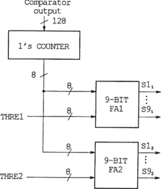
The integrator block takes the 128-bit comparator output and finds the number of matched and masked bits of the shift register. Its block diagram is shown in Fig.2.6. It contains a I ’s counter block, two 8-bit tristate unidirec tional buffers, an 8-bit adder, and a 9-bit 2-to-l multiplexer. The I ’s counter block is a combinational logic consisting of half-adders and full-adders in an inverse binary tree form. It simply counts the number of I ’s in the 128-bit comparator output. The tristate buffers at the output of I ’s counter has dif ferent purposes and different enable signals where the INT signal is produced by controller block and the M /S signal comes from the status register. The buffer having enable signal INT is used to read the 8-bit output of the I ’s counter through the data bus. That is, the microprocessor can read the I ’s counter output while doing correlation. This is an importcint property of the correlator because it provides an immediate result of the correlation to be able to make some decisions before continuing. Additionally, the output of I ’s counter gives more detailed information than the SYN pulse about the correlation. In other words, by looking at the I ’s counter output, one can calculate the number of matched and masked bits in the 128-bit shift regis ter and can learn the noise level on the incoming data. The other tristate buffer with enable signal M /S is used to send the I ’s counter output to the bidirectional pins CO to C7. This is necessary when two chips are cascaded to make a 256-bit correlation. In this case, the chip operating as slave must 'send its I ’s counter output to the one being master through 8-bit bus C0-C7. So, when M /S bit is low tristate buffer is enabled and I ’s counter output is seen at the output pins and when M /S bit is high tristate buffer is disabled emd its output is in high impedance state. The 8-bit adder in the integrator block is used to be able to make 256-bit correlation. It adds two I ’s counter block outputs in the master and slave chips resulting in a 9-bit number at the output. Then the output of 8-bit adder is multiplexed with the I ’s counter output by means of the 9-bit 2 to 1 multiplexer of which the select signal is M /S. The multiplexer output is the output of I ’s counter if M /S bit is high otherwise it is the output of 8-bit adder. Thus, by using this multiplexer, desired correlation score depending on the correlation length can be sent to decision maker. Consequently, the intermediate results of the correlation are prepared by the integrator to be used in decision maker or to be read by the microprocessor.
The decision maker is the block which gets the integrator output and the error tolerances kept in the threshold registers, TH REl and THRE2, and decides whether the sync word is detected or not. Therefore, it has two outputs which are SYN and INV. Its block diagram is shown in Fig. 2.7.
comparator output
To decision maker
Figure 2.6: Block diagram of the integrator.
Integrator output
THREl
THE^2
CLK CLR INV SYN
The decision block contains mainly two 9-bit adders, a 2 to 1 multiplexer, and two D-latch with a reset. The 9-bit adders are used to add the integrator output with the error tolerances. As shown in the figure, these adders have only the most significant two sum outputs that are the only ones needed to produce SYN and INV pulses. The two input “or” gate ensures that if INV signal is high, SYN signal is also high because, as mentioned earlier, when an inverted sync word is detected SYN and INV must be both high. Finally, the values of SYN and INV outputs are latched in every low-to-high transition of the CLK signal in two master-slave flip-flops. Thus, they can be read by the microprocessor using the status register. The master-slave flip-flops have the same clock signal with the shift register and so at the beginning of every clock cycle, as a new data enters into the shift register, the SYN and INV signals produced by using the previous data are latched into flip-flops. By means of the reset of flip-flops, the SYN and INV outputs can be reset while generating PRBS where these outputs are not needed.
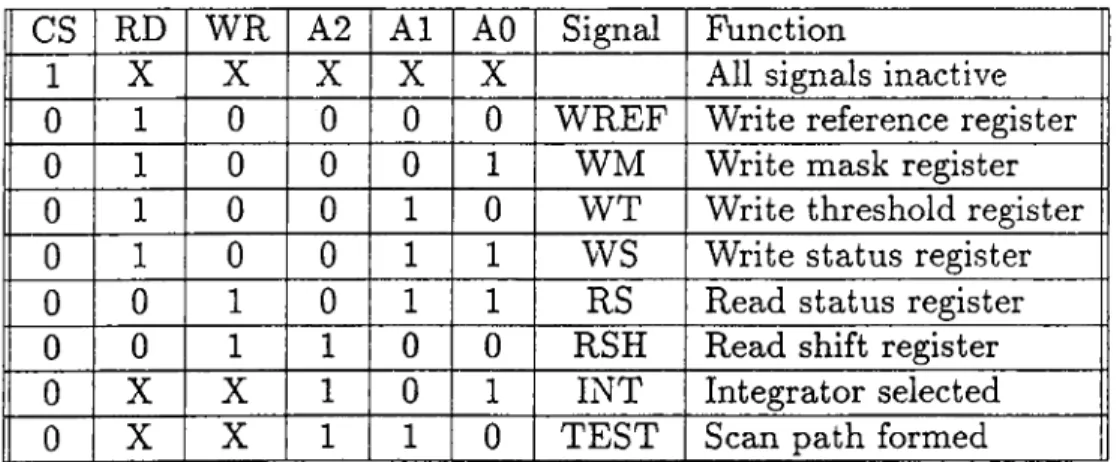
The controller block is used to produce timing signals for the registers and for the purpose of testing. Besides the test signal which is used in testing, it generates read and write signals for the registers by using the address signals (A0-A2), CS, RD, and W R signals. It decodes the address signals to select the registers or other blocks and produces eight different signals as shown in Table 2.2. Here the X values are used for don’t care conditions. While the CS is high, all output signals become inactive, i.e. low, irrespective of all other input signals to the controller.
CS RD W R A2 A1 AO Signal Function
1 X X X X X All signals inactive
0 1 0 0 0 0 W REF Write reference register
0 1 0 0 0 1 W M Write mask register
0 1 0 0 1 0 W T Write threshold register
0 1 0 0 1 1 WS Write status register
0 0 1 0 1 1 RS Read status register
0 0 1 1 0 0 RSH Read shift register
0 X X 1 0 1 INT Integrator selected
0 X X 1 1 0 TEST Scan path formed
Table 2.2: Function table of the controller block.
2.3.3
Pin Description
The correlator has 28 pins and its pin diagram is shown in Fig.2.8. Three of them are chip select (CS) input pin, read (RD) and write (W R) signal pins which are all active low and controlled by ¡j,F. The other ones are:
SER IA L DATA OUT COUNTER OUTPUT
INTERRUPT
Figure 2.8: Pin diagram of the correlator.
1. D0-D7: Bidirectional, tristate 8-bit data bus. When CS is high it is in high impedance state. Otherwise it is either in the write or read mode. 2. A0-A2: 3-bit address pins in order to select the internal registers and
integrator block and to produce a test signal in the chip.
3. CLK: It is the clock generated by digital phase-lock loop (DPLL) such that the incoming data can be taken into the 128-bit shift register. 4. SIN: Serial data input to the correlator. Data at this pin is latched to
the 128-bit shift register at the low-to-high transition of the CLK. 5. SOUT: Serial data output from the correlator. At the low-to-high tran
sition of the CLK, the least significant bit of the shift register is seen at this pin during a period of the CLK.
6. C0-C7: Bidirectional, 8-bit integrator input/output bus which is used to perform 256-bit correlation. That is, in cascade connection the 8-bit busses of two chips are connected to each other and the slave chip sends its I ’s counter output to the master chip through this 8-bit bus.
7. SYN: Sync output pin. When a sync word is detected it makes a tran sition from low to high and remains at high state for one CLK cycle.
2.4
Modes of Operation
As mentioned previously, the chip can function in two modes which are the correlation and PRBS generation modes. Selection of these modes is done as shown in Table 2.3. The operation mode of the chip is determined by the PRBS bit in the status register. In order to switch from one mode to another the state of this bit must be altered. Although the same circuitry is used in both modes, the chip performs totally different functions in two modes. In the following two subsections operation of the chip in two modes is presented in detail. PRBS M /S Operation mode 128-bit correlator(SLAVE)
0
256-bit correlator(MASTER) X PRBS generatorTable 2.3: Selecting modes of the correlator.
2.4.1
Correlator M ode
In order to operate the chip as a correlator, the PRBS bit in status register must be set to low. In addition to PRBS bit, also M /S bit in status register must be set to a value to determine the length of the correlation which is 128-bit or 256-bit. In this mode the chip perform the basic function:
N
CORRELATION
=OR{XNOR[Di,
R . · ) , M . )t = l
where the D{ are the current contents of the 128-bit shift register which holds the data, the R,· are the corresponding values in the reference register, and Mi are the corresponding latched masking values. The mask function, implemented with one OR gate per bit, tells the chip to include only a speci fied subset of 128-bit shift register bits in the final correlation score.
N
is the total number of shift register taps which is equal to 128 or 256 depending on the length of the correlation.In the correlator mode, after setting the PRBS bit in the status register to low, it is determined that whether a 128-bit or 256-bit correlation is to be done and then the M /S bit in the status register is set to low or high according to the correlation length. If a 128-bit correlation is done, this bit is set to low and we call such a chip as slave. On the other hand, if a 256-bit correlation is done, two chips are cascaded and one of them is called as master whereas the other one is called as slave. As opposed to slave, in the master chip, the M /S bit in status register is set to high and this means that the final 256-bit correlation result is to be produced by the master chip. The only difference between the functions of these two types of chips called master and slave, although they have the same hardware, is that one of them produces a 256-bit correlation score while the other produces a 128-bit correlation score. This is an important property of the correlator chip that by controlling a bit in the status register, the correlation length can be doubled. In other words, it is sufficient to change the state of M /S bit in order to determine the correlation length.
In 128-bit correlation, the reference register is loaded with the sync word and the mask register is loaded with the masking data in 16 write cycles of the /xP. The sync word is chosen by the user and it can be changed at any time only by loading the reference register with the new sync word. This can be done by putting the reference register address and the data on the 3-bit address bus and 8-bit data bus for 16 write cycles of the /xP. The mask register content determines the subset of the 128-bit data in the shift register to be included in the correlation. That is, the “ 1” s in the mask register means that the corresponding bits in the shift register are considered as “don’t care” . This is also an important property of the correlator chip because by having this feature the chip can detect the distributed sync words which may have data bits among the sync bits. This means that, if it is desired, sync words of length less than 128 can also be detected. These capabilities makes the correlator flexible about the sync word length and the distribution of its bits. Now, after the reference and mask registers are loaded, there comes the loading of the threshold register consisting of two 8-bit registers, THREl and THRE2. THREl is related with the noninverted sync detection and THRE2 is related with the inverted sync detection. TH REl register must be loaded by the maximum number of errors that can be tolerated and cis it is clearly understood, this register content can have values between 0 and 128. THRE2 must be loaded by 255 (all I ’s) minus (maximum number of tolerable errors + number of I ’s in the mask register). This is equal to the I ’s complement of the binary number which is equal to the tolerable errors plus number of
masked bits. Here, this number in the register THRE2 is to be used for subtracting the number of error tolerance from the number of erroneous bits in the shift register. If the result of the subtraction becomes positive, this means that the number of erroneous bits is greater than the number of error tolerance. But if the result of the subtraction is negative then the number of erroneous bits is smaller than the number of error tolerance. Consequently, an inverted sync word is detected when this subtraction results in a negative number. Actually, by using this method, a Hamming distance between input data and reference data is calculated and if this Hamming distance is below a given threshold, it is decided that a sync word is detected.
Now, the correlation can begin with the first bit of the incoming data entering to the 128-bit shift register from serial input, SIN. Data is latched to the first master-slave flip-flop of the shift register at the high level of the clock. Since master-slave flip-flops are used in the shift register, the new content of it for calculating the correlation score becomes available after high-to-low transition of the clock. After 128 clock cycles the first bit of the incoming data appears at the serial output SOUT and if a sync word is detected, SYN and/or INV outputs become high at the 129’th pulse as shown in Fig. 2.9. As it is clear, correlation is done for every clock period and calculations start after the falling edge of the clock and finish before the next rising edge of the clock. Thus, all calculations must be done while the clock is low and it must be decided whether the sync word is detected or not before the rising edge of the clock. Therefore, the duration between the falling edge of the clock and the time at which the decision maker output becomes stable determines the speed of the correlator and frequency of the clock.
SI _r
8 SO first pulse CLK SYNC ^ ^1 2 8‘'th pulseJlJl_rLn-TLrL
SYM INV I 1— -J I I - I ________L I Figure 2.9: Timing diagram of the sync detection.When the outputs of the shift register become valid, meaning that the comparator inputs axe ready, comparator block checks whether the shift and reference register bits are the same or not and also looks for the mask register bits in order to understand which shift register bits are to be masked (i.e.
don’t care). Then it produces a “ 1” at the output for the matched or masked shift register bits and produces “0” for others. The comparator block has a 128-bit output which is connected directly to input of the I ’s counter in the integrator block. I ’s counter finds the number of comparator output bits which are “ 1” and produces an 8-bit number having a value between 0 and 128. In 128-bit correlation this is the output of the integrator block which is fed into the decision maker. In decision block, this 8-bit number is summed with both threshold register outputs, TH REl and THRE2. This configuration is shown in Fig. 2.10. In this way, the I ’s counter output is summed with the error tolerances held in the threshold register.
Comparator output
Figure 2.10: 128-bit correlation scheme.
We are interested only in the most significant output bits of the 9-bit adders in order to decide about the detection of a sync or inverted sync word as shown in Table 2.4. The output of that 9-bit adder which adds the I ’s counter output with the output of TH REl can have values between 0 and 256. If the output of this adder is between 128 and 256, this means that the number of matched and masked bits plus the tolerable erroneous bits in the shift register is greater than or equal to 128. In other words, if the 8’th bit of the 9-bit adder output is 1, it means that a sync word is detected. For deciding about the inverted sync word detection, other 9-bit adder which adds the I ’s counter output with the output of THRE2 is used. If the most significant bit is “ 1” meaning that the output of the adder is greater than 255, there is
most significant bit is “0” , this shows that an inverted sync word is detected. So, when a sufficient number of bits come inverted with respect to bits in the reference register, an inverted sync word is detected. Actually, in the case of inverted sync word detection, both the sync (SYN) and inverted sync (INV) outputs of the decision maker becomes high. In 256-bit correlation.
S8i 502 SYN INV
0 1 0 0
1 1 1 0
0 0 1 1
Table 2.4: Decision table for the sync detection.
two 128-bit correlator chips are cascaded as shown in the Fig. 2.11. The reference, mask, and threshold registers in both chips are similarly loaded as in the 128-bit correlation. But this time, the contents of TH REl registers can have values between 0 and 255 which cbrresponds to the maximum number of error tolerance. In the same way, the THRE2 registers are loaded with the I ’s complement of the binary number which is equal to the number of tolerable errors plus the number of masked bits.
SERIAL DATA IN CLOCK SERIAL DATA OUT CHIPSELECTl CHIPSELECT2 WRITE READ DATA BUS ADDRESS B U S ■ S I N CLK s o u r S I N CLK s o u r
BAC128
8BAC128
INTERRUPT ---- S Y N ( M A S T E R ) C 0 - C 7 - 7 ^ C 0 - C 7 (SLA V E) C S W R R D D 0 - D 7 A 0 - A 2 C S W R R D D 0 - D 7 AO--A2Figure 2.11: 256-bit correlator.
We call the first chip as master since it calculates the final correlation score and produces a sync pulse if a 256-bit sync word is detected. The incoming data first enters to the serial input of the master and after 128 clock cycles
it is seen at the output of this chip. Then the data enters into the slave from its serial input and at the end of the 256’th clock cycle it appears at the serial output of this chip. At the falling edge of the 256’th clock pulse, the comparison between input data and reference data is started in the chips and both chips produce their intermediate results which correspond to 12S- bit correlation score of each chip. Later, the slave sends its result to the master through the 8-bit bus CO — C7. Then the master sums the result coming from the slave and its result and sends the summation output to the decision maker block as shown in Fig. 2.12. As in the 128-bit correlation, additions with the TH REl and THRE2 outputs are performed by using two 9-bit adders. The decision for the 256-bit sync or inverted sync detection is made as shown in Table 2.5. It is clear that, this decision is made only in the master chip so the SYN output of only this chip is connected to the interrupt pin of the microprocessor. In fact, also the slave chip makes some calculations and decisions and it may produce a sync pulse too. However, its SYN output pin is not connected to anywhere and therefore its decision is not taken into consideration in the 256-bit correlation.
S ’O i 5 9 2 S Y N I N V
0 1 0 0
1 1 1 0
0 0 1 1
Table 2.5: Decision table for 256-bit sync detection.
2.4.2
P R B S Generator M ode
The configuration for operating the chip as PRBS generator is shown in the Fig. 2.13. In fact, this scheme realizes a linear feedback shift register used in PRBS generation. Here the 128-bit shift register is loaded with an initial state chosen by the user and at every clock cycle its contents changes randomly. The mask register is used to select the necessary taps from the shift register outputs. In order to do this, the mask register bits corresponding to the selected taps are loaded with zero and all other bits are loaded with one.
SIN
Figure 2.13: The configuration for PRBS generator.
Thus selected taps of the shift register appear at the corresponding com parator output bits while other comparator outputs are 1. Then the I ’s counter in the integrator block counts the number of I ’s at the comparator outputs. The I ’s counter behaves as a huge EX-OR gate with 128 inputs because we are interested in only the least significant bit (LSB) of its output. That is, if there is an even number of I ’s at the comparator output, LSB will
be 0 but if there is an odd number of I ’s then LSB will be 1. In this way, the selected taps in the shift register would be EX-O R’ed and LSB representing the E X -O R output is fed back to the serial input of the shift register by using a multiplexer which is controlled by PRBS status bit. Consequently, a new pseudo-random bit enters to the shift register at every clock cycle and at the same time this bit can also be seen at SOUT. In other words, PRBS generator output is taken from SOUT because we don’t have to wait for a random bit propagating from serial input through shift register to the serial output.
In this mode, the generated bit sequence will have a nearly random dis tribution if the tap points are suitably chosen, because the length of the shift register is quite large. The sequence repeats itself after a large number of clock cycles. But here the important thing is the initial state of the shift register. If the initial state is known, the state that the shift register will have after a certain number of clock cycles can be predicted. Due to these properties of PRBS, it can be used for sync word generation, i.e. a portion of this sequence can be chosen as a sync word.